Power Stamp Alliance Exposes Ice Lake Xeon Details: LGA4189 and 8-Channel Memory
by Ian Cutress on April 9, 2018 11:42 AM EST
For everyone waiting for Cascade Lake, Intel’s next server Xeon platform, to be launched, noise is being made from the Power Stamp Alliance and its members about the platform beyond Cascade Lake. Alliance member Bel Power Solutions, along with the Power Stamp website, have exposed several details on the Ice Lake Xeon platform.
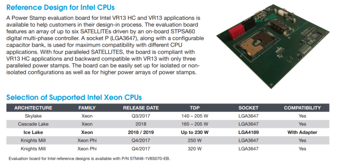
The first element of the information is the new socket, set at LGA4189. This is compared to the current Xeon socket, standing at LGA3647, which currently supports the Skylake Xeon family as well as the upcoming Cascade Lake Xeon family. According to the documents, the power pin implementation between the new LGA4189 and LGA3647 sockets are compatible via an adaptor: this isn’t to say the CPUs themselves will be, but it would appear that all the Skylake/Cascade Lake/Ice Lake Xeon families will have a similar power implementation. The reason why we mention the power implementation only is because the Power Stamp Alliance (and Bel Power Solutions) is only dealing with DC-to-DC converters for the platforms, driving efficiency from a high 48V input correlating with the Open Compute Project (OCP) standards and deployments.
Also in this image (and verified at Power Stamp) are the power ranges for Cascade Lake (165-205W, similar to Skylake Xeons) and for Ice Lake (set to go to 230W). Should the new Ice Lake Xeon platform incorporate features such as OmniPath or on-package FPGAs, which Intel has teased future Xeon platforms to be, then 230W is well within the reasons of possibility. Also, having a high DC-to-DC efficiency is going to assist with overall power consumption and power loss.
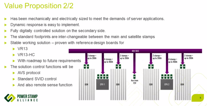
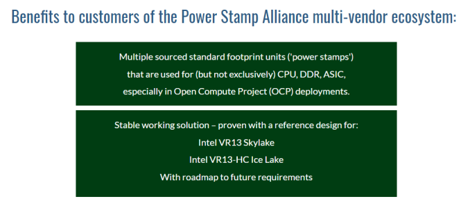
Delving into the documents, the Power Stamp Alliance designates two code names in play: VR13 (for Skylake and Cascade Lake) and VR13-HC (for Ice Lake). The HC in this case stands for high-current, and the documentation shows ‘a typical’ VR13-HC implementation with two CPUs and sixteen DDR4 memory slots for each CPU. The Bel Power systems documents goes on to say that a VR13-HC system (Ice Lake) with four power stamps meets the VR13-HC minimum requirements, while only three are needed for VR13 (Skylake/Cascade).
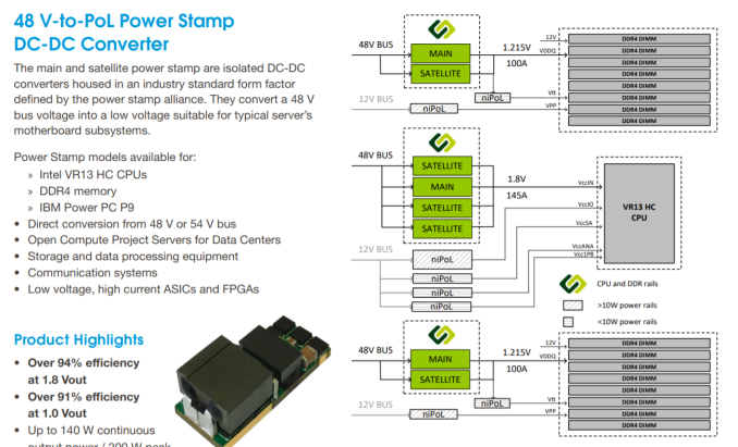
The images shown above and below point to Ice Lake Xeons being equipped with native eight-channel DDR4, given how Intel dropped 3 DIMM per channel support with Skylake. This comes through the chip directly, rather than implementing memory buffers, such as the Jordan Creek implementation on the E7 v4 family. With the 8-channel design, one might assume Intel boosting the maximum memory capacity of the base Xeon processors from 768GB to 1TB, although we should wait to see if that is going to be the case. If Intel is using the same on-chip network implementation as Skylake, it would also mean that one of the segments that previously used for a tri-memory channel controller actually has enough space for a quad-memory channel controller.
No special mention is made regarding XPoint memory support. Parts of the documents state that a set of 8 DRAM slots and two power stamps should be good for 100-200A at 1.215 V for VDDQ, implying that a set of 8 memory sticks should be able to draw around 120W-240W, or ~15-30W each. Varying numbers have been postulated as to the power draw of XPoint modules, but most numbers are within this range.
More information from the Power Stamp Alliance is set to be given at the Open Compute Summit, happening in late May. The Alliance consists of STMicroelectronics, Artesyn Embedded Technologies, Bel Power Solutions, and Flex
Sources: Bel Power Solutions, Power Stamp Alliance, via Twitter
*This article first stated that the OCP Summit was going to happen in Late May. It actually happened in Late March already.


37 Comments
View All Comments
Khenglish - Monday, April 9, 2018 - link
I can't shake the feeling that using a 48V bus is a mistake. Nearly all power FETs built today have a 30V Vds max. Using 48V means all new power FETs need to be designed.24V would have been more reasonable. Major efficiency improvements over 12V while not requiring new hardware to be designed.
LarsAlereon - Monday, April 9, 2018 - link
The thing is there's already a 48V DC supply available in the data center, so running it's worth designing new hardware to avoid a conversion stage.The_Assimilator - Monday, April 9, 2018 - link
It is way, way, WAY past time for the ATX standard to move to 24V.edzieba - Tuesday, April 10, 2018 - link
Moving to 48V would be even better: it would effective mean quadrupling any existing trace design's power carrying capacity. As an example, the 75W PCIe bus power would jump to 300W without needing new hardware designs, allowing pretty much every GPU on the market to switch to bus power only, eliminating a whole pile of internal wiring (reduce both material cost and assembly cost).Samus - Tuesday, April 10, 2018 - link
Isn't PowerPC (Power9) already 48v?CPU Power "Stamps" have been an IBM trademark since PowerPC G3's where the FET's, voltage conversion (and external cache - a norm at the time...) were on the same PCB. This greatly simplified motherboard architecture and allowed for some pretty ridiculous life cycles.
The PowerMac's are a great example of this. Board that shipped with 300MHz processors could be upgraded a DECADE later to the latest G4 architecture running dual 1.8GHz CPU's - using THE SAME motherboard. It was no surprise these systems held their value for 10-12 years until the G5 architecture was discontinued and no further upgrade path was possible.
flgt - Monday, April 9, 2018 - link
That doesn’t sound right. There are plenty of high voltage FETs available. There are trades to be made in other FET parameters when you go high voltage though that can degrade efficiency in that stage. There is hope that GaN can overcome a lot of those drawbacks. They’re going to have to get the voltages up in these DC systems so the resistive losses don’t get out of control.[email protected] - Tuesday, April 10, 2018 - link
They are beating an ancient dead horse with this power solution utilizing Buck Converter Topology with PEAK efficiencies of 91%, which means efficiency as low as 82 - 85% at lower power levels. With 600W to memory and CPU that is 90W of heat. The new approach using GaN at 2MHz switching comes with a hope and prayer elevated frequencies will suffice. 48V to 1V reduction means a 2% duty cycle and probably 12 to 16 Buck converter phases. This is a ludicrous solution because 2% duty cycle at 2MHz means ON periods of 10ns - oscillator jitter at that level is problematic. But worse than this the ferrite core's at 2MHz operate at 5 mT flux density at best, which means higher frequency will not result in reduced ferrite core size. It is time to stop beating this dead horse topology and switch to modern topologies using hybrid PWM-resonant switching, as the Cuk patents from 8 to 10 years ago demonstrated with >98.5 to 99% efficiency. To wit: reduce heat by over 90% and use just one or two phases. A big advantage of fractional resonance and resonance scaling is the ferrite core is eliminated entirely even at 50kHz switching, which reduces power supply footprint by 85%. Chip manufacturers like this dead horse as they sell lots more chips. It is frustrating to watch power electronics engineers engage in this ludicrous power solution, because they believe the marketing hype of the power chip manufacturers. There is a disaster in the making here.[email protected] - Tuesday, April 10, 2018 - link
For those interested in the refinements of power electronics and the topology issues mentioned above, here is a link to the commentary at the recent Rap Session 1 at APEC 2018. I am just not impressed by Intel's new servers, and Intel's engineers should know better. But apparently they do not. Certainly the acumen of organizers of the recent APEC 2018 conference leaves a lot to be desired, where profit rules over common sense.https://www.linkedin.com/pulse/biggest-impact-devi...
iter - Tuesday, April 10, 2018 - link
When it comes to maximum profits, intel bets on other horses rather than engineering excellency.[email protected] - Tuesday, April 10, 2018 - link
The real problem is consumers pay for a huge number of ferrite cores, MOSFET power stages and controllers, when a much smaller footprint at a small fraction of the cost would increase both manufacturer's profitability, as well as eliminating substantial heat for a significant reduction in motherboard cost. Lackadaisical engineering prowess places the cost at the consumer big time. Imagine 12 phase Buck VRMs with 12 ferrite cores are reduced to zero, where inductors with resonance scaling are reduced to 10nH as 5mm copper traces on the motherboard. That is a very big deal in cost and effort, with ceramic capacitors eliminating the larger capacitors. Intel does not bet per se, they are just victims of really bad practices, and Intel is not alone in this.This issue is compounded with ATX PSU, GPU VRMs, and motherboard VRMs connected in series. The ATX PSU is 80% efficient in supplying power, then various VRM's convert that output power with another 80% conversion efficiency on top of that, so in the end almost 60% of input power goes into waste heat due to cascaded DC-DC conversions. A near 40% waste heat could be reduced to 5%, the ATX power supply could be 20% of its current volume, and individual VRM footprints <10% of their current sizes (without ferrite chokes). Looked at in those terms we are paying a lot of money for no gain. Power electronics manufacturers are very happy their hype is working in their favor. We just keep losing money in our purchases. Using single cycle settling times with modern topologies also eliminates the complexity of the power controllers, which could be integrated into a single chip with the power stage. A Ryzen like takeover is needed in the realm of motherboard power supplies. I hope AMD is listening. AMD! Please tell me you are listening. As a retired member of the electronics industry, I can say I am most disappointed in where this industry currently stands. OK! I will rest from my rant now, and hope for change.