Original Link: https://www.anandtech.com/show/5089/sandy-bridgee-and-x79-the-asus-p9x79-pro-review
Sandy Bridge-E and X79 – The ASUS P9X79 PRO Review
by Ian Cutress on November 14, 2011 3:01 AM EST- Posted in
- Motherboards
- Asus
- X79
It seems that every few months or so, we get a new socket and a slew of new chipsets from Intel. If we go back as far as 775 (mainstream), in consumer land, we have covered 1366 (enthusiast), 1156 (mainstream) and 1155 (mainstream). This is in contrast to AMD’s backwards compatibility progression of AM2/AM2+ to AM3/AM3+ (if you ignore Llano and Fusion).
Information has been flying around about the new X79 enthusiast platform for some months now, especially when looking for a replacement for X58. Needless to say, X79 aims at high end and high price. There are the main changes that everyone knows and cares about – quad channel memory and 40 PCIe lanes strike high on anyone’s list about X79. Does that mean the chipset is really for those who want >16 GB of memory, or 2/3 way GPU action?
 Block Diagram.png)
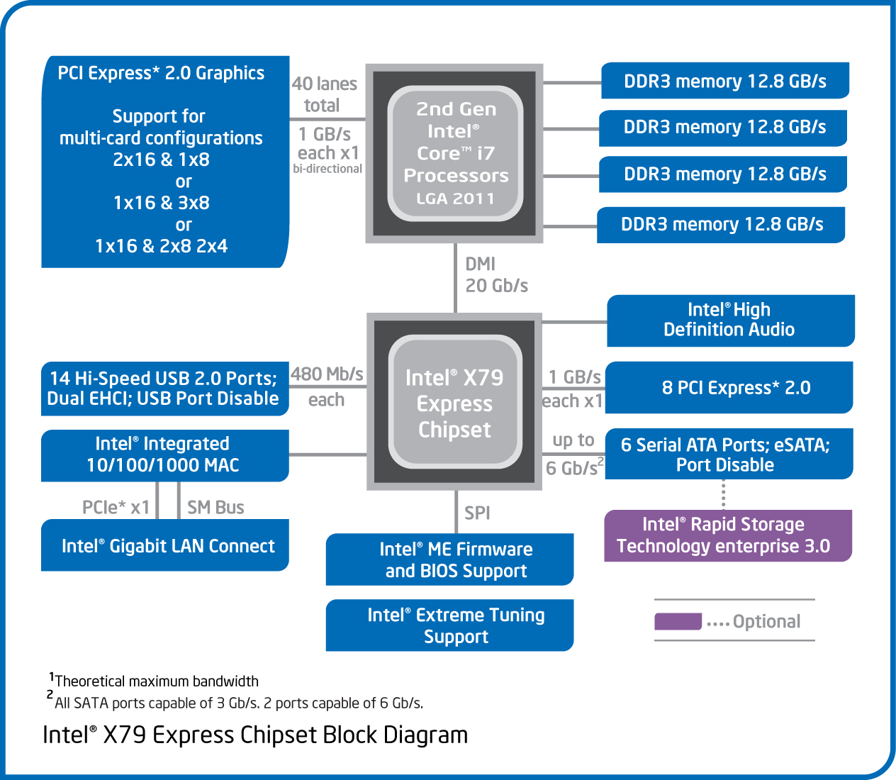
Above is a block diagram of the routing of the LGA 2011 socket and the X79 Platform Controller Hub (PCH), taken from Intel’s DX79SI motherboard information, which will be reviewed in due course. A few points are specific to that board (dual LAN controllers, USB 3.0 implementation), but it covers the basics of most X79. As we can see, the GPU PCIe lanes are split through multiplexers and switches for x16/x8 or even x4 speeds, depending on the motherboard in question. The connection via DMI from the CPU to the PCH gives the motherboard most of the functionality – PCIe x1, SATA, Legacy IO, TPM, USB 2.0, Audio, Ethernet etc. Most of these features are obviously adjustable by the motherboard manufacturer, in terms of quantity (decrease or increase through controllers), or manipulation, for example ASUS’ SSD Caching, as explained in the ASUS review later.
Firstly, let us look at which niches X79 and LGA 2011 are attempting to cover.
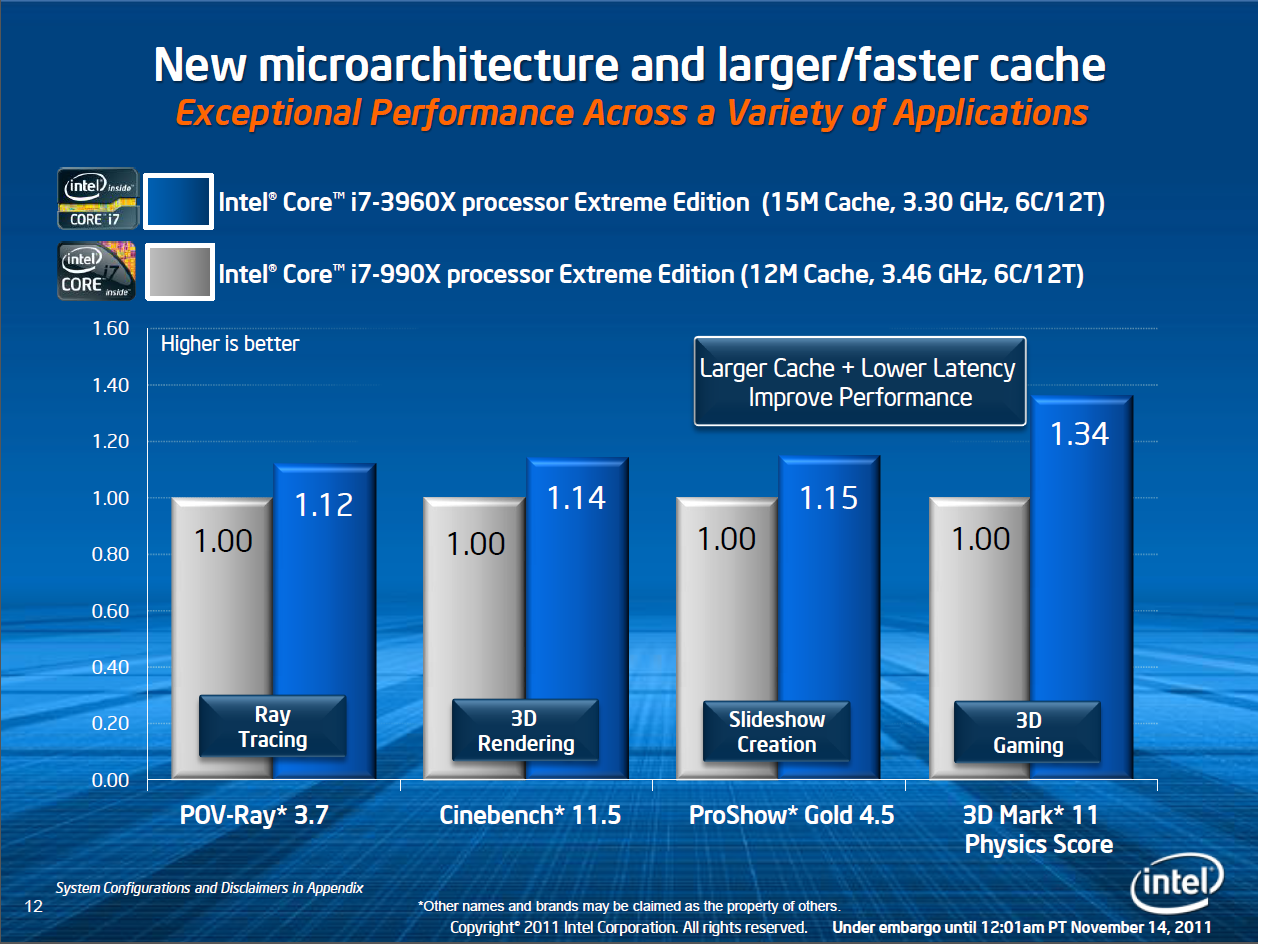
On Anand’s article regarding the CPUs, it is clear to say that anyone wanting performance can find it in Sandy Bridge-E. If you are willing to pay top dollar, you get a top CPU with six cores/twelve threads that will run between 3.6 GHz and 3.9 GHz (depending on CPU load) in a 130 W envelope. With a little push, this could easily see 4.5 to 4.7 GHz while on the Intel branded water cooler being sold separately. While this will not make much of a difference for gamers, we can see the allure for any CPU intensive tasks that are not already GPU accelerated – video encoding or rendering being obvious view points. The following is a slide from Intel’s press kit, comparing the performance of SNB-E i7-3960X to the i7-990X, where the main differences to X58 are the microarchitecture improvements (Nehalem->Sandy Bridge), the memory, and the larger cache:
Memory is a big part of X79, as we are introduced to quad channel memory on a mainstream consumer level chipset, compared to the previous enthusiast chipset, X58, where the push was in tri-channel memory. Most X79 boards will cater for 8 DIMM slots (2 DIMMs per channel), though some will scale this back to 4 DIMM slots to save money and space on the board. Theoretically, a 4x2 configuration will cater up to 64 GB of memory when using 8 GB memory sticks, though users will perhaps be looking in the $1600 range for such a kit (for example, Corsair’s Dominator 4x8 GB DDR3-1866 C9 kit CMT32GX3M4X1866C9) which surpasses the cost of a motherboard+CPU in one swoop. By specification, population of 8 DIMMs should make a motherboard default to 1333 C9 speeds, while when only using 4 DIMMs should give 1600 C9.
There are issues to the memory that a lot of people will consider – does anyone ever need 64 GB of memory? Even if it were populated with relatively cheaper 4 GB sticks, does anyone ever need 32 GB of memory? For the most part, no, however there is always a need for Virtual Machine memory, computational scientists requiring large data sets under a tighter budget, or animators requiring large rendering memory budgets. The flipside of the memory is that most motherboard manufacturers will support high memory frequencies – for example, as shown in the P9X79 PRO, up to DDR3 2666 MHz is selectable on the divider alone. In some pretesting, using a G.Skill RipjawsZ 4x4 GB kit, I have been able to hit 55 GB/s memory bandwidth quite happily. However, as stated previously, there are few users that this will be aimed at, but that is kind of the purpose of such a chipset.
There is argument here that Intel could have used dual channel memory for the high end – it would have reduced the pin count on the CPU (perhaps put it into an 1155 envelope, disregarding the PCIe connections) and ultimately the cost of the platform. Memory bandwidth is not a struggling feature for a lot of users, but those who found the memory bandwidth of X58 the limiting factor will enjoy the quad-channel of X79. Despite this, the specification does allow single, dual and tri-channel operation for X79, so it is completely possible that if micro-ATX or even mini-ITX motherboards are produced, they may scale back to two DIMM slots for dual channel operation. This gives a consumer up to 16 GB of memory, but should provide the same performance in non-memory bandwidth limited scenarios to Sandy Bridge based applications.
For the gamers and GPU users, we finally get full x16/x16 native compatibility in the PCIe world, without the need for any performance reducing NF200 solutions. X79 for the most part will see motherboards spouting x16/x16, x16/x16/x8, x16/x8/x8/x8, x8/x8/x8/x8 or even x16/x8/x8/x4/x4 variations depending on the PCIe layout of the board, the size of the board, and the manufacturer. For all intents and purposes, in gaming, we are not expecting this to make any difference for the first two GPUs. Very few gamers will be using more than two, and again, this chipset is aimed at ‘no price too much’ style scenarios. Where it will probably be handier is in the land of GPGPU, where CPU to GPU bandwidth may have been the major limitation in running simulations.
We cannot get away from the fact that for a lot of X79 motherboards, the PCIe GPU lanes will be post-specified at PCIe Gen 3. The chipset, and the motherboards in X79, should all display Gen 3 compatibility for the GPU slots (usually for the PCIe x8/x16), but this currently means relatively little for consumers until Gen 3 products are released to the market. There is also the fact that it cannot be properly tested in a real-world context until then – depending on how exactly the GPU manufacturers utilize the new technology. As a result, the initial batches of X79 motherboards may require a BIOS update to activate this functionality. I was lucky enough to observe an ASUS Z68 Gen 3 board running an Ivy Bridge processor at a recent invitational event, where ASUS were clearly stating that all their PCIe Gen 3 products are correctly implemented.
It is worth having a look at PCIe Gen 3, if only for a couple minutes. Inside the Intel Chipset implementation, it states:
Intel Core i7 and Intel Xeon processors in an LGA2011 package support PCI Express add-in graphics cards via the board’s PCI Express x16 connectors. These processors support the following generations of PCI Express:
- PCI Express 3.0 with a raw bit rate of 8.0 GT/s results in an effective bandwidth of 8.0 Gb/s each direction per lane. The maximum theoretical bandwidth of the x16 interface is 16 GB/s in each direction, simultaneously, for a bandwidth of 32 GB/s.
- PCI Express 2.x with a raw bit rate of 5.0 GT/s results in an effective bandwidth of 4.0 Gb/s each direction per lane. The maximum theoretical bandwidth of the x16 interface is 8 GB/s in each direction, simultaneously, for a bandwidth of 16 GB/s.
I want to draw attention to 3.0 and 2.x, and the comparison between GT/s (GigaTransfers per second) and bandwidth. It states, for 3.0, that there is a raw bit rate of 8.0 GT/s, and an effective up/down bandwidth total of 32 GB/s. For 2.x, there is a raw bit rate of 5.0 GT/s, and an effective up/down bandwidth total of 16 GB/s. This means there is a distinctive change in how PCIe 3.0 and 2.x operates – PCIe 2.0 uses an 8b/10b encoding scheme, which causes a 20% overhead; whereas PCIe 3.0 uses a ‘scrambling’ technology using binary polynomials and a 128b/130b encoding scheme, reducing overhead to 1.5%. So whereas PCIe 2.0 was a natural progression to PCIe 1.x, this is where the new 3.0 specific features are required in terms of processor and chipset.
The landscape of overclocking has also changed… slightly. The land of X58 overclocking was as varied as one could get – full multiplier and BCLK adjustable to get the balance a user wanted. Sandy Bridge and P67/Z68 changed all that, due to the internal clock generator, effectively being multiplier only. While this made overclocking easy for users and system builders alike, there were some outcries from various overclocking communities about ‘taking the fun’ out of overclocking. Sandy Bridge-E attempts to bridge the two systems with an overclocking hybrid of sorts. It all comes down to clock generators.
The initial CK505 clock generator, at 100 MHz, is split several ways – one to the CPU/memory, one to the PCIe, and one to the I/O. These splits act to gear the clock generator, allowing the user to adjust one without affecting the others. This opens up the CPU overclocking to a wider range of adjustments, rather than the 1-5 MHz sported on most Sandy Bridge/Cougar Point CPU and chipset combinations. A deeper look into how to overclock the Sandy Bridge-E platform is described later as part of the ASUS P9X79 Pro review. However, the broadside of SNB-E is that due to the design and the increased core count, it is expected that SNB-E processors may not overclock as well as Sandy Bridge for 24/7 use, leaving single core performance firmly in the hands of the mainstream processor market.
We are not afraid of overclocking 130W CPUs, despite the increased power draw and heat – a big feature of X58 was overclocking. However, while these SNB-E chips are also 130W, Intel is pushing the release of an Intel branded, all-in-one liquid cooler:
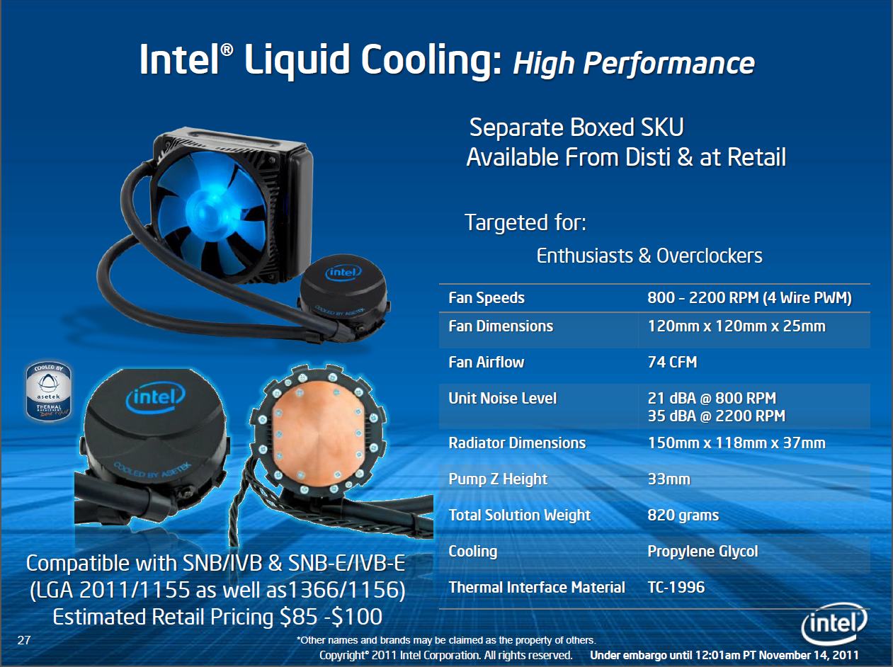
Made by Asetek, this is a simple 120mm single radiator cooler using propylene glycol whereby the fan plugs into a cable from the cooler, and the cooler plugs into the CPU fan header on the motherboard. This indicates that the pump and fan are both controlled by the onboard BIOS fan control implementation. In normal operation, using this cooler, I saw 61ºC in a forced 100% CPU load scenario (ambient 20ºC max) – in an overclocked (~30%) situation, this rose to 89ºC, where both liquid pipes to and from the cooler were warm. It’s not the most perfect water cooler on my brief analysis, but some substantial cooling will be required if users want an overclocked system. It also makes me wonder how Intel’s air cooler will fare, given that they suggest it is for stock systems only:

Lastly, we do lose a few features that have been on previous chipsets, or that were expected to be on X79. The most disappointing is perhaps the lack of USB 3.0 native to the chipset. It looks like we will have to wait until Ivy Bridge or even Haswell for updates on that end. Also, probably more of a carry over from P67/Z68, is that we still have a SATA 3 Gbps/SATA 6 Gbps discrepancy from the PCH. If AMD can stick 6 SATA 6 Gbps from their FCH implementations, it cannot be too much to ask for Intel to do it. It seems surprising then that we do not have Z68’s Smart Response Technology (SSD Caching) on X79 – though ASUS have devised a solution using a hardware/software combination which I will discuss later. Then there is the talk over SAS ports and compatibility – back at Computex when pre-release models of X79 boards were on show, they all had 6 SATA and 6 SAS ports on their models. But this was pulled from the specifications by Intel, for a variety of reasons. So while SNB-E and X79 are meant to be the pinnacle of performance and functionality, there is obviously still room for improvement if we literally want to have everything (no expense spared) in a chipset.
So, without further delay, let us rock on with one of the most important X79 motherboard releases – the ASUS P9X79 Pro!
In the pursuit of sheer performance, a user should aim to combine the ultimate CPU with the ultimate everything else – motherboard, memory, and so on. The latest enthusiast platform to hit our streets is Intel’s latest Sandy Bridge-E and X79 chipset, released today.
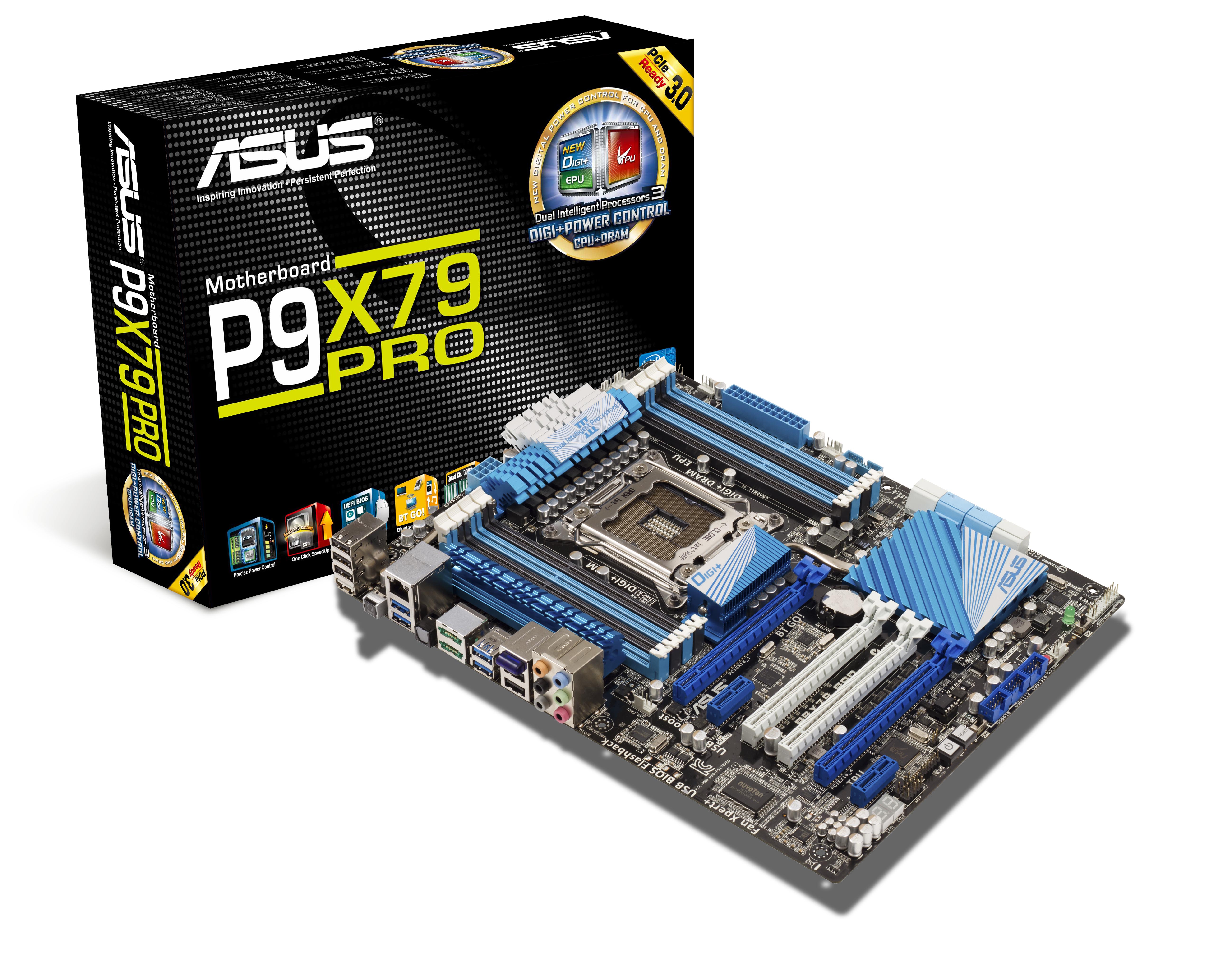
So to start a series of X79 reviews, we are going to have a look at what the X79 chipset brings to the table over other Intel chipsets, and the first motherboard under our microscope is the ASUS P9X79 Pro, coming in at an RRP of $329.99. Needless to say, this is fairly expensive in the land of motherboards, even when pairing it with a $1000 CPU. However, if previous Intel chipsets are anything to go by, ASUS Pro boards get a lot of attention. So the question becomes ‘Is it worth it?’
Overview
ASUS are impressive – as an innovator and as a product producer. Any company can stick an Intel chipset together on a board and sell as-is. It takes a large amount of highly skilled, consumer and technically oriented people to produce top level products, and ASUS have succeeded with aplomb on what seems to be their entire range.
One of the major plus points for the ASUS boards, including the Pro, is the implementation on X79 style SSD Caching. By a hardware/software combination, users can implement SSD caching via a specific pair of SATA 6 Gbps ports on the board. There is also ASUS USB 3.0 boost, which overcomes Windows’ USB protocol limitations to improve USB 3.0 speed. As expected on such an enthusiast board, an Intel NIC is used for improved performance and lower CPU usage.
The ASUS boards also include a feature called BIOS Flashback. This allows a user to write a new BIOS to the board via a USB stick without the need for CPU or DRAM being installed. In my opinion, this is a great idea, especially if the board shipping BIOS does not support a future processor being released.
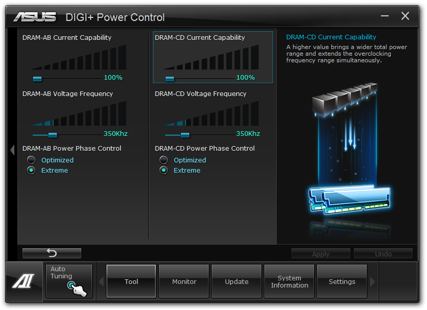
Power delivery is completely digital in the form of DIGI+, and adjustable to both the CPU and now the memory. On the Pro, six fan headers are provided onboard with high quality fan adjustment (both BIOS and software) thanks to their more expensive fan controller solution. The graphical BIOS is the typical ASUS fare we are used to, and I was impressed by the automatic overclocking functions which perform well, giving significant boosts in performance.
Points requiring a little adjustment on the Pro, at least from my point of view, start with the PCIe layout. While having three spaces between the main PCIe slots does wonders for GPU cooling, a lot of GPU manufacturers only put triple slot length connectors on board for SLI/CrossfireX, not quad length. This may cause extra expense for the consumers if their particular model did not come with the right cable, which surprises me when ASUS include SLI cables with the Pro, but not CrossfireX (ed: AMD has suppliers to bundle cables with cards instead of boards). Perhaps also expected is dual Gigabit Ethernet on such a board, given that there is plenty of I/O panel space. Even if this was a simple Realtek solution, if software was provided to enable Teaming, there would be users who would love the option. Lastly, I would have liked a USB 3.0 front panel addition in the box. All that said, ASUS states the Pro has an RRP of $329.99 and a standard 3 year warranty.
Visual Inspection
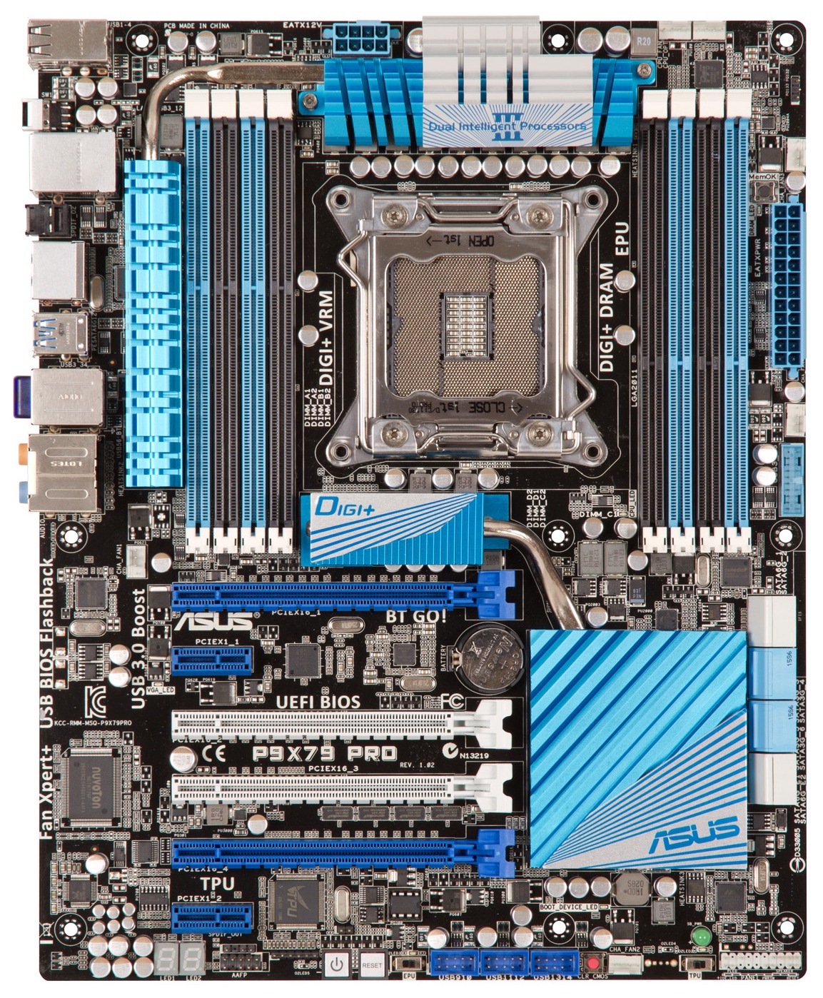
If you have never read any of AnandTech’s pre-X79 coverage articles before, the thing that will strike you most on any of these motherboards is the size of the socket. While the CPU die is only 20.8 mm x 20.9 mm, it supposedly requires 90lbs per square inch of pressure, up from 70lbs per square inch on previous platforms. As a result, we have a new CPU bracket holding the socket together, which uses two latches rather than one to hold the CPU in place. The mounting holes themselves are of similar ilk to Intel’s recent platforms in terms of spacing; however the screw size is reduced from previous platforms. Due to the extra pressure requirement, Intel are moving away from push-pin type coolers, and are aiming more at those that screw into the bracket directly. This means a move away from backplate type arrangements, and a step towards screw-ins. This is evident on the Intel all-in-one liquid cooler, which requires manual adjustment of the screws into the bracket, then tightening with a screwdriver.
The mass of DIMM slots is also of note, as this takes an obscene amount of PCB space either side of the socket. As mentioned before, there could perhaps be a call for motherboards with 2 DIMMs in a dual channel mode, in order to free up this real estate. Nevertheless, ASUS handily color codes the DIMM slots, where the blue ones should be filled first, then the black, for optimum performance. All these DIMM slots get in the way of the power delivery of course, and the Pro uses an 8-phase digital VRM for CPU power delivery. The relatively small heatsink above the CPU has a large surface area, and is connected via a heatpipe to another heatsink to the left of the DIMMs.
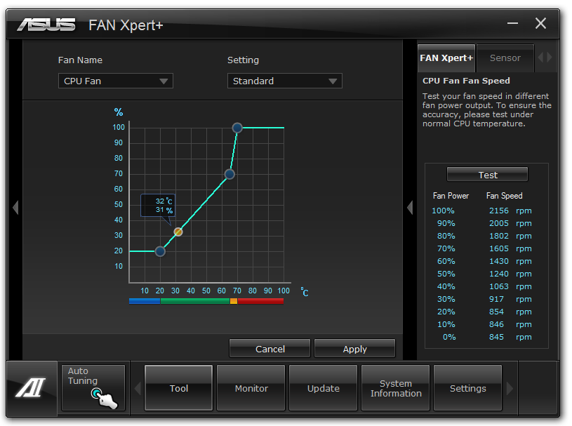
I like a board with a lot of fan headers – and ASUS have put six on this board, all under the control of their Q-Fan/Fan Xpert technology. These fan headers are located such that two 4-pin CPU headers above the right hand side DIMMs, one 4-pin chassis header beside the IO panel, two 4-pin chassis headers beside the 24-pin ATX power supply, and a final 4-pin chassis header on the bottom of the board. All of the fans can be adjusted in the BIOS and the OS via software – this level of detail is testament to how well ASUS listens to users wanting these fan controls.
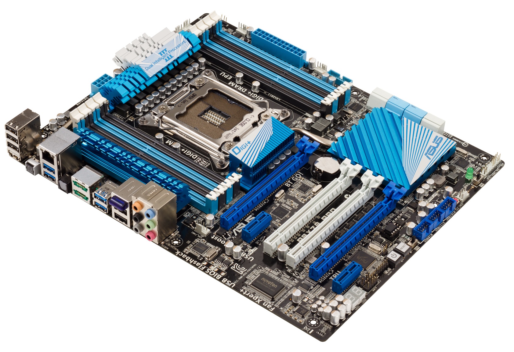
The PCH is hidden underneath a low profile heatsink, also connected via a heatpipe to another heatsink in the middle of the board. The SATA ports here on offer come in three flavors – two SATA 6 Gbps via a Marvell 9128 controller, four SATA 3 Gbps from the PCH, and two SATA 6 Gbps from the PCH. These final SATA 6 Gbps are the ones used in ASUS’ SSD Caching, explained later.
Along the bottom of the board are features of interest: a 2-digit Debug LED panel; large power/reset buttons; a small Clear CMOS; ASUS’ TPU (Turbo) and EPU (Power Saving) switches; and a standard variety of USB and front panel headers. I’m glad that the Clear CMOS button is of a different style to the power/reset buttons and not next to them – there are some boards which have it next to them, which makes for interesting expletives when the wrong button is pressed.
PCIe layout is not that intuitive, though a user should fill up the blue x16 slots first from top to bottom, then the white. As a result, we have a PCIe x16, x1, x8, x8 (non-GPU), x16, x1. The second blue x16 reduces to x8 when the first white x8 is populated. This layout also means that any PCIe x1 users will have to use the white PCIe lanes when two dual-slot GPUs are being utilized. As I mentioned previously, having such a large gap between the blue x16 slots can be an issue, when GPU manufacturers do not provide long enough cables with their cards. While ASUS provide a long enough SLI cable for this, they do not give any CrossFireX cables.
The back panel feels slightly empty here, but that may be indicative of X79 as a whole with some legacy connectors now no longer being used. From left to right, we have four USB 2.0 ports (including one in white for BIOS Flashback), a BIOS Flashback button, two USB 3.0 ports below an Intel Gigabit Ethernet port, an optical S/PDIF output, two ‘Power’ eSATA 6 Gbps ports, two USB 3.0 ports, two USB 2.0 ports below a Bluetooth v2.1 module, and standard audio headers. Personally, I see room for another Gigabit Ethernet port, hopefully with the option of Teaming.
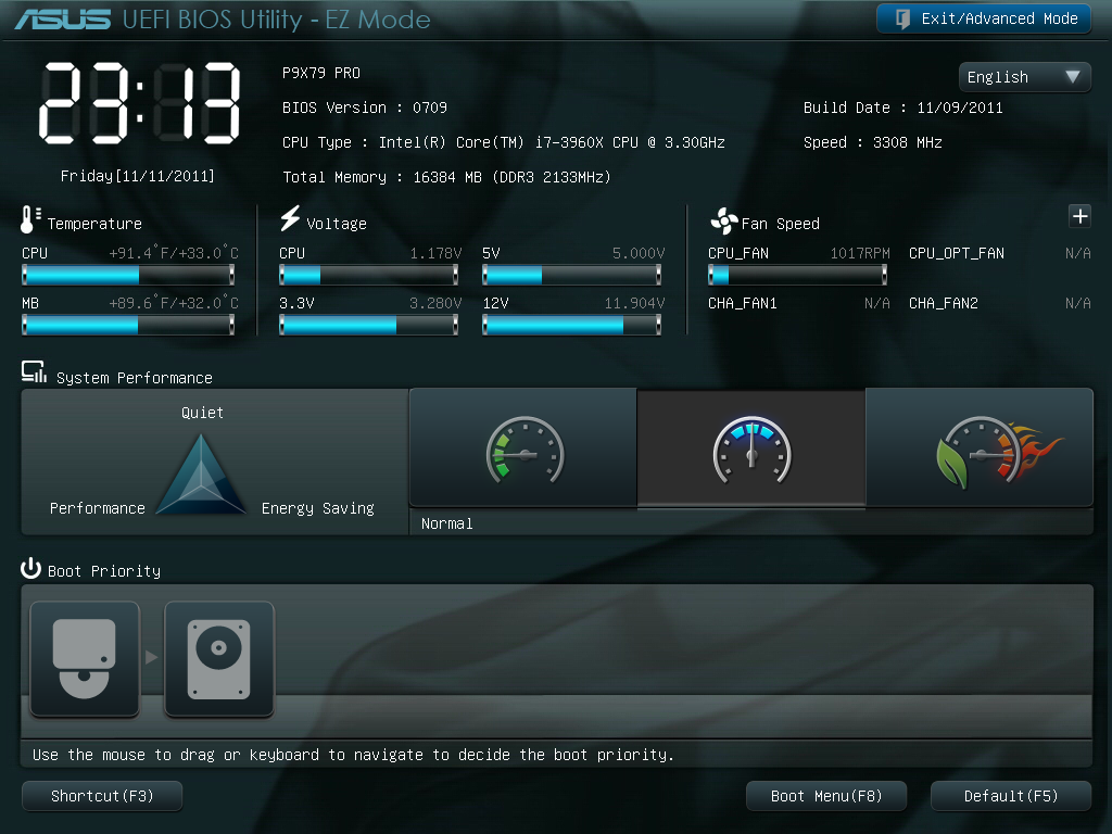
Over the past year, ASUS have built a solid graphical UEFI interface which, personally as a reviewer, covers almost everything I want in a BIOS. Rather than break something that works, ASUS have worked a little on the implementation for X79 to improve the functionality. The main change here is the shortcut menu, found by pressing F3. Rather than requiring the user to navigate through menus and deciding what is a deeper menu or not, the most frequently used options in the BIOS are listed and are now only a click away. As a long time BIOS user, I do not find much need for this – I am fairly adept at navigating through the BIOS via keyboard at speed. However, for just wanting to flash a new BIOS (I always prefer doing it in the BIOS itself), I found it quite useful.
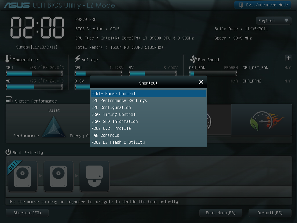
However, the user starts off in EZ mode – a simple to use screen full of information that any user or admin would want. For a start, telling us what board we are using, the processor, detected memory and speeds, CPU temperatures, voltages, fan speeds and the boot order is something every vendor should show on the front screen. ASUS has implemented this spot on. From this page, a user will be able to tell if memory is not detected, select an overall ‘faster’ or ‘greener’ mode, or arrange the boot order.
Inside the advanced mode, we have a more vintage feel of the BIOS options. Almost all the options here are selectable in a variety of ways – mouse and submenu, keyboard and submenu, or in the case of values, keyboard and typing. As a keyboard/typist sort of BIOS user, I feel frustrated when in an attempt to go graphical a motherboard manufacturer will force you to sift through a list going from 0.8 V to 1.65 V in the memory in 0.0075 V increments. There are no such problems here in ASUS’ implementation.
AI Tweaker modes come in Auto, Normal or XMP, which allows the user to define BCLK frequencies to the nearest 0.1 MHz, the CPU Strap (1.00x, 1.25x, 1.66x or 2.50x), target CPU ratios for per core usage, and the memory strap. Sub menus provide DRAM timings, where ASUS provide a seemingly endless level of detail on what users can select for their memory, control over the DIGI+ power delivery (also available in the OS), and a variety of CPU performance settings. Voltage adjustment is available underneath this, where most voltages are simple value selections, but the CPU voltage is also available in offset mode.
By pressing F5, the BIOS will revert to Intel defaults on all these values, but by pressing F6, the BIOS will default to ASUS values, which offer a change in performance. Personally, the only change I was able to discern is that this turned per core turbo ratios off, and put the i7-3960X (6C/12T, 3.3 GHz, 3.9 GHz Turbo) into a full turbo mode on any core operation. Actually, whenever I changed any part of the BIOS, this occurred. By changing any DRAM or memory timings/ratios, or setting XMP, or changing the BCLK/multiplier, rather than the CPU go into a normal mode (39x/39x/37x/37x/36x/36x ratios on 1/2/3/4/5/6 core usage), it implemented the max turbo for any CPU usage. This put a little spanner in the works regarding our benchmark suite, which as I will mention on the test setup page, I adapted the operation to standard.
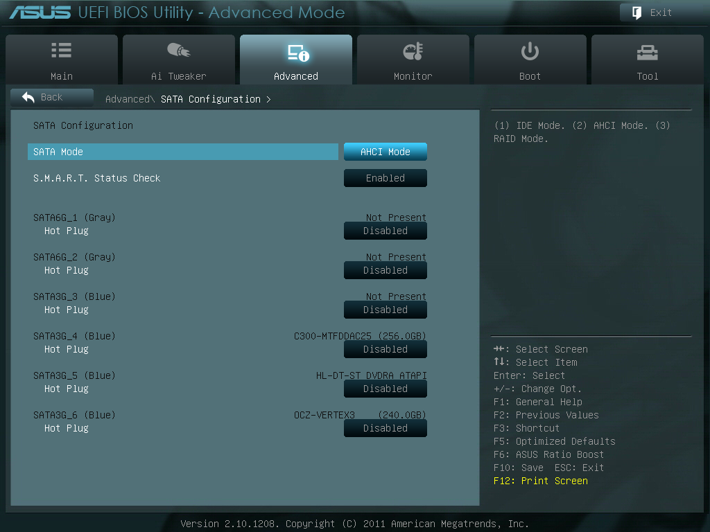
One feature I have been pushing motherboard manufacturers on for Sandy Bridge is that AHCI mode is enabled be default. So far, as much as I can tell, only ASUS on their high end products have done this. So with X79, this is the time to make the change – which ASUS have done on their Pro board, which is not their high end board. Hopefully, when looking at some of the other vendors’ implementations, they have done likewise.
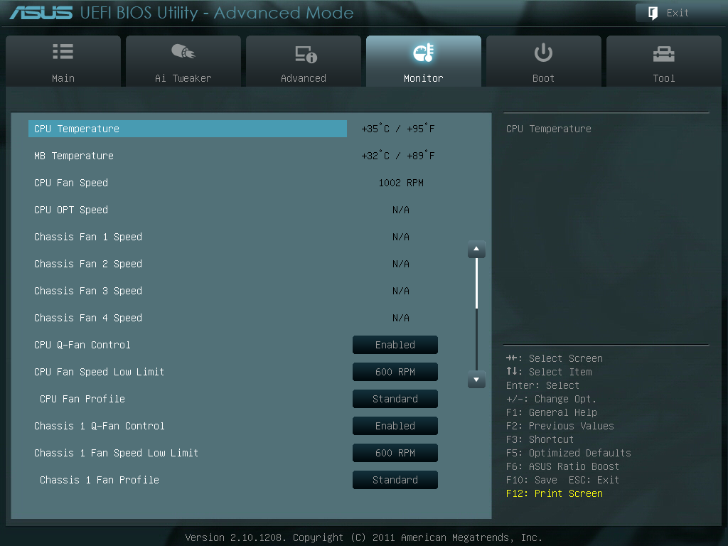
Under the Monitor heading are the BIOS fan controls, which allow almost full control over the fans (the OS software is better adapted to this). All four chassis fan headers are controllable individually, and the two CPU fan headers act under the same control.


Overclocking on X79
The realm of overclocking has changed in recent months, especially in the hands of Intel. If we take the previous enthusiast platform, X58 and LGA 1366, a full array of BCLK and multiplier adjustments were available. Personally, I moved from that platform (and my trusty i7-920 D0) to P67 and Sandy Bridge, where due to the clock generator arrangement, I had access to the multiplier and perhaps +/- 2-5 MHz on the BCLK. In terms of the joy of overclocking, this was a bit of a let down – but Intel has (sort of) met in the middle with X79.
On a basic level, we have a standard clock generator pumping out 100 MHz. This is split several ways, most notably one way to the CPU and memory through a buffer chip, and one way to everything else. Using this buffer chip, we can select four gears/ratios: 1.00x, 1.25x, 1.66x and 2.50x. As a result, we can send 100 MHz, 125 MHz, 166 MHz and 250 MHz to the CPU/memory, while restricting everything else to 100 MHz. The basic 100 MHz, like P67/Z68, can be adjusted – usually by +/- 2-5 MHz as Sandy Bridge was able. On top of all this, we also have multiplier adjustment.
With this in mind, I can already tell you that the majority of overclocks from system builders will be on the 1.25x ratio. It provides a simple 25% overclock if the multipliers are not changed, and providing they are using Intel’s all-in-one liquid cooling as a minimum (or a high end air cooler), temperatures should not be an issue. No doubt we will see motherboards that implement this as a one-button option on the motherboard – ASUS’ auto overclock option does something similar. In order to push the memory, users may opt for the 1.25x ratio, and then decrease the multiplier to a reasonable temperature level.
In terms of the ASUS’ board performance, I first had a go at the auto OC options.
Auto OC
ASUS offers a ‘Fast’ and an ‘Extreme’ mode in their software options. ‘OC Tuner’ in the BIOS, and activating the TPU switch on board, both default to the Fast mode. In this fast mode, we see a jump to the 1.25x CPU ratio, and a slight increase in the BCLK with a multiplier adjustment. Instantly, this equates to a 34x multiplier with a 126.4 MHz BCLK, giving 4296 MHz, which hits 68ºC in Cinebench (20ºC ambient max).
In Extreme mode, ASUS uses a series of algorithms and stress tests to determine the maximum frequency. Usually, I am underwhelmed by this option in my previous reviews, providing no real insight into the depth of the CPU. Despite this, the Extreme mode did run tests, BSOD and eventually reach a final speed without any intervention. A simple 35x multiplier and 127.9 MHz BCLK (4476 MHz) is good enhancement over the Fast auto OC option. However, it may worry some people that the CPU registered an 88ºC temperature when stress tested.
Manual OC
In terms of manual adjustment, my main focus here was the multiplier. Booting at 45x, with auto voltages and the CPU fan/pump set at 100%, the board was stable. However, it was pulling 1.496 V at load, resulting in 90ºC under full OCCT stress – far too hot for my liking, and this is outside a case! But setting the voltage manually to 1.4 V, the board still booted happily at 45x, giving only 82ºC under stress. The board would boot at 46x, but was unstable at 47x.
At the 46x multiplier, at 1.4 V, with load line calibration at auto, the CPU would hit 82ºC under OCCT or Blender Stress, and only 73ºC for the 3DPM multithreaded (3DPM-MT) benchmark. At this speed (4.6 GHz, 6 cores, 12 threads), our 3DPM-MT gave a score of 1145.66, up from 914.76 at stock.
Memory
Of note with this BIOS (0709), is that when I populated the memory slots with 4x4GB DDR3, the board would default to the nearest JEDEC speed timings of the kit to 1600 MHz – in this case, my G.Skill kit has a JEDEC of 1676 MHz at 11-11-11, so the board defaulted to 1600 11-11-11. When I selected 1866 MHz memory, it shifted to 9-9-9, disregarding JEDEC vales.
The XMP profile was easy enough to enable with the XMP mode. For more performance, I pushed the board on to the 2400 MHz strap, which booted at auto values of 10-11-10 2T, and was completely stable. Moving towards the 2666 MHz strap caused failed boots. The nearest strap while on the 1.25x ratio was only at 2333 MHz, suggesting that 2400 MHz on the 1.00x strap is a safe memory overclock.
Board Features
| ASUS P9X79 Pro | |
| Size | ATX |
| CPU Interface | LGA2011 |
| CPU Support | Intel Second Generation Core i7 Sandy Bridge-E |
| Chipset | Intel X79 |
| Base Clock Frequency | 100.0 - 100.3 MHz |
| Core Voltage | Auto, offset and manual, 0.8 V to 1.7 V |
| CPU Clock Multiplier | Auto, 12x to 57x |
| DRAM Voltage | Auto, 1.20 V to 1.99 V |
| DRAM Command Rate | Auto, 1T to 3T |
| Memory Slots |
Eight DDR3 DIMM slots supporting up to 64 GB Up to Quad Channel Support for DDR3, 800-2666 MHz |
| Expansion Slots |
2 x PCIe Gen 3 x16 2 x PCIe Gen 3 x8 2 x PCIe Gen 2 x1 |
| Onboard SATA/RAID |
2 x SATA 6 Gbps, Support for RAID 0, 1, 5, 10 4 x SATA 3 Gbps, Support for RAID 0, 1, 5, 10 |
| Onboard |
2 x SATA 6 Gbps (Marvell) 4 x SATA 3 Gbps (PCH) 2 x SATA 3 Gbps (PCH) w/ SSD Caching 6 x Fan Headers 1 x Front Panel Header 1 x Front Panel Audio Header 1 x S/PDIF Out Header 4 x USB 2.0 Headers 1 x USB 3.0 Header 1 x EPU Switch 1 x TPU Switch Power / Reset / Clear CMOS Buttons + Debug LED |
| Onboard LAN | Intel Gigabit 82579V |
| Onboard Audio | Realtek ALC898 |
| Power Connectors |
1 x 24-pin ATX connector 1 x 8-pin 12V connector |
| Fan Headers |
2 x CPU Fan Header 4 x Chassis Headers |
| IO Panel |
6 x USB 2.0 4 x USB 3.0 1 x BIOS Flashback Button 1 x Intel Gigabit Ethernet 1 x Optical S/PDIF Out Connector 2 x Power eSATA 6 Gbps Bluetooth v2.1 Audio Jacks |
| BIOS Version | 0709 |
| Warranty Period | 3 Years |
The Intel NIC is very welcome on a high end platform, as well as one of the later models of Audio Codec by Realtek, which is represented in the DPC Latency performance. The BIOS Flashback feature (Update BIOS via USB without CPU or DRAM) is an excellent feature I hope ASUS ports to all future chipsets, as well as the SSD Caching option even though it is not part of the X79 specifications. Six fan headers is always good, as well as Debug LED and power/reset buttons, however as mentioned previously I would have liked another Ethernet port.
As always, ASUS motherboards have a 3 year warranty.
In The Box
IO Shield
Manual
Driver CD
1 x Long SLI Cable
1 x Rigid Tri-SLI Connector
6 x SATA cables, locking, right angled
Q-Connectors
While ASUS have spent money on the cables and the SLI connectors, on a product at this price, I would have liked to see a long CrossFireX cable and a USB 3.0 front bracket.
Software
Software installation, as always with ASUS, is straightforward. Clicking Install-All on the CD menu under the Driver section does the drivers, and then once again under the Software for software. ASUS bundles Google Chrome and Norton Antivirus with the CD as well which annoyingly ask to be installed – users have to deselect them if they do not want them. Daemon Tools Pro is also on the CD, though users have to install it individually.

The main stalwart of ASUS software is still here, under a slightly redesigned ASUS AI Suite II. With the depth of X79 and all the new features ASUS have added, we have to get to grips with the whole software. Overclocking function is nothing spectacular here, with Auto Tuning and slider adjustment being identical to previous implementations. With the advent of DIGI+ VRM for the memory, we now get options to adjust this, as well as the DIGI+ for the CPU.
Energy efficiency options also get a revamp in their modes, and in terms of fan controls, each of the four chassis fan headers are double-ramp adjustable, and the two CPU fan headers act under the one control.
The two new areas of ASUS brand technology come in the form of ASUS USB 3.0 Boost, and ASUS SSD Caching. Let us go over each one in turn.
ASUS USB 3.0 Boost
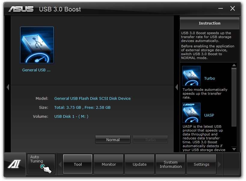
Readers of this year’s content may cast their minds back to the several ASRock boards I have reviewed, and their XFast USB software. This was a simple bit of software that modified and optimized the Windows7 USB driver to allow for faster operation. ASUS have gone in a similar theme, but taken it several steps further.
On the simple end, there are multiple USB protocols to use. Windows, by default, uses BOT – a simple linear process protocol for file transfer. By a simple rewrite of the driver, such as the ASRock implementation, a motherboard manufacturer can implement a ‘Turbo’ mode, which acts like a more multithreaded environment.
Now, if the USB device or enclosure has certain classes of controllers (LucidPORT USB300-REV2, ASMedia ASM1051E, ASMedia ASM1051U, ASMedia ASM1054), a protocol known as UASP (USB Attached SCSI Protocol) can be implemented. This protocol is more efficient, and allows multiple, concurrent commands, rather than the linear BOT sequence. This is what USB 3.0 Boost is aimed at.
Initially, each USB 3.0 device will need to be set to Turbo or UASP as required, but devices are remembered for repeat use. Unfortunately, I do not have access to a device to test this UASP performance; however I was able to see it in action at a recent ASUS event.
ASUS SSD Caching
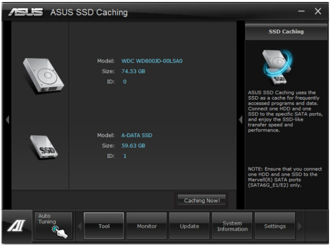
Users of Intel’s Z68 Smart Response Technology that were dismayed when SRT was not a part of the X79 specifications will be overjoyed to see something similar to Intel’s operation on ASUS’ X79 range. By placing two compatible drives (typically a mechanical HDD and a formatted SSD) in the appropriate SATA ports, the software and hardware implementation will let the SSD act as a cache, in order to improve loading times to the mechanical HDD, just like Intel’s RST.
The potential here is possibly using any extra RAM as a cache. With the abundance of 4x4GB kits for use in such a system, from my own personal experience, almost half of that would never be used – the most memory I’ve ever used is 7.9 GB, which included a hundred or so internet tabs, background software, and whilst playing F1 2010 at full settings. If ASUS were to license a RAMDisk software technology to allow users to create a RAMDisk, and then use that in an SSD caching technique, then we are on to a winner. Even better if a user has decided to fill up the memory slots with 32 GB. Admittedly, this would be lost every time the system is rebooted, and would have to be remade, but for users who leave their system on all the time for various reasons, it could provide useful.


Test Setup
| Processor |
Intel Sandy Bridge-E i7-3960X 6 Cores, 12 Threads, 3.3 GHz (3.9 GHz Turbo) |
| Motherboards | ASUS P9X79 Pro |
| Cooling | Intel All-In-One Liquid Cooler, made by Asetek |
| Power Supply | Silverstone 1000W 80 PLUS Silver |
| Memory | G.Skill RipjawsZ DDR3-2133 9-11-9 28 4x4 GB Kit 1.65V |
| Memory Settings | XMP (2133 9-11-9-28 2T) |
| Video Cards | XFX HD 5850 1GB |
| Video Drivers | Catalyst 11.8 |
| Hard Drive | Micron RealSSD C300 256GB |
| Optical Drive | LG GH22NS50 |
| Case | Open Test Bed - CoolerMaster Lab V1.0 |
| Operating System | Windows 7 64-bit |
| SATA Testing | Micron RealSSD C300 256GB |
| USB 2/3 Testing | Patriot 64GB SuperSonic USB 3.0 |
Due to the ASUS BIOS implementing a 39x multiplier when XMP is selected, for testing we have manually set the Per Core CPU ratios to Intel Specifications for true comparison – otherwise the P9X79 Pro would score more on the multithreaded scenarios due to a pure MHz advantage.
G.Skill have come up trumps again by sending us one of their premium RipjawsZ kits (F3-17000CL9Q-16GBZHD). This quad channel 16 GB kit comprises of four modules with an XMP rating of DDR3-2133 9-11-9-28 at 1.65 V. Due to the ‘ZHD’ at the end, it is geared for high-performance, tight timings, and comes with two active coolers.


Power Consumption
Power consumption was tested on the system as a whole with a wall meter connected to the power supply, while in a dual GPU configuration. This method allows us to compare the power management of the UEFI and the board to supply components with power under load, and includes typical PSU losses due to efficiency. These are the real world values that consumers may expect from a typical system (minus the monitor) using this motherboard.
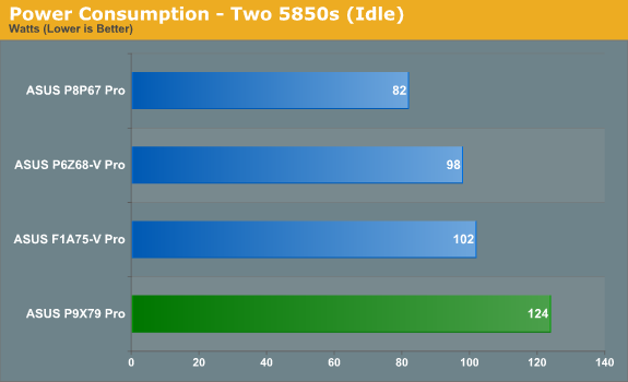
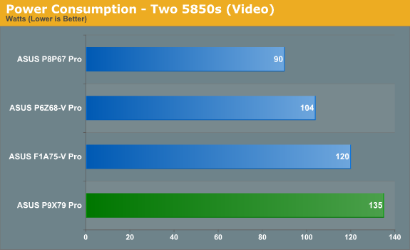
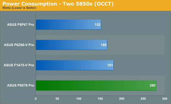
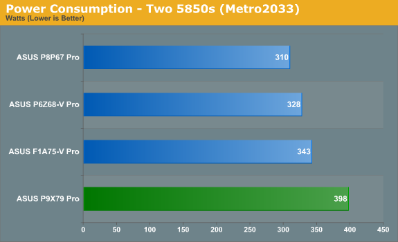
In comparison to boards I have tested this year, overall power consumption at the wall is increased signicantly, primarily due to the CPU being rated at 130 W, compared to the 90-95W parts such as the i5-2500K on P67/Z68 and the A6-3650 on A75.
CPU Temperatures
With most users running boards on purely default BIOS settings, we are running at default settings for the CPU temperature tests. This is, in our outward view, an indication of how well (or how adventurous) the vendor has their BIOS configured on automatic settings. With a certain number of vendors not making CPU voltage, turbo voltage or LLC options configurable to the end user, which would directly affect power consumption and CPU temperatures at various usage levels, we find the test appropriate for the majority of cases. This does conflict somewhat with some vendors' methodology of providing a list of 'suggested' settings for reviewers to use. But unless those settings are being implemented automatically for the end user, all these settings do for us it attempts to skew the results, and thus provide an unbalanced 'out of the box' result list to the readers who will rely on those default settings to make a judgement.
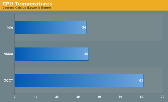
Despite using Intel's liquid cooler for this test, the temperature difference during OCCT is astounding for this platform. It's good to see little change between Idle and Video temperatures, however.
USB Speed
For this benchmark, we run CrystalDiskMark to determine the ideal sequential read and write speeds for the USB port using our 64GB Patriot SuperSpeed USB 3.0 drive. Then we transfer a set size of files from the SSD to the USB drive, and monitor the time taken to transfer. The files transferred are a 1.52 GB set of 2867 files across 320 folders – 95% of these files are small typical website files, and the rest (90% of the size) are the videos used in the Sorenson Squeeze test.
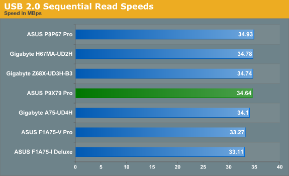
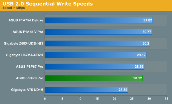
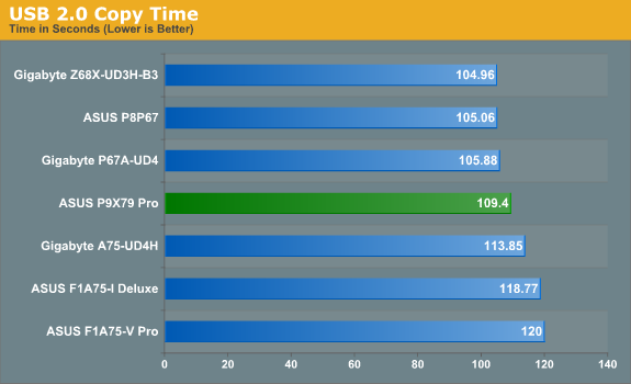
Unfortunately, we ran into an issue with our USB 3.0 stick after the USB 2.0 tests. For some reason it is no longer being detected properly. When we get a replacement, the graphs shall follow.
SATA Testing
We also use CrystalDiskMark for SATA port testing. The operating system is installed on the Micron RealSSD C300, which is rated at 355 MB/s read and 215 MB/s write, and the sequential test is run at the 5 x 1000 MB level. This test probes the efficiency of the data delivery system between the chipset and the drive, or in the case of additional SATA ports provided by a third party controller, the efficiency between the controller, the chipset and the drive.
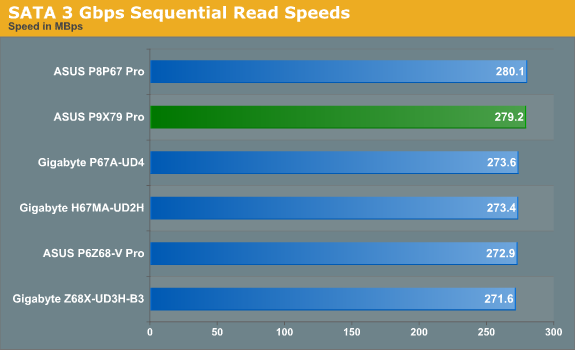
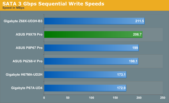
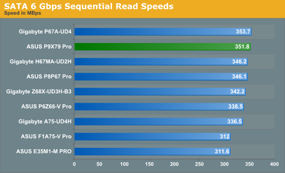
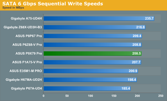
Overall, the PCH does well in SATA sequential speeds compared to previous platforms.
DPC Latency
Deferred Procedure Call latency is a way in which Windows handles interrupt servicing. In order to wait for a processor to acknowledge the request, the system will queue all interrupt requests by priority. Critical interrupts will be handled as soon as possible, whereas lesser priority requests, such as audio, will be further down the line. So if the audio device requires data, it will have to wait until the request is processed before the buffer is filled. If the device drivers of higher priority components in a system are poorly implemented, this can cause delays in request scheduling and process time, resulting in an empty audio buffer – this leads to characteristic audible pauses, pops and clicks. Having a bigger buffer and correctly implemented system drivers obviously helps in this regard. The DPC latency checker measures how much time is processing DPCs from driver invocation – the lower the value will result in better audio transfer at smaller buffer sizes. Results are measured in microseconds and taken as the peak latency while cycling through a series of short HD videos - under 500 microseconds usually gets the green light, but the lower the better.
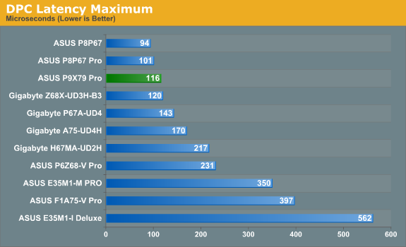
As with the faster processor, we are expecting better DPC Latency as long as the system is engineered quickly. Our max result here was 116 microseconds, however this was a blip - for most of the time, the board would hover around 30 microseconds, which is an excellent result.
3D Movement Algorithm Test
The algorithms in 3DPM employ both uniform random number generation or normal distribution random number generation, and vary in various amounts of trigonometric operations, conditional statements, generation and rejection, fused operations, etc. The benchmark runs through six algorithms for a specified number of particles and steps, and calculates the speed of each algorithm, then sums them all for a final score. This is an example of a real world situation that a computational scientist may find themselves in, rather than a pure synthetic benchmark. The benchmark is also parallel between particles simulated, and we test the single thread performance as well as the multi-threaded performance.
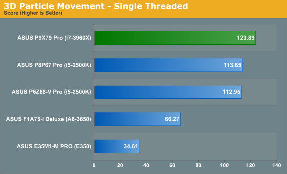
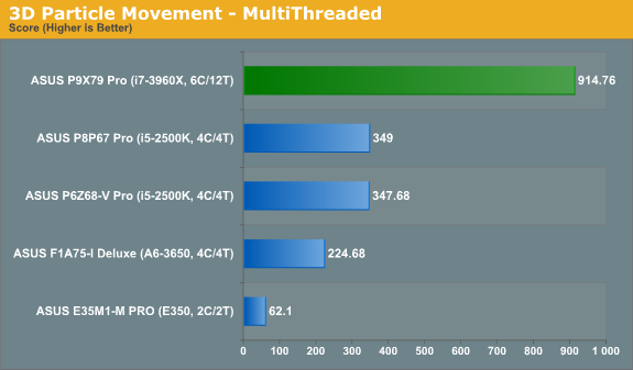
As expected, due to the 3960X, we have a clear lead on 3DPM. In single thread mode, we have a 3.9 GHz core taking top place, and the power of 12 threads at 3.6 GHz in multithreaded mode shows in the 914.76 score.
WinRAR x64 3.93 - link
With 64-bit WinRAR, we compress the set of files used in the USB speed tests. WinRAR x64 3.93 attempts to use multithreading when possible.
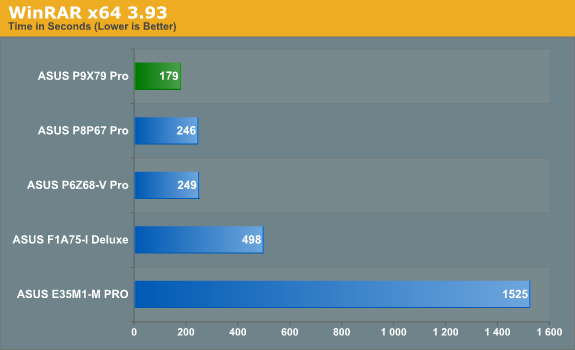
The more cores and threads for WinRar also play a role in providing some excellent times in comparison to other chipsets.
FastStone Image Viewer 4.2 - link
FastStone Image Viewer is a free piece of software I have been using for quite a few years now. It allows quick viewing of flat images, as well as resizing, changing color depth, adding simple text or simple filters. It also has a bulk image conversion tool, which we use here. The software currently operates only in single-thread mode, which should change in later versions of the software. For this test, we convert a series of 170 files, of various resolutions, dimensions and types (of a total size of 163MB), all to the .gif format of 640x480 dimensions.
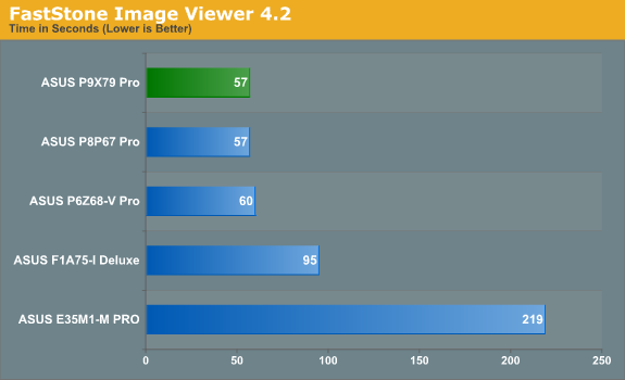
In this single threaded workload, no real difference is seen compared to P67, showing that for FastStone, memory is not a limiting factor, and the move to SB-E doesn't make much of a difference.
Sorenson Squeeze 6.0 - link
Sorenson Squeeze is a professional video encoder, complete with a vast array of options. For this test, we convert 32 HD videos, each a minute long and approximately 42 MB in size, to WMV 512KBps format. Squeeze can encode multiple videos at once, one for each thread.
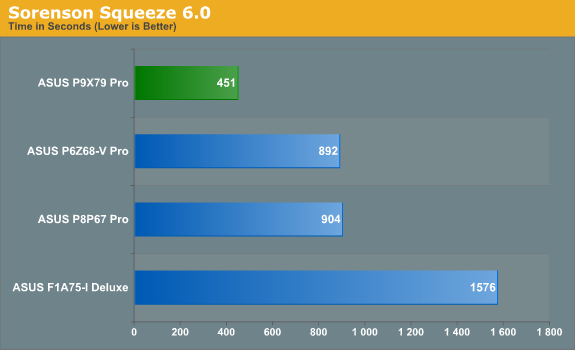
With Squeeze being a fully multithreaded test, we're comparing a 4 thread i5-2500K to a 12 thread 3960X, so it's no wonder that the 3960X comes out on top.
Aliens vs. Predator Benchmark
Aliens vs. Predator is a DirectX 11 science fiction first-person shooter video game, developed by Rebellion Developments. Available as a standalone benchmark, on default settings the benchmark uses 1920x1080 with high AF settings. Results are reported as the average frame rate across 4 runs.
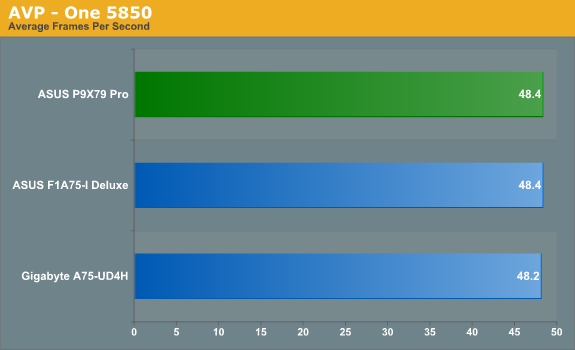
Nothing splits AVP with one 5850, showing that this is primarily a GPU limited game.
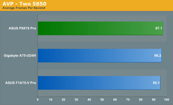
Using two 5850s, we start to see a small difference - showing that the increased bandwidth to the second GPU has an effect on the results.
Dirt 3
Dirt 3 is a rallying video game and the third in the Dirt series of the Colin McRae Rally series, developed and published by Codemasters. Using the in game benchmark, Dirt 3 is run at 1920x1080 with full graphical settings. Results are reported as the average frame rate across 4 runs.
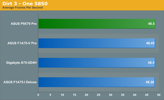
Similarly in Dirt 3's single 5850 results, all the values are within statistical variance, and that the CPU is not the limiting factor here.
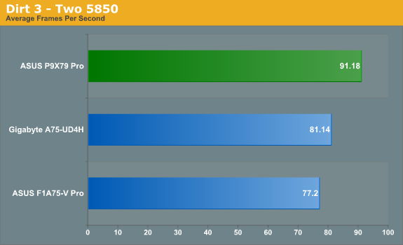
However, in dual GPU mode, the increased bandwidth to the second GPU has a startling affect on the frame rates, making an x16/x16 layout beat an x8/x8 by over 10 FPS. The x16/x4 of the F1A75-V Pro distinctly lags behind.
Metro2033
Metro 2033 is a challenging DX11 benchmark that challenges every system that tries to run it at any high-end settings. Developed by 4A Games and released in March 2010, we use the inbuilt DirectX 11 Frontline benchmark to test the hardware at 1920x1080 with full graphical settings. Results are given as the average frame rate from 10 runs.
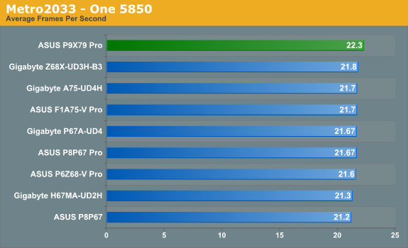
Having had Metro2033 part of the motherboard GPU suite for a while, we have more results to draw from. In single GPU mode, we only see a 1 FPS difference between all the chipsets, showing that the GPU is still the limiting factor here.
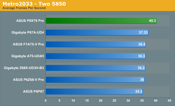
However, in dual GPU mode there is a significant leap when X79 is used, All the other results are fairly similar, coming from A75 and P67/Z68, showing that the CPU hasn't made much of a difference, but the x16/x16 layout of the PCIe slots on the P9X79 Pro gives a clear 3-4 FPS improvement.
Final Words
With a new enthusiast platform, it is easy to get caught in the hype of just how well a processor is when analyzing a motherboard. Part of my job is to communicate what I think about the motherboard to the readers and hopefully provide information as well as a judgment on the product at hand.
So this review has been about X79, and specifically ASUS’ P9X79 Pro. If the past has told us anything, the Pro boards from ASUS have been hot sellers, and I expect X79 will be no different, assuming users will also shell out for the Sandy Bridge-E processors. The P9X79 Pro is expected to retail at $329.99 on release, which to a lot of non-enthusiast users will seem mind blowing that a motherboard could cost this much. But there is method in the madness.
From the outside, as a whole, X79 contains a lot of what an enthusiast user may want from a motherboard – lots of memory channels and lots of PCIe lanes for GPUs being the main plus points here. Downsides are the lack of USB 3.0 native support, the promise of SAS support being removed, no Z68 RST, and the persistence of SATA 3 Gbps ports on Intel’s PCH when AMD can provide six SATA 6 Gbps ports from their FCH.
ASUS have tried to change that, by introducing sets of unique features to the platform. Their SSD caching technology is a welcome side to the platform, USB 3.0 Boost offers that little bit extra beyond the standard X79 specifications from the USB, and BIOS Flashback technology is an ideal feature that in retrospect should have been on motherboards years ago. The board as a whole gives a clear indication of what can be possible after Intel hands a motherboard manufacturer a chipset and the chipset specifications.
Alongside the board’s aesthetics, we have a well featured product on our hands. The P9X79 Pro has six fan headers, all under some of the best controls available on a motherboard; power/reset/clear CMOS buttons; a debug LED; ASUS’ DIGI+ VRM solution for fine tuning; ASUS’ TPU (Turbo) and EPU (Power Saving) processors; a BIOS full of features especially when tuning memory; Bluetooth; and an Intel NIC.
No board has ever been perfect, and the nit picking I have to do here is relatively minor. The ‘per-core’ adjust required for fairness in comparison to other boards was a little peculiar, and in terms of what came with the board, I would have preferred a CrossFireX cable rather than one of the SLI cables, to account for the spacing between the first two recommended GPU slots. At ~$330, a USB 3.0 front panel may have been a good addition too, as well as another NIC.
Hopefully a lot of people who buy this board will enjoy it as much as I have enjoyed reviewing it. For this, I would like to give ASUS, and the P9X79 Pro, a silver AnandTech Editors’ Choice award, for innovation on such a solid product beyond the standard specifications, as well as having the solid hardware and software backbone that users expect in a motherboard.