Original Link: https://www.anandtech.com/show/998
Inside ATI & NVIDIA: How they make frames fly
by Anand Lal Shimpi on September 23, 2002 2:14 AM EST- Posted in
- GPUs
Ever since we started our Inside series the two companies we've received the most requests for have been ATI and NVIDIA. After touring Intel's research labs in Oregon and visiting VIA in Taiwan, we felt it was time to visit the two kings of graphics - ATI and NVIDIA.
We combined these two companies into one article for one reason in particular - our tours were complementary. ATI imposed very strict restrictions on photographs during our visit to their offices in Thornhill, Ontario; we saw a lot of interesting things at ATI's offices (including the foundation for their fountain of fire in the lobby of their main building) but we weren't able to take pictures of most of them. On the other hand, ATI sat us down with one of their chip architects and we were able to get a wealth of information about how their GPUs were made.
NVIDIA wasn't able to set us up with any engineers for an extended period of time (although lunch with Chief Scientist, David Kirk is always informative) but they were much more lax on the picture front so we were able to bring you more of the behind the scenes from NVIDIA.
The combination of the two visits provided us with enough material to put together this piece, so without further ado let's take you inside ATI and NVIDIA.
Inside ATI - Designing a Chip
We've often been asked how exactly these graphics giants go about doing what they do, and that's exactly what we asked an ASIC engineer at ATI to help us explain.
The first step in GPU design is of course, marketing; a spot will be defined in the market, where the product will end up being aimed at. A document describing this gets served to a lead architect where details such as costs, schedules and resources required are discussed.
The cost limitations also help determine figures like transistor counts; at this stage the target manufacturing process is also chosen depending on a number of factors. As you can expect the manufacturing process (e.g. 0.15-micron, 0.13-micron, 90nm, etc…) contributes to the cost structure of the chip and imposes die sizes/transistor count limitations as well. What's important to note is that the target manufacturing process is decided upon at the very start of the design cycle based on estimates of where the foundry (the people that actually manufacture the chip - e.g. TSMC) will be at by the completion date. If this estimate is off, which was the case with NVIDIA's NV30 design, then the GPU will be inevitably delayed. Once a manufacturing process is decided upon, it is extremely difficult to, months later, go back and attempt to revise the design for a different process.
Discussions will continue between the designers and the marketing team for a matter of weeks. The process works much like a loop, with the designers revising documents sent to them by the marketing folks and so on and so forth.
Once a product cost and schedule is decided upon, it's time to start building the architecture. A team of engineers is roundup up and they start defining the features of the GPU, who will be working on them as well as defining the design schedule (e.g. Team 1 - have antialiasing unit completed in three weeks). Before we get to the actual designing you have to understand a bit of how you actually make a chip.
These days, chip architecting has been made infinitely easier through the advent of Hardware Description Languages (HDLs). A HDL, as the name implies, is a type of programming language that effectively describes hardware. Using a HDL such as Verilog or VHDL (two common HDLs), a designer would write code that is translated by a synthesizer into a netlist or schematic that can be used to produce a chip from. Thus when designing actually begins, there's a bit of circuit diagramming but mostly a lot of code-writing. Keep in mind that programming in these HDLs is absolutely nothing like programming in C or C++. While the code may look very similar to C, the actual functionality is very different. Let's take a very basic example from Verilog:
always@(posedge clock)
Q <= D;
The above code executes whenever there's a rising edge on the clock; when it does execute, the input signal 'D' is stored in 'Q'. We've effectively designed a very basic form of memory using a storage element known as a flip-flop. A synthesizer would take this code and produce a circuit based on the hardware that this code describes; in this case it would produce a storage element that would retain the value of its input.
Using their skills, the team of engineers would then code and design the chip and all of its units in a HDL, like Verilog, for around 3 to 4 months (depending on the scale of the project). During these months of coding, all of the features decided upon earlier are now implemented into the actual chip itself.
After the design is completed the next few months are spent in verification. The process of verification is critical to meeting production schedules because it helps get rid of problems before the chip is actually sent to the foundry for production. If a chip comes back from the foundry and it turns out that the design doesn't work as planned, then you've not only wasted a good deal of time but also an incredible amount of money.
Part of the verification process entails basic functionality tests to make sure that all of the gates within the chip work properly. Workloads are also simulated to make sure that the gates not only work but they also work as expected. Some of these tests are also conducted through the HDL itself by writing programs to test the hardware (sort of simulating a tester as well as the chip itself).
At this point one team will branch off and begin some static timing analysis to make sure that the chip will be able to meet clock speed goals. Remember that even at this point there is no physical "chip" just a simulation. While all of this is happening, a team of analog engineers is working on the memories, power circuitry, etc… Analog design and engineering is a very complex and dramatically different beast from the digital logic that we've been talking about until this point, there's a strong focus on understanding the elements of complex numbers, differential equations and signal analysis. The analog portion of the equation cannot be ignored as it's a very important part of the GPU design and manufacturing process; luckily the digital designers don't have to mess with it too much.
Finally, after all of the testing the chip is "synthesized" meaning that the HDL is translated into a gate-level netlist or schematic that is used to physically manufacture the chip. The first cut placement route is done, which is the real layout or how the gates will look in silicon. At this point there's still no chip to play around with but the chip can be "produced" using what is known as a FPGA (Field Programmable Gate Array).
 A
FPGA is a generic logic device consisting of a large number of gates; the gates
can be configured in such a way to effectively emulate the chip before production.
The benefit of doing this is that the chip can be fully tested and operational
for only the cost of the FPGA which is on the order of thousands of dollars,
whereas it costs millions to get a chip to and back from a foundry. A particular
type of FPGA is used by both ATI and NVIDIA and it's manufactured by a company
called IKOS; the IKOS box, as it is often referred to, is effectively a very
large FPGA used to emulate designs like the R300 or NV30.
A
FPGA is a generic logic device consisting of a large number of gates; the gates
can be configured in such a way to effectively emulate the chip before production.
The benefit of doing this is that the chip can be fully tested and operational
for only the cost of the FPGA which is on the order of thousands of dollars,
whereas it costs millions to get a chip to and back from a foundry. A particular
type of FPGA is used by both ATI and NVIDIA and it's manufactured by a company
called IKOS; the IKOS box, as it is often referred to, is effectively a very
large FPGA used to emulate designs like the R300 or NV30.
The IKOS box can fully emulate a design however it isn't able to run anywhere near as fast as the final GPU will operate. While today's GPUs are running at speeds above 300MHz, the IKOS box can emulate the design running at a small fraction of that - in the KHz frequency range (1000 KHz = 1 MHz). With the GPU running that slowly, you can't gauge performance but you can run a system with the OS installed, test drivers, and even run games on the IKOS box (albeit at ~0.2fps).
After the verification process is complete and the layout is done then comes the elusive tape-out. This is the preparation of everything necessary to be sent out to the foundry for actual production of the chip. About 4 weeks later you get your first chip or A0 silicon as it is often referred to as. The testing doesn't stop during those four weeks however, simulations continue as well as verification of the PCBs (Printed Circuit Boards) that the GPU will eventually be soldered onto.
Once the first silicon (A0) is back verification of it starts immediately; all of the functional units are tested and any unexpected behavior is immediately noted and debugged. Focused Ion Beam (FIB) tools are sometimes employed to fix bugs in the chip; we introduced the concept of using a FIB tool in our Inside Intel article, but as a brief refresher, a FIB tool allows you to effectively perform surgery on a microprocessor without ruining the functionality of the chip. The tool allows you to cut or lay down new wires on a chip, down multiple metal layers, to fix a bug in the design without destroying the chip. This way ATI or NVIDIA can attempt to fix a bug and see whether the bug is actually fixed before sending the revised design back to the foundry; remember it takes about 4 weeks to get a chip back after tape-out and you don't want those 4 weeks to be wasted if it turns out that the fix doesn't really get rid of the bug.
Once all of the bugs are fixed the finalized design is taped-out and sent to the foundry for production. These chips are then sent through qualification where they are put through all sorts of tests for compatibility, thermal and voltage stresses, signal integrity, etc…
After qualification is complete, it's time for production and now you know how GPUs are made.
Inside NVIDIA - The Santa Clara Tour
NVIDIA's new campus in Santa Clara, CA is impressive to say the least but at the same time, exactly what you'd expect from the leader in the graphics world.

Click to Enlarge - One of NVIDIA's buildings in Santa Clara
We started off our tour revisiting NVIDIA's server farms, a site we had seen one year ago when we first walked around the new buildings. These server farms are used mostly for simulation of hardware (flip back a couple of pages to get an understanding of how) and thus the hardware demands are very high; you need a lot of memory and a lot of processing power.
NVIDIA found themselves in an interesting situation where they had no idea which platform would end up being the fastest yet most economical solution for their hardware simulation applications; NVIDIA's solution was to essentially, buy one of everything. Thus we found everything from Sun boxes to Itaniums to Pentium 4s running in their racks; the hardware that performed the best, NVIDIA bought more of and what didn't work quite as well sat there alone.

A couple of IBM boxes were found while we rummaged through NVIDIA's racks
Click to Enlarge

One of the more impressive setups was this collection (above) of 11 Sun Microsystems SunFire 6800 racks; each one of these racks has 196GB of memory courtesy of the platform's 64-bit memory addressability and costs around $1M.

The racks themselves are around 6 feet tall as you can tell by the below picture of our own Evan Lieb (AT Motherboard Editor) standing next to one:

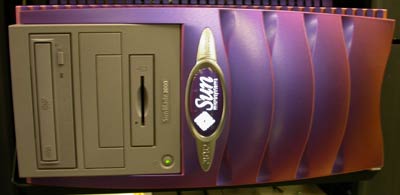
NVIDIA is currently evaluating migrating to racks of SunBlade systems as opposed to the larger SunFire 6800 setups and thus we found a couple of these boxes laying around:
NVIDIA would love to move away from these costly Sun boxes altogether and transition to a much more affordable x86-linux platform, but the problem is finding a 64-bit x86 solution. NVIDIA is currently evaluating Intel's Itanium for use in their farm but as far as their needs go, AMD's Opteron would be a gift from God. NVIDIA is eagerly awaiting the launch of Opteron so that their dreams may be fulfilled with an affordable x86 solution that offers 64-bit memory addressability; until then, they'll have to stick with these million-dollar sun systems.

Click to Enlarge - Another Sun rack standing next to a million-dollar SunFire
6800
More Servers

We showed a picture of these linux boxes (above) about a year ago when they were all running Celeron processors, today they have all been upgraded to Pentium IIIs and provide the best balance of performance and power consumption possible using today's hardware. Remember that one of the things that must be taken into account when running this many systems constantly is that power usage needs to be managed carefully.

You may remember Racksaver from our recent Athlon MP server roundup, but we were surprised to see them in NVIDIA's server farm as well:

The 1U units are all outfitted with two motherboards per server and they can be configured with either 2 or 4 CPUs. NVIDIA's CPU of choice was Intel's Pentium 4 although the servers are offered with Athlon MP and Pentium III processors as well. We found it interesting that NVIDIA hadn't adopted any Athlon MP platforms in their server setup, a testament to AMD's poor success in the enterprise market with the Athlon MP, an area Opteron hopes to improve in; judging from NVIDIA's excitement about Opteron we can see it eclipsing the Athlon MP in the enterprise world quite easily.
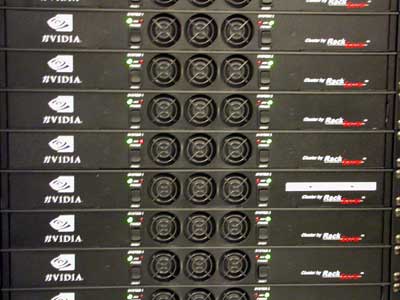
A close-up of the Racksaver racks

There are a total of 2,800 CPUs running in these Racksaver racks; the performance density offered by this 2-system/1U solution is incredible, which is why NVIDIA likes these things so much.
Storage & the rest of the Network
Storage is a very important part of NVIDIA's server farm and thus a number of racks were dedicated to storage hardware:

Each one of the cabinets pictured above were full of hard drives providing an almost unfathomable amount of storage to NVIDIA's servers. When working on design simulations of chips that are made of hundreds of millions of transistors, you not only need an incredible amount of processing power but a great deal of storage as well.

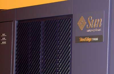
Once again we see Sun's logo, but this time as a storage server:
As you can guess, it takes a lot of skill, hard work and cabling to keep this sort of a network running and thus we have the fiber optic backbone of NVIDIA's server room:


The server room is kept surprisingly neat and well organized, impressive considering the sheer number of computers in that room.
Of course NVIDIA is always expanding, these racks will be full by the time this article is published - another 5,000 CPUs will be hard at work so you can have NV50 in a couple of years.
Of course we have to thank the serverguy for the tour, we made him late to his doctor's appointment but his help was more than appreciated.
Testing GPUs
Next up on the NVIDIA tour was one of their FA labs where manufactured GPUs and chipsets were tested.

In order to make testing a lot of GPUs easier, the video cards actually have sockets on them and the individual GPUs are just dropped into the socket. Don't get any ideas though, these sockets are only setup for use with one particular type of GPU and thus are only good for testing a bunch of the same GPU. It would be nice to have a socketed graphics card that you could upgrade down the line, unfortunately you'd need to upgrade the memory as well to keep memory bandwidth growing at the same pace as GPU speed.

An array of Quadro4 GPUs is waiting to be tested:

The socketed testing principle extends to the chipset arena as well; here we have a nForce board running through its paces. Note the socketed North Bridge:

NV30: Somewhat up and running
The IKOS lab was our next stop, where we got to see NV30 running on an IKOS box (read our Inside ATI section to learn exactly how the IKOS box works).


Click to Enlarge - It's NV30! ...but running at a few KHz and a little heavier.
The engineers were hard at work on NV30; because of the delays there has been a lot more testing and validation work on the part that should help NVIDIA considerably once all of the manufacturing issues settle. We caught a glimpse of NV30 running off of the IKOS box:

Here we have NV30 running Windows 2000:
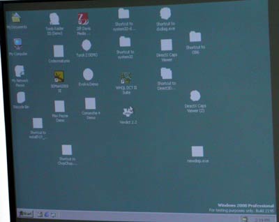
We wanted to get a game running on the IKOS NV30 but time constraints forced us to move on; plus we didn't want to impose, it's rude to play games on someone else's IKOS you know.
Probing, FIBing, & Verifying chips
Our final stop on the engineering portion of the tour took us through one of NVIDIA's low-level testing labs; these labs take silicon after they come back from the fab and are used to test the chips to make sure they function as expected. There was a good deal of equipment in this particular facility for diagnosing defects as well as implementing minor fixes through a FIB tool.

Here (above) you can see some of the probing equipment setup to diagnose low-level chip problems before sending them to the appropriate part of the lab for either further diagnostics or repairs.
This computer (below) controls the FIB (Focused Ion Beam) tool in the room; as you'll remember from our description at the beginning of this article, the FIB tool can be used to fix minor bugs on silicon without ruining the chip thus saving time and money by not forcing a new spin of the chip.

Here's the actual FIB tool itself:

Just across the room from the FIB tool was another very interesting device that is used for probing defects on a chip:

The machine pictured above will actually break down the atomic composition of any material placed in the machine. While the device inevitably gets used for things like random rocks found around on the way to work, its primary use is in finding the cause of defects. Let's take the following picture for example:

What you see on the screen is a part of a NVIDIA chip magnified at 45,000X its normal size; we've added in the box in red that encloses a defect in the chip itself. This defect could be the result of a problem during manufacturing and the way NVIDIA diagnoses exactly what caused it is by putting the chip through this machine and finding out what the atomic composition of that particular defect is. By finding out the nature of the foreign elements present at that particular point in the silicon you can then figure out what introduced the element to that part of the chip and thus help avoid future defects and improve yields.
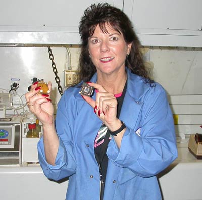
Here we have Patricia, one of the Sr. engineers at NVIDIA that works in this particular lab. In her hands she's holding two chips; in her left hand is a GPU with the top layers of the silicon dissolved and in the right hand is a piece of silicon extracted from the GPU. Below you can see a close-up of the two:

The GPU's core is dissolved using some very powerful acids that it is exposed to in order to gain access to the part of the silicon necessary for removal.

The machine above is a tool used to verify the packaged silicon by running a series of tests to make sure it works according to spec. In chip design there's an incredible amount of emphasis on verification because every bug discovered before spinning a new revision of the silicon saves time and money.
Lunch's on Jen-Hsun
It's rare that you see the CEO of a company the size of NVIDIA just walking around and interacting with the thousands of employees, but that's what we've come to expect from NVIDIA's Chief Executive Jen-Hsun Huang. We were eating at NVIDIA's cafeteria when Jen-Hsun walked by (of course cutting to the front of the line, one of the perks of being the CEO of NVIDIA) and offered to buy us lunch, apparently if you tell the cafeteria workers that Jen-Hsun is buying they just let you through - no questions asked.
Later on that day we managed to catch up with Jen-Hsun in his cubicle and talked to him for a bit:

Just like many of today's Silicon Valley CEO's, Jen-Hsun works in a cubicle just like the rest of the employees at NVIDIA. We talked with Jen-Hsun a bit about the future of nForce2; he felt that with AMD's 2003 shipments being mostly Athlon XPs (supposedly around 60% Athlon XPs vs. 40% Hammers by Q4-03), nForce2 would have a good chance to succeed.
What does NVIDIA's CEO have laying around his cubicle? Other than the pictures of his family he had a handful of NVIDIA GPUs and cards:


This Riva TNT card (above) is actually running a peltier cooler and was among Jen-Hsun's toys.

What started it all, the NV1 from NVIDIA (above). This card, the Diamond Edge 3D retailed for $249 and came with 1MB of VRAM (you could get a whopping 2MB of VRAM as well). The card came bundled with Virtua Fighter Remix and it could run the game at 800x600 at around 30 fps.


Both of these posters can provide a few laughs, and we'll end on the number one reason to invest in NVIDIA:

Final Words
We hope you enjoyed this continuation of our Inside series; we've got many more companies to take you behind the scenes of but until then be sure to check out our previous pieces on Inside Intel and VIA:
Inside Intel: From Silicon to the World
Inside VIA: Beneath the Hull of WenChi's Ship


