Original Link: https://www.anandtech.com/show/9769/arm-announces-cortex-a35
ARM Announces New Cortex-A35 CPU - Ultra-High Efficiency For Wearables & More
by Andrei Frumusanu on November 10, 2015 12:31 PM EST- Posted in
- CPUs
- Arm
- Smartphones
- Mobile
- ARMv8
- Cortex A35
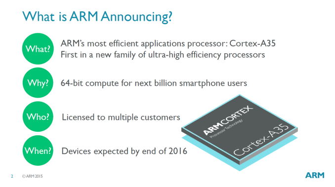
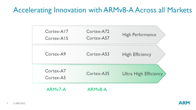
Today as part of the volley of announcements at ARM's TechCon conference we discover ARM's new low-power application-tier CPU architecture, the Cortex-A35. ARM follows an interesting product model: The company chooses to segment its IP offerings into different use-cases depending on market needs, designing different highly optimized architectures depending on the target performance and power requirements. As such, we see the Cortex-A lineup of application processors categorized in three groups: High performance, high efficiency, and ultra-high efficiency designs. In the first group we of course find ARM's big cores such as the Cortex A57 or A72, followed by the A53 in more efficiency targeted use-cases or in tandem with big cores in big.LITTLE designs.
What seems to be counter-intuitive is that ARM sees the A35 not as a successor to the A53, but rather a replacement for the A7 and A5. During our in-depth analysis of the Cortex A53 in our Exynos 5433 review earlier this year I claimed that the A53 seemed to be more like an extension to the perf/W curve of the Cortex A7 instead of it being a part within the same power levels, and now with the A35 ARM seems to have validated this notion.
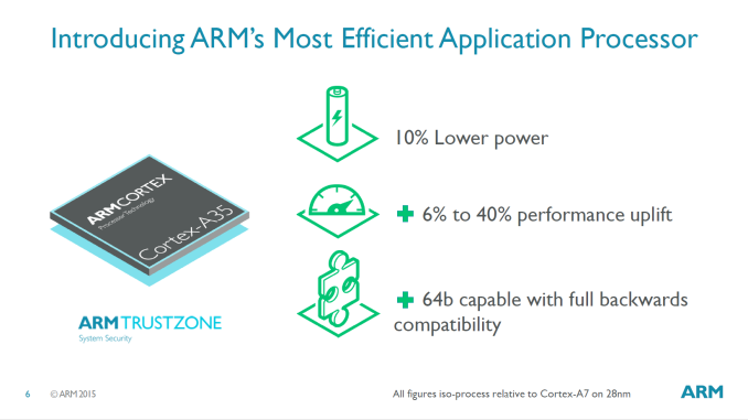
As such, the A35 is targeted at power targets below ~125mW where the Cortex A7 and A5 are still very commonly used. To give us an idea of what to expect from actual silicon, ARM shared with us a figure of 90mW at 1GHz on a 28nm manufacturing process. Of course the A35 will see a wide range of implementations on different process nodes such as for example 14/16nm or at much higher clock rates above 2GHz, similar to how we've come to see a wide range of process and frequency targets for the A53 today.
Most importantly, the A35 now completes ARM's ARMv8 processor portfolio with designs covering the full range of power and efficiency targets. The A35 can also be used in conjunction with A72/A57/A53 cores in big.LITTLE systems, enabling for some very exotic configurations (A true tri-cluster comes to mind) depending if vendors see justification in implementing such SoCs.
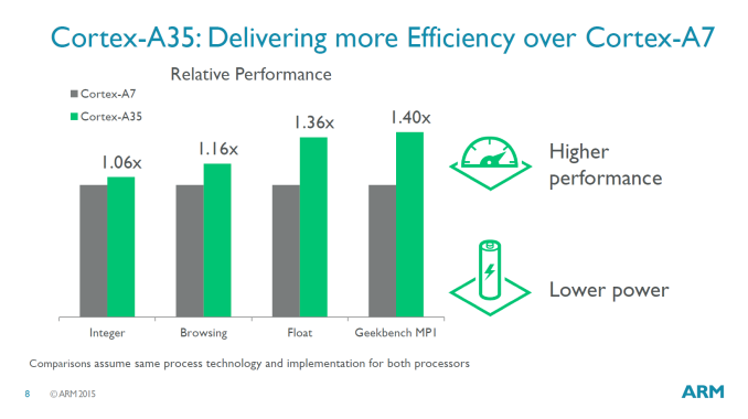
What is probably more interesting are apples-to-apples performance and power comparisons to the A53. Here the A35 actually is extremely intriguing as it is able to match the A53's performance from 80% to up to 100% depending on use-case. Browser workloads are where the A35 will trail behind the most and only be able to provide around 80% of the A53's performance. Integer workloads are quoted at coming in at 84-85% of the Apollo core, while as mentioned earlier, memory-heavy workloads are supposed to be on par with the larger bretheren.
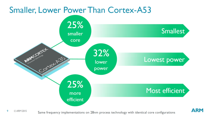
What puts things in perspective though is that the A35 is able to achieve all of this at 75% the core size and 68% the power of the A53. ARM claims that the A35 and A53 may still be used side-by-side and even envisions big.LITTLE A53.A35 designs, but I have a hard time justifying continued usage of the A53 because of the cost incentive for vendors to migrate over to the A35. Even in big.LITTLE with A72 big cores I find it somewhat hard to see why a vendor would choose to continue to use an A53 little cluster while they could theoretically just use a higher clocked A35 to compensate for the performance deficit. Even in the worst-case scenario where the power advantage would be eliminated by running a higher frequency, vendors would still be able to gain from the switch due to the smaller core and subsequent reduced die size.
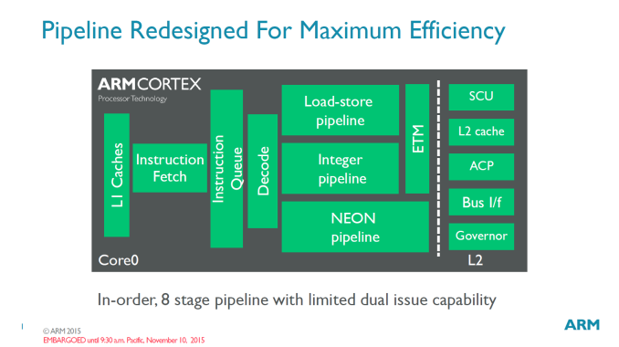
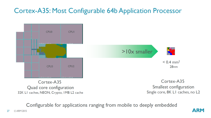
The A35 is touted as ARM's most configurable processor with vendors able to alter their designs far beyond simple choices such the core-count within a cluster. Designers will now also be able to choose whether they want NEON, Crypto, ACP or even the L2 blocks included in their implementations. The company envisions this to be processor for the next billion smartphone users and we'll likely see it in a very large variety of SoCs powering IoT devices such as wearables and embedded platforms, to budget smartphones and even high-end ones in big.LITTLE configurations.
ARM expects first devices with the A35 to ship by the end of 2016. Due to the sheer number of possible applications and expected volume, the Cortex A35 will undoubtedly be a very important CPU core for ARM that will be with us for quite some time to come.

