Original Link: https://www.anandtech.com/show/965
Almost two years ago both ATI and NVIDIA had to start making decisions about the GPUs that they would be releasing today. ATI made the decision to build R300 on a 0.15-micron process and NVIDIA was firm in their beliefs that TSMC's 0.13-micron process would be mature enough to use for Fall 2002 release of NV30.
As with any decision, the paths ATI and NVIDIA chose to go down led them through different obstacles. ATI's hybrid ATI/ArtX design team had to deal with the inevitably large die that a ~110M transistor part would have on a 0.15-micron process. To put things into perspective, this is a chip with more transistors than Intel's upcoming Prescott core, which will be built on a 0.09-micron process and a 1MB L2 cache. ATI's research told them that they would not have a mature 0.13-micron process to manufacture R300 on so they confined themselves to a 0.15-micron process, which resulted in requirements such as a 10-layer PCB and an additional power source for the Radeon 9700 Pro.
NVIDIA enjoyed the benefits of a 0.13-micron design for NV30; they could promise higher clock speeds, more features and a smaller die size than the R300 while keeping power consumption and heat dissipation down to more manageable levels. The only risks would be if NVIDIA could not get the chip design ready in time or if TSMC's 0.13-micron yields were not high enough to produce the chip in a profitable fashion.
NVIDIA wasn't the only one that had to worry about yield; the massive size of ATI's R300 would almost guarantee that yields would be low on the chip. But when push came to shove, ATI was able to introduce their R300 on time and are a matter of days away from commencing with volume shipping of the first Radeon 9700 Pro boards. ATI did find a way to balance the yield issue by allowing their partners to produce a regular version of the Radeon 9700 with a lower core clock instead of the 325MHz clock of the Radeon 9700 Pro.
This leaves us with a very important question: where is NV30? There has been a lot of speculation about NV30 and with the chip finally taped-out we're able to shed some light on the topic of NVIDIA's next-generation GPU.
What is NV30?
Before we talk about when NV30 will arrive and what's held it back, what do we know about NV30? Facing increasing competition from ATI and perceived competition from Matrox, NVIDIA divulged NV30's specifications very early on; even before Parhelia's retail launch.
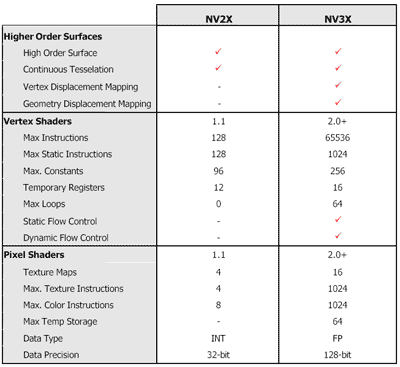
Publicly there's not much we can tell you about NV30 other than it employs a very similar architecture to ATI's R300, with NVIDIA's usual twists. Support for Pixel Shader 2.0 and Vertex Shader 2.0 is obviously included, as well as the rest of the features that define DirectX 9 compliance including a fully floating point pipeline from start to finish. Remember that NV30 is designed around a 0.13-micron manufacturing process, meaning that there's more room for NVIDIA to include additional features in the chip as well as potentially ramp up clock speeds beyond the R300.

Realistic lighting is one of the more important features that the NV30 class
of GPUs offers, enabling the creation of pictures such as this.
We've said this before and it still holds true to date, NV30 is faster than the R300 on paper. The only and major caveat being that ATI is days away from shipping R300 and NV30 has only just taped-out, making any technology or performance advantage the NV30 may have a moot point.
If all goes as planned, NV30 will be a very worthy successor to the GeForce4; but as you can already guess, things haven't been going as planned for a while now.
Is NV30 late?
As we've mentioned in articles before, NVIDIA quietly mentioned that NV30 would be delayed slightly a few months back. The PR explanation for the NV30 delay is to wait for the official launch of DirectX 9, but the real reason behind the delay is that the chip simply wasn't ready according to NVIDIA's original schedule.
The first NV30 silicon taped-out last week, this is no less than three months behind schedule. Back when ATI taped-out R300, NVIDIA was telling their manufacturing partners and OEMs that they would tape-out in the 2nd quarter of this year. During NVIDIA's quarterly conference call, it was publicly confirmed that NV30 had yet to tape-out at the time. For those not familiar with the manufacturing terminology, to "tape-out" is to produce the first functional silicon based on a processor's design; prior to being taped-out, a processor is only functional in the form of simulators.
Based on NVIDIA's original launch schedule for NV30, the GPU was allotted between 3 and 4 months for qualification before final production silicon would be ready. This is an important figure to keep in mind because based on these estimates it will be 90 - 120 days from NV30's tape-out until final silicon can ship to retail shelves.
NVIDIA's revised schedule for NV30's release called for the GPU to be shipping to retailers in November, with availability shortly thereafter. With the chip having taped-out last week, being in stores in November will definitely be a best case scenario for the chip. So although NV30 was delayed once already, it is possible for NVIDIA to deliver the chip on-time according to their revised schedule by the end of this year.
There will obviously be working silicon out before November, which is what NVIDIA will use to make as many people second guess a $399 investment into a Radeon 9700 Pro between now and November. Just as ATI and Matrox made technology announcements months before production silicon was ready, you can probably expect the same from NV30.
TSMC's 0.13-micron yields
NVIDIA's NV30 GPU will be manufactured, just like the rest of NVIDIA's GPU line, at the Taiwanese Semiconductor Manufacturing Company (TSMC) using their 0.13-micron process. The only problem with this is that as of the end of last quarter, 0.13-micron chips only account for around 1% of TSMC's production. To put this into perspective, at the end of last quarter over 50% of Intel's shipments were 0.13-micron processors. It's clear that TSMC 0.13-micron process is not ready for prime time but it will do just fine for a low volume part like NV30.
The yields on 0.13-micron NV30 chips aren't high at all unfortunately; currently yields are between 10 and 20%, meaning that for every 10 chips made, only 1 or 2 are actually functional. Once again, to put things into perspective, neither AMD nor Intel would ever produce and ship silicon with yields as low as 3 - 4 times that. Even Intel's largest chips that already rival these GPUs in transistor counts have much higher yields.
The enthusiast graphics market is a bit different than the mass production CPU market, and these yields are considered to be "acceptable" by NVIDIA. Less than 5% of the graphics market wants chips like the R300 or NV30, so it is entirely possible for a company like NVIDIA to produce these chips at very low yields in order to maintain technology leadership. We've already seen how quickly the tides can turn in the graphics market, companies that were once kings of the industry are rarely spoken of; if you can't deliver in this industry then the market has no problem casting you aside, all it takes is one missed product cycle and you're a goner.
TSMC will be able to produce enough wafers to provide enough functional NV30 GPUs to meet demand, but with yields in the 10 - 20% range it will be a very expensive chip to produce initially. NVIDIA will have to do whatever it takes however, since they will be moving to a product-line similar to ATI's strategy with the R300. Just as the Radeon 9500 is a scaled down version of the Radeon 9700 Pro to cater to the $199 - $299 segment, NVIDIA will have a similar solution derived from the NV30 early next year. Both companies will then spin off a third derivative of their respective cores to meet the demands of the $100 - $199 price tier into the second quarter of 2003.
If NV30 is pushed back too far, the first half of NVIDIA's strategy for 2003 would have to be seriously altered, which is why NVIDIA is adamant about a 2002 launch for NV30. Because of very low initial yields, NV30 will most likely be a very short lived part before it is replaced with a much more mature 0.13-micron part in the Spring of next year.
Debunking Myths - A Multichip NV30?
With talk of poor yields at TSMC, the obvious rumor to come from all of this is that NVIDIA will be moving production to another foundry, such as UMC. The official word from NVIDIA is that they aren't moving to UMC and that production is going as planned at TSMC.
Another, albeit unrelated, myth is this idea of NV30 being a multichip solution like the old 3dfx Voodoo5. Although there's some basis for the rumor, NV30 will be single chip solution just like the R300 as well as every NVIDIA GPU to date. The basis for the multichip NV30 myth comes from the "discovery" that the NV30 contains an AGP bridge that allows more than one chip to be present on a single AGP card. What most don't understand however is that every NVIDIA GPU since the GeForce2 GTS has had this capability, it has simply never been used (nor was there a particular need for it).
ATI was in a "right place at the right time" situation when they introduced the Rage Fury MAXX, a multichip Rage 128 Pro solution but since then there hasn't been a need for either ATI or NVIDIA to produce a multichip solution. Both companies have been able to compete very well with their single chip solutions, not to mention that the power requirements of two R300s or two NV30s would cause a manufacturing nightmare. In fact, you'd be more likely to find 3DLabs, Matrox or S3 produce a multichip solution in order to compete with the performance of the flagship ATI/NVIDIA products (akin to ATI's re-entry into the enthusiast gamer market with the Rage Fury MAXX).
Final Words
While we usually don't tackle these types of articles, with all of the confusion surrounding NV30 and its future we thought it was necessary. To summarize what is publicly known about NV30 at this point:
- NV30 will be a 0.13-micron chip produced at TSMC.
- The NV30 architecture will be similar to R300 but with more features (e.g. more shader instructions supported), higher core clock speed and faster memory.
- Although support for a multichip solution is built into NV30, the NV30 platform will be a single chip solution just like every other NVIDIA card.
- NV30 taped-out just recently and is 3 - 4 months away from final production silicon.
- NVIDIA will most likely launch NV30 before their November/December shipping dates much like ATI launched R300 and Matrox launched Parhelia.
- Despite very low yields on the parts, NVIDIA will make sure that enough NV30 parts are available to meet demands for this year.
- Realistically speaking, December will probably be the month that NV30 will be readily available.
With NVIDIA's relatively spotless execution history since the Riva TNT, it's no wonder that NV30's delay is garnering so much press. It is entirely possible and within NVIDIA's reach to ensure an "on-time" launch of NV30 before the end of this year, but the GPU's already delayed schedule will put ATI in a leadership position that they haven't been in for a while. Should ATI take advantage of this opportunity, it may take a lot more than NV30 for NVIDIA to regain lost ground.


