Original Link: https://www.anandtech.com/show/9470/intel-and-micron-announce-3d-xpoint-nonvolatile-memory-technology-1000x-higher-performance-endurance-than-nand
Analyzing Intel-Micron 3D XPoint: The Next Generation Non-Volatile Memory
by Kristian Vättö, Ian Cutress & Ryan Smith on July 31, 2015 11:00 AM EST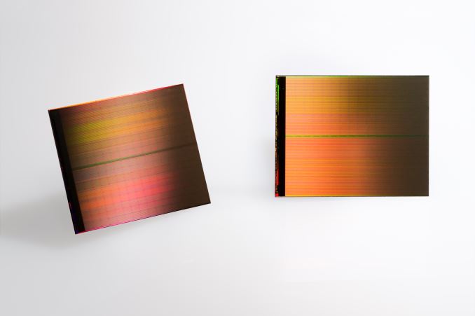
The current mainstream memory technologies, namely DRAM (quick memory accessed by the processor) and NAND (solid-state storage), have been around for decades. While the cell designs have evolved over the years to allow scaling to 20nm and below, the fundamental physics behind DRAM and NAND operation haven't changed a bit and both technologies have their unique technological limitations. DRAM offers nanosecond-level latency and unlimited endurance, but this comes at the cost of large cell size, cell volatility, and power consumption. Since DRAM cells need to be constantly refreshed, the cells don't retain data in an off state, requiring quite a bit of power and making DRAM unsuitable for permanent storage. NAND, on the other hand, has much higher latency (especially write operations) and has a limited number of write cycles, but the cells are non-volatile and the structure is much more efficient, enabling low cost and suitability for storage.
Combining DRAM and NAND at the system-level architecture provides the best of both worlds, which is why modern computers use DRAM as a memory/cache and NAND for storage. However, there's still a latency and capacity gap between DRAM and NAND, so the question arises: what if you were to combine the best of DRAM and NAND at the silicon level? The mission of next generation memory technology across the industry has been to develop a new type of memory that provides low latency and high endurance while offering a small and scalable cell size.
We have seen numerous startups, such as Crossbar and Nantero, discuss and demonstrate their next generation memory technologies, but we have yet to see the established DRAM and NAND vendors come out with their solutions. Intel and Micron are here to change that with the announcement of their new 3D XPoint (Cross Point) non-volatile memory technology this week.
First and foremost, Intel and Micron are making it clear that they are not positioning 3D XPoint as a replacement technology for either NAND or DRAM, and in that scale it has been talked about more in its applications nearer NAND than DRAM. It's supposed to complement both and provide a technology that sits in between the two by filling the latency and cost gap exists between DRAM and NAND. Basically, 3D XPoint is a new tier in the computer architecture because it can be used as either slower, non-volitile memory or much faster storage.
| DRAM | 3D XPoint | NAND | |
| Endurance (P/E Cycles) | 10^15 | 10^7 | 10^3 |
| Read Latency | Nanoseconds | 10s of Nanoseconds | ~100 Microseconds |
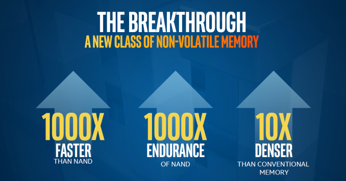
Intel and Micron are claiming that 3D XPoint provides up to a thousand times higher endurance than NAND. Assuming that the numbers are relative to modern (15-20nm) MLC NAND, the endurance should be in the order of a few million P/E cycles; though the marketing materials are claiming up to tens of millions of write cycles. If we assume 3 million write cycles (1000x of what modern MLC has), a 256GB 3D XPoint based drive would have a total write endurance of 768 petabytes. That's equivalent to 420TB per day for five years, or 4.9GB per second. For storage applications that currently rely on NAND, 3D XPoint will eliminate any potential endurance concerns, but it's not durable enough to challenge DRAM in that front since DRAM endurance is essentially infinite. Whether 3D XPoint provides enough endurance to replace DRAM ultimately depends on the application, but especially in certain enterprise workloads there's a need for DRAM.
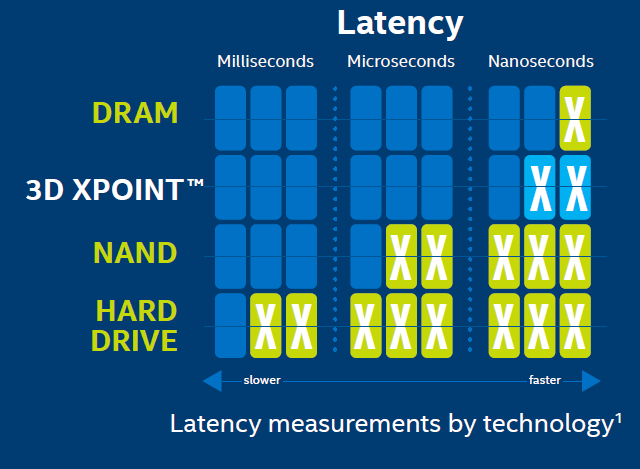
3D XPoint latency should be in the order of 10s of nanoseconds, but the companies didn't specify whether this is read or write latency. Judging by the graphs provided by Intel, it seems to be read latency because NAND write latency would measured in milliseconds (typically 1-2ms for a full page write), whereas the graph puts NAND latency at tens of microseconds that is in line with NAND read latency. Write latency is likely higher than that, probably at least 100s of nanoseconds or even a few microseconds given Intel and Micron's claims of "up to 1000x faster than NAND", but what complicates things is that 3D XPoint is accessible at the bit-level whereas NAND is page-level, so comparing the latency of the two without extended context is quite difficult. In any case, 3D XPoint performance should be closer to DRAM than NAND, but since Intel and Micron aren't discussing any specific latencies yet it's too early to make any final conclusions.
Meanwhile unlike many next generation memory technologies out there at the moment, 3D XPoint is the furthest along and doesn't only exist on paper or in a lab. Intel and Micron are currently sampling the first generation die that is being produced at the companies' jointly owned fab in Lehi, Utah. The die is 128Gbit (16GB) in capacity, whereas the products that startup memory companies have in production are in the order of dozens of megabytes. The die is built on a 20nm node and consists of two layers, and in the future scaling will happen through both lithography shrinks and by increasing the number of layers.
The Utah fab has been producing 20nm NAND for now since Intel didn't invest on the 16nm shrink and all initial 3D NAND production will take place in Micron's Singapore fab, but it's unclear whether the full fab with its 20,000 wafers per month capacity will be dedicated to 3D XPoint from now on. My guess would be that 3D XPoint will gradually take over the full wafer capacity in Utah depending on how the market reacts to the new technology and how high demand Intel and Micron are seeing. 3D XPoint does require some new equipment for manufacturing since 3D XPoint deals with a whole new set of materials, but Intel and Micron said that the transition is quite similar to a new NAND node and allows some of the existing equipment to be used.
The companies aren't quoting any price per gigabyte yet, but since the whole function of 3D XPoint is to fill the gap between DRAM and NAND, it will also be priced accordingly. A quick look at NewEgg puts DRAM pricing at approximately $5-6 per gigabyte, whereas the high-end enterprise SSDs are in the range of $2-3. While client SSDs can be had for as low as $0.35, they aren't really a fair comparison because at least initially 3D XPoint will be aimed for enterprise applications. My educated guess is that the first 3D XPoint based products will be priced at about $4 per gigabyte, possibly even slightly lower depending on how DRAM and NAND pricess fall within a year.
The Technology: How Does 3D XPoint Work?
The way 3D XPoint works is fundamentally very different from NAND. Whereas NAND defines bit values by trapping a varying number of electrons in an insulated floating gate, 3D XPoint is a resistance based technology that works by a bulk property change to alter the resistance level of a cell and thus differentiate between a 0 and 1.
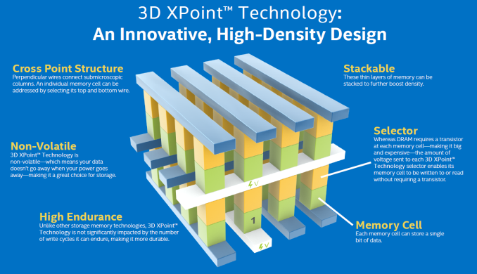
The 3D XPoint structure is very simple. It consists of a selector and memory cell, which sit in between a wordline and bitline (hence the "crosspoint" name). Applying a specific voltage on the wordline and bitline will activate a single selector and enables the cell underneath to be either written (i.e. a bulk property change in the memory cell material) or read (allows the current through to check whether the memory cell is in high or low resistance state). I suspect that write operations require a higher voltage than read because otherwise there might be a risk of triggering a bulk material change (i.e. write operation) while reading a cell. Intel and Micron wouldn't disclose any internal read/write voltages, but we were told that the voltages are considerably lower than in NAND, which requires ~20V for program/erase to create an electric field strong enough to tunnel electrons through an insulator. The lower voltages should, in turn, result in lower power consumption compared to DRAM and NAND.
As the name suggests, the cells can be stacked in a 3D fashion to further improve density and the first generation die that is currently sampling a a two-layer design. Two layers does sound few compared to 3D NAND that is already at 32 layers with 48 being close to production, but the way 3D XPoint array is built is fundamentally quite different.
3D NAND is manufactured by first depositing alternating layers of conducting and insulating materials on top of each other. It's only after all layers have been deposited that the "cell towers" are lithographically defined, followed by a high aspect ratio etch with the hole being filled by channel material to gain access to a memory cell in each layer. In 3D XPoint, however, each layer needs to be lithographically patterned and etched (i.e. repeating the same process for each layer) before another layer can be deposited, which does take away some of the economic benefits that 3D NAND has (i.e. very few lithography steps), but the 3D XPoint approach still provides higher density than what pure lithography based scaling would.
Intel and Micron said that scaling in future will happen through both lithography and 3D stacking of layers. Being scalable both horizontally and vertically is the key in enabling future-proof scalability because traditional Argon Fluoride based immersion lithography with multi-patterning is getting quite uneconomical at ~10nm and there is still no clear successor in the pipeline. The big bets seem to be on EUV and Intel-Micron confirmed that 3D XPoint will (unsurprisingly) be compatible with EUV lithography and the cell design can scale down to single digit nanometers without major impact on endurance/reliability (in fact, some aspects actually get better as the lithography is scaled down), but we are still at least a few years away from EUV being ready for use in high volume mass production. Initial EUV production will also focus on logic given the high equipment cost and because logic cannot be scaled vertically as easily as memory can due to heat issues.
In theory, 3D XPoint also supports multiple bits per cell, but that's not a path Intel and Micron are pursuing at the moment. While it's relatively easy to demonstrate multiple resistance levels in a lab, it's far more difficult to produce tens of thousands of wafers with each die having the necessary characteristics for proper multi-level cell operation. For comparison, it took nearly two decades before a second bit per cell was introduced to NAND, so for now Intel and Micron will focus on lithography and 3D scaling to increase density and cost efficiency, but multi-level cells may become a viable alternative in the future.
One of the big architectural differences to NAND is the fact that 3D XPoint is accessible at the bit-level. In NAND a whole page (16KB for the latest nodes) had to be programmed at once in order to save just one bit of data and to make matters worse you could only erase at the block level (a couple hundred pages at least). As a result, NAND requires sophisticated garbage collection algorithms for efficient performance, but regardless of the level of sophistication there is still performance degradation as a drive enters steady-state because of the inherent read-modify-write cycle that is needed to erase invalid pages within a block. With each cell being individually accessed 3D XPoint doesn’t necessarily require any garbage collection to work effectively, which simplifies the controller and firmware architecture, and even more importantly enables higher performance and lower power consumption.
I suspect that end products, especially storage focused, may still employ logical pages to reduce the tracking overhead because tracking data at a bit level would require a massive cache. However, Intel and Micron made it clear that today’s announcement was solely a technology announcement, so the companies declined to comment anything about upcoming products based on the new technology. That said, both are working on their own products with first commercial shipments scheduled for next year.
The Memory Cell: What's the Secret Behind 3D XPoint?
Section by Ian Cutress
At an array level, 3D XPoint operation is rather easy to understand, but what happens inside the memory cell during a bulk property change is a more complex issue. Personally, what comes to mind is that there are two ways in order to do this – physically adjust the properties of the cell with an external stimulus that adjusts the crystal structure, or chemically adjust the properties of the material used in the cell. During the discussions after the announcement, we were told categorically that this is not a phase change material, eliminating one potential avenue that it might be the change in the crystal structure of the cell producing the resistance change. This also makes a lot of sense, given the claims of a high durability where a constant crystal structure change could have affected the metal bonding between different parts of the cell as inter-structure atom lengths adjusting frequently. This leaves a chemical adjustment, or specifically the realignment in the electron structure of the bit in the cell, that promotes the resistance difference.
After some research, it’s worth talking about the types of technologies that could be being used here.
Spin-Crossover
From previous experience, my fingers automatically point to spintronics and the application of spin-crossover compounds. The short version of this means that a material can have two different resistance levels depending where exactly the electrons are in the electron levels of the structure, and an external stimulus (temperature, high voltage, magnetic field) can be used to switch between the two.
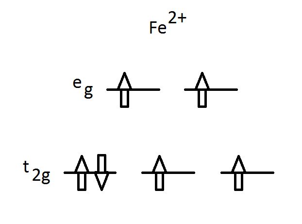
For the long answer, it is best to consider individual transition metal atoms. Depending on the local arrangement around the metal, the bonding orbitals of the metal are partially filled with electrons:
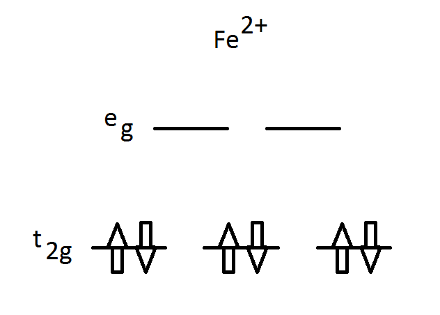
Here is an iron molecule in a 2+ environment, with its main bonding orbitals called t2g (lower energy) and eg (higher energy). Due to Pauli’s exclusion principle, each of the six electrons are paired into three orbitals and each pair of electrons has one ‘spin-up’ and one ‘spin-down’. This is the ground state, also known as the low-spin state as the total spin, S, is equal to zero, as each electron of spin 1/2 is cancelled out by the other electron having -1/2.
The other mode for this atom is the high-spin state where two electrons move to the higher bonding orbitals giving a total spin of S = 2:
Due to an external stimulus, two of the electrons have flipped their spin and occupied the higher energy eg orbitals and this is officially a ‘metastable’ state. Depending the arrangement around the atom, this state could fundamentally be very stable and yet have wildly differing properties to the original ground state.
Extrapolating this out into a bulk material is fundamentally difficult. A quick look at research papers suggests that spin-crossover compounds can be directly applied between junctions and their resistance changed, but the chemical base for such operations in many papers are carbon nanotubes, graphene layers or organic chains.
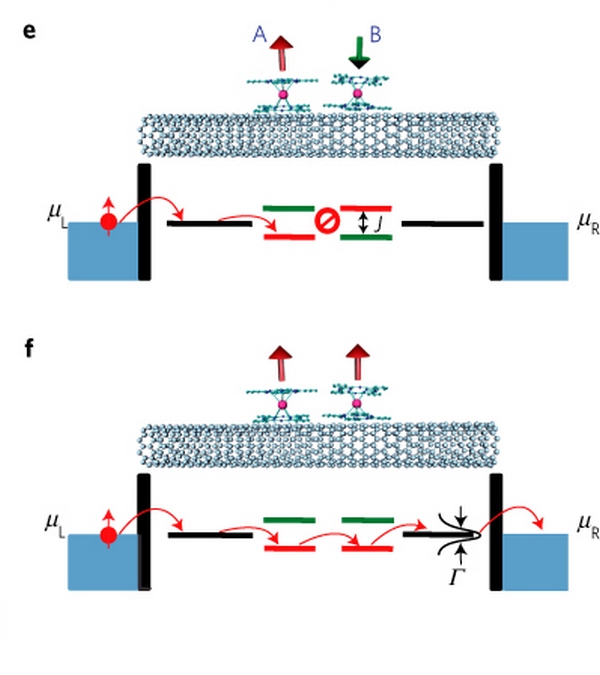
Image from M. Urdampilleta et al., Nature Materials, 10, 502 (2011)
In this paper, the orientation of the low-spin/high-spin states either affords conductivity between the two edges or does not, and depending on the metal in question will determine the exact nature, resistance, characteristics and/or stability of the platform. Intel will have had to have developed a material that is essentially programmed by voltage rather than any other stimulus, which adds to the complexity. Normally spin-crossover compounds have a specific temperature window as well which has a direct impact on stability as electrons may migrate from the high-state to low-state.
At this point, the scalability and fundamental material characteristics are the major barriers to large scale output of spin-crossover, particularly if nanotubes are required. If it was somehow extended to bulk metallic materials, as you bring an individual metal environment to bulk, band lines (and gaps) start to blur between simple orbital theories, so how it can be incorporated it into a cell is unknown. Intel is also stating that their technology is capable of multiple bits per cell, and the reality of spin-crossover arrangements can be blurred with electron tunnelling to achieve that effect.
Spin-Transfer Torque
The STT method of memory cells relies on both the resistance between the states of the cell, as well as the ability to control magnetic fields within a cell itself. The short version is that if you adjust the magnetic alignment of a material, you can adjust the resistance and use it as a form of memory.
The long form for STT relies on a feature known as spin-polarised current. Electrons intrinsically have spin in two directions, up or down, and electric current typically consists of an even mix of these two, giving an overall un-polarised current (i.e. no overall spin direction majority). When an unpolarized current is passed through a thick layer of magnetic material, it causes the current to become polarised. If this polarised current then passes through a thin magnetic layer with a different density of electron states, the polarization of the current can cause the magnet to flip due to more electrons relaxing into states of opposite spin.
With the thick layer having a constant magnetic orientation and the thin layer (or the free layer) being able to flip, depending on the material, the resistance between the two combinations can act as a memory cell.
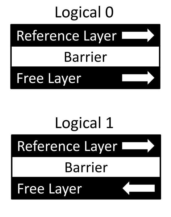
From Evaluating STT-RAM as an Energy-Efficient Main Memory Alternative, Kültürsay et. al.
Claimed benefits from STT methodologies revolve around energy consumption with it being lower to DRAM but with equivalent performance. Barriers to the technology depend on the ability to essentially create permanent magnets at such a small nanolithography note, and how placing many small magnets near each other (similar to bits on a HDD) might cause some of them to flip unexpectedly. Also with this method, it is unclear if it can scale beyond a simple binary bit per cell, and available research suggests that it requires a control transistor, which Intel has stated that 3D XPoint does not use.
Public history of STT development comes from a 1-megabit IC from Qualcomm on 45nm in 2011, and a 64-megabit module from Everspin in 2012 although no mention of a node.
Conductive Bridging
One of the easiest ways to adjust the resistance of a pathway is to block the path of electrons almost completely with a physical change. Conductive bridging technologies (or programmable metallization cells) rely on the creation of a nano-bridge between electrodes to reduce the resistance of a cell using a similar technique to electrolysis.
Within a CB cell, a thin film of electrolyte (historically a liquid, but can be a solid) is sat between an active and an inert electrode. When a negative bias is applied to the inert electrode the metal ions in the electrolyte are reduced to form metal atoms. When enough of these metal atoms are reduced and connected, it forms a wire between the two electrodes. In order to break the wire, the reverse potential difference is applied and the atoms in the wire are oxidized to become part of the electrolyte again. Ultimately the electrode-electrolyte-electrode combination is still conductive, but its resistance is higher than that of the situation where a wire is created.
Even discussing a brief overview of CB, for anyone familiar with electrolysis, brings up a large number of questions. First might be the use of liquids in a cell, but we should assume here that we might be dealing with mobile ions in a solid moving between intercalation points (spaces between a lattice/framework) anyway. But for me it comes to the growth of this ‘wire’. Typically growth via electrolysis is somewhat undirected – you are relying on the activity of various crystal planes to drive growth and ion diffusion is multi-directional, though there will be a slight bias towards the electrode depending on the crystal plane of growth. That leads to forked wires, similar to the way lightning works. When you do make a connection between the electrodes, or at least within electron tunneling distance, the resistance differential with the wire (from high resistance to low resistance) is large, but as the wire grows it will again decrease the resistance. This makes the wire method potentially multi-bit per cell, but as I mentioned before, growth control is hideously difficult. The other factor is that of reversing the process – typically the active electrode is made from the same material as the ions, meaning that the electrode itself could essentially dissolve. This creates a few headaches in research at least for durability.
To the benefit of CB, it theoretically scales to smaller than floating gate cells and the layout is simpler, with reported benefits in both power and performance by several orders of magnitude over current NAND.
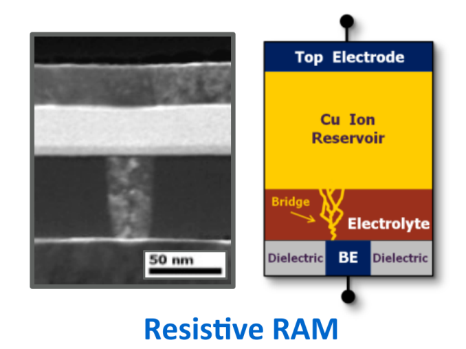
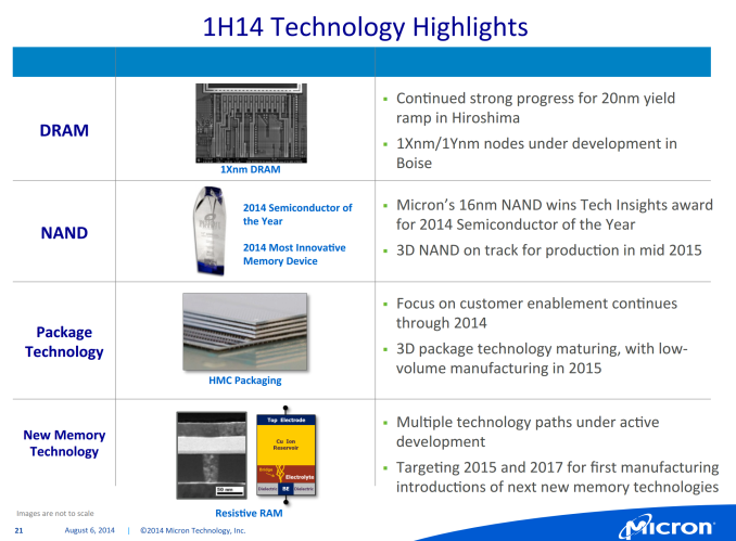
Despite these issues and benefits, I might suggest that CB is currently the leading contender for the technology used in 3D XPoint. Subtle hints such as the official licensing of the technology by Micron in 2002, but also this slide in Micron’s Analyst conference in 2014 shows how they’ve overcome some of the issues I’ve listed above:
At the bottom here is the image above of a working cell along with a diagram showing how the bridging works. In order to facilitate the active electrode not being ‘eaten’ in reverse programming, we have a large ion reservoir to call on. The other electrode is also small in order to direct wire growth. As long as the electrolyte layer is small (several monolayers), read/write speeds can be quick and easy.
The Future
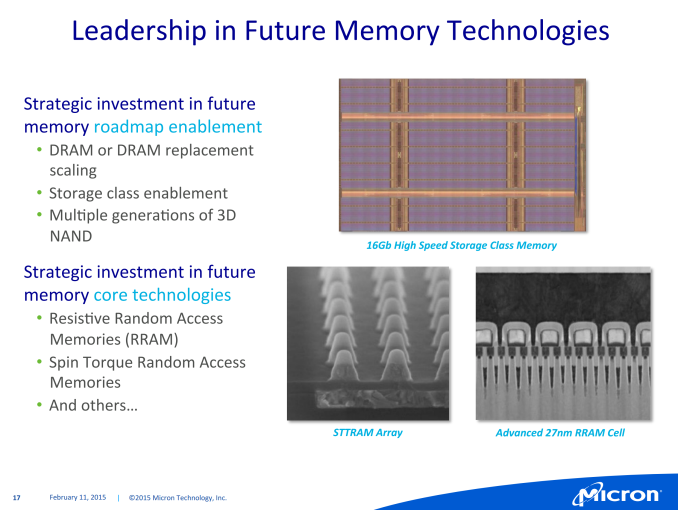
With all that being said, if we fast forward to Feb 2015, Micron released this slide at an analyst meeting:
In the bottom half of this slide, it’s clear that Micron is looking into spin-transfer torque based memory on the left, and several analyst reports has suggested that the RRAM cell on the right is most likely that of CB technology. Within the 3D XPoint slides presented at the announcement this week, a number of analysts have also concluded that the selector per bit is most likely a diode in order to enable the appropriate characteristics for probing the resistance.
Given the fact that the announcement has stated that what is being done here is fundamentally different to previous attempts, and that the hardest part of producing 3D XPoint is the materials, I ultimately can’t judge on the exact specifics of what Intel and Micron are doing here, only that the conductive bridging method is most likely the method by which it is being done. Chances are the exact details will be kept close to Micron and Intel’s chest for a while as they are quoting a full decade research time from concept to product, which aligns from the 2002 licensing deal mentioned above for the conductive bridging method.
Estimating 3D XPoint Die Size
By now most of you probably know that I'm a sucker for die sizes and since this is information that the DRAM and NAND vendors are unwilling to share, I've gone as far as developing my own method for estimating the die size (well, it's really just primary school geometry, so I can't take too much credit for it). Die size is the key factor in determining cost efficiency because it directly relates to the number of gigabytes each wafer yields and thus it's a vital metric for comparing different technologies and process nodes.
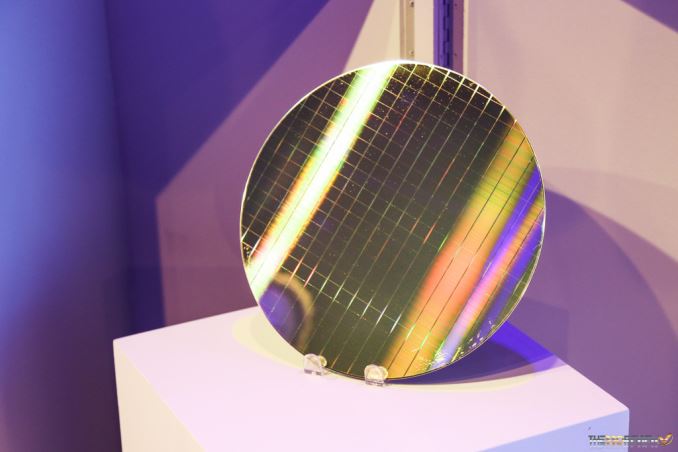
I'm borrowing the above picture from The SSD Review because to be honest my wafer photos (and photos in general) are quite horrible and wafers are far from being the easiest object given all the reflections. Sean is a professional photographer, so he managed to grab this clear and beautiful photo of the production 3D XPoint wafer Intel and Micron had on display, making it easy to estimate the die size.
I calculated 18 dies horizontally and 22 vertically, which yields 227mm^2 with a normal 300mm wafer. When taking die cuts (i.e. the space between dies) into account, we should be looking at 210-220mm^2. Array efficiency is about 90%, which is much higher than planar NAND because most of the peripheral circuitry lies underneath the memory array.
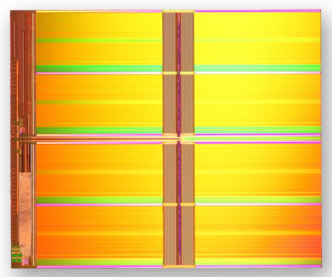
IMFT 20nm 128Gbit MLC NAND die
For comparison, Intel-Micron's 20nm 128Gbit MLC NAND die measures 202mm^2 and has array efficiency of ~75%. From that we can calculate that the 128Gbit memory array in 3D XPoint takes about 190mm^2, while a similar capacity planar NAND array measures ~150mm^2 (since the 128Gbit 3D XPoint die consists of two layers and 128Gbit MLC NAND die stores two bits per cell, the number of layers and bits stored per cell cancel out). It seems like NAND is denser (about 20-25%) from a memory array perspective given a fixed feature size (i.e. lithography), but at this point it's hard to say whether this is due to the cell design itself or something else. Connecting layers of wordlines and bitlines to the intermetal layers likely takes some extra area compared to a 2D process (at least this is the case with 3D NAND), which might partially explain the lower density compared to NAND.
However we will have to wait for some SEM photos to really see what's happening inside the 3D XPoint array and how it compares to NAND in cell size and overall density efficiency. Of course, there is a lot more in total manufacturing cost than just the cell and die size, but I'll leave the full analysis to those with the proper equipment and deeper knowledge of semiconductor manufacturing processes.
What Happens to 3D NAND
The above analysis already gives a hint that 3D XPoint isn't about to replace 3D NAND, at least not in the foreseeable future. That's also what Intel and Micron clearly stated when asked about 3D XPoint's impact on 3D NAND because it's really a new class of memory that fills a niche that DRAM and NAND cannot. The companies are still looking forward to rolling out 3D NAND next year and have a strong roadmap of future 3D NAND generations.
As I mentioned earlier, the way 3D XPoint array is built is quite different from 3D NAND and my understanding is that it's less economical, which is one of the reasons why the first generation product is a two-layer design at 20nm rather than dozens of layers at a larger lithography with single patterning like 3D NAND is. Unless there's a way to build 3D XPoint arrays more like 3D NAND (i.e. pattern and etch multiple layers at the same time), I don't see 3D XPoint becoming cost competitive with 3D NAND anytime soon, but then again it's not aimed to be a NAND successor in short-term.
What happens in ten year's time is a different question, though. 3D NAND does have some inherent scaling obstacles with vanishing string current likely being the biggest and most well known at this point. Basically, the channel in each 3D NAND "cell tower" (i.e. a stack of layers, currently 32 for Samsung and Intel-Micron) is a single string that the electrons have to flow through to reach every individual cell in the string. The problem is that as the length of the string increases (i.e. more layers are added), it becomes harder to reach the top cells because the cells on the way cause disturbance, reducing the overall string current (hence the name "vanishing string current"). For those who are interested in a more detailed explanation of this issue along with some experimental data, I suggest you head over to 3D Incites and read Andrew Walker's post on the topic.
Since most vendors haven't even started 3D NAND mass production, it's not like the technology is going to hit a wall anytime soon and e.g. Toshiba-SanDisk's 15nm NAND has strings consisting of 128 cells, but like any semiconductor technology 3D NAND will reach a scaling limit at some point. Whether that is in five, ten or twenty years is unknown, but having a mature and scalable technology like what 3D XPoint should be at that point is important.
Products
During the event, Intel and Micron made it clear that this week's announcement is solely about the underlying 3D XPoint technology. Products based on this new technology will follow sometime next year and the companies were quite tight-lipped when it came to details, but they did give away a few hints. First of all, the co-operation between Intel and Micron only exists at the memory technology level and both companies are developing their own 3D XPoint based products, similar to how the two have operated in the SSD/NAND business. Technically this means that the two will be competing against each other, although it's possible that each company will take a unique approach to utilizing 3D XPoint in an end product.
One take away from the presentation and Q&A was Intel's emphasis on NVMe. Intel has been a strong advocate of the technology ever since its inception, and as a matter of fact Intel was the first SSD vendor to ship NVMe SSDs in high volume with the introduction of the DC P3700 and its derivatives last year. While NVMe has mostly been associated with NAND so far since it is mainstream non-volatile memory, the core architecture was built to scale with future memory technologies with even lower latencies (after all, NVMe stands for Non-Volatile Memory Express). Given that software interfaces tend to stick around for at least a decade, it's obvious that NVMe had to be designed with more than just NAND in mind.
With NVMe it's certain that we will see 3D XPoint based PCIe SSDs. Whether these will be add-in cards or 2.5" drives remains to be seen, but I'm more inclined to say add-in cards (at least initially) because of the connector limitations. U.2 (former SFF-8639) supports only four PCIe 3.0 lanes, resulting in effective real world bandwidth of about 3.2GB/s. NAND is already capable of saturating that for read operations, so even though 3D XPoint would improve write and random IO performance, the full potential would ultimately go unused without a higher bandwidth interface. An add-in card doesn't share the limitations of U.2 and could support up to 16 lanes with over 10GB/s of bandwidth available, but the downside would more limited serviceability since add-in cards can't be front-loaded like 2.5" drives can. As the enterprises have used add-in cards in the past (Fusion-io never made anything but add-in cards), I don't see serviceability being a major hurdle for the companies that really need 3D XPoint for their workloads. On the other hand, I wouldn't be surprised to see Intel pushing for an 8-lane U.2-like standard, but it really needs industry-wide support to get air under the wings.
With Intel being the other party in the joint-venture, it's guaranteed that 3D XPoint will get all support and love it needs on the platform side. Intel can integrate more PCIe lanes and/or accelerate the development of PCIe 4.0 for its upcoming platforms to create the necessary bandwidth and push for 3D XPoint if needed, which is something that no other memory vendor could do.

AgigA's DDR4 NVDIMM: A Future 3D XPoint Form Factor?
While Intel will clearly be pursuing the storage aspect of 3D XPoint through NVMe, I suspect Micron might take a more memory-like approach since it's a memory company as much as it's a storage company. It was made clear that 3D XPoint can be used in memory and storage applications because the technology is bit-addressible and can work in a similar fashion as DRAM. Bringing 3D XPoint closer to the CPU and connecting it through a DDR4 interface would obviously yield the best performance and eliminate any bottlenecks that PCIe has. There are already NAND-based products that do this, such as SanDisk's ULLtraDIMM, and a couple of months ago JEDEC paved the way by releasing a standard for DDR4 NVDIMMs, a new standard set to fill the gap between DRAM and SSDs. While NVDIMMs will require driver work due to the lack of standardized software interface like NVMe, I do believe 3D XPoint is the right technology for bringing NVDIMMs to the market and it would make sense for Micron to do so.
Applications
Section by Ryan Smith
The use cases for 3D XPoint are potentially significant in number and Intel/Micron believe that it will open the doors for all sorts of new applications. Overall the computing industry has had access to high speed non-volatile memory technologies before – magnetic core memory is the traditional poster child here – so there is some precedence here and some fundamental research into the field from the early days of computing. However with magnetic core memory having become outmoded before the majority of our readers were even born, the modern computing industry has developed around the current paradigm of fast DRAM and slow permanent storage. As a result while the potential applications are numerous, it’s still in many ways an uncharted area in computer science.
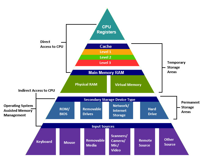
The most immediate application of 3D XPoint based products will be as a layer of storage between DRAM and SSDs. Over the history of computing the number of layers between storage and processors has continued to build – multiple layers of on-die caches, off-die caches, caching SSDs, etc – and 3D XPoint memory would further fit into that heiarchy as a storage medium that bridges the gap between DRAM and the current fastest non-volatile storage. By treating 3D XPoint memory as another layer of cache, 3D XPoint can be used to further speed up applications that are currently bound by either memory capacity or storage latency.
 <
<
The Traditional Memory Heiarchy (Image Source: Tommy MacWilliam, Harvard)
Given the costs of 3D XPoint, the first such applications are expected to be on the enterprise side. Enterprise users make heavy use of storage at all layers in order to balance performance needs against the relatively small capacity of DRAM. Database servers in particular adapt well to caching, and it’s easy enough to imagine a next-generation database system using 3D XPoint to backstop DRAM. Since 3D XPoint is non-volatile, it can even be an exclusive cache – that is, its contents don’t need to be in lower layers as well – which eliminates a good deal of overhead. A database system in this context would only need to write contents to SSDs and other, lower layers of storage when data gets expelled from the 3D XPoint cache, an occurrence that may be particularly rare with the properly tuned database.
Many of these benefits of a cache layer are applicable to other types of storage-heavy servers as well, though I expect databases will be the king. Perhaps the more interesting aspect – and certainly more relatable to the public at large – will be what 3D XPoint-backed servers are used for. Intel and Micron are eager to point out the “big science” uses for the technology; projects and systems such as the Large Hadron Collider and Oak Ridge’s Titan supercomputer can generate a massive amount of data, and while processing all of that data is first and foremost a processor issue, feeding that data for processing is a big problem as well. Any kind of analysis that could benefit from individual processors having RAM-like access to an SSD-sized pool of data could benefit.
The catch is that there’s still a lot of research that’s needed into figuring out what the best uses may be. This kind of shift in access times and capacity doesn’t just make computers faster, but it can change the fundamentals of what algorithms are best. Just as how GPUs required scientists to figure out how to spread out their work in a massively parallel (and high latency) nature, putting 3D XPoint to its full use will require newer algorithms that are capable of effectively utilizing direct access to so much data at once.
Meanwhile I would be surprised if the financial industry didn’t jump on this early, as they are prone to jumping on major technologies in order to try to get an edge in a highly competitive and lucrative field. In this aspect it’s not so much that 3D XPoint would improve processing speed – such work is already offloaded to large RAM pools when possible – but rather it would enable traders and analysts to run simulations against much larger datasets much more effectively.
As for the consumer space, the same principles about an additional cache layer would apply, but I’m not so sure we’d see consumers pick it up in the same manner. Much of this has to do with what the eventual costs and capacities of 3D XPoint products would be, as consumers are much more price sensitive than professional users. In the consumer space we’ve seen sporadic use of NAND-backed hard drives, for example, but by and large consumers have stuck with discrete SSDs and HDDs. Consumers either don’t want to pay the premium for SSDs, or have enough money to just buy large SSDs outright, leaving little of a middle ground.
That said I’ve seen some interesting pitches for 3D XPoint in the gaming space that have some merit, as games are something of a special case for consumer workloads. By and large we want fast access to game resources since those resources are accessed on-demand and are needed to progress in a game’s execution, but the assets themselves aren’t volatile. Only a small part of the working set for a game is volatile data – player positions, AI decision trees, game state, etc – while the rest of it is static data such as models, world geometry, and textures. 3D XPoint in turn would be fast enough that it could be used as a replacement for RAM in holding these assets, but as the data is non-volatile it wouldn’t thrash 3D XPoint P/E cycles very much, and any write speed disadvantage compared to DRAM would be immaterial.
But again, this is going to depend on the cost of the technology; if it were to become cheap enough that 50-100GB could be thrown in a game console or gaming PC, then you could store the entirety of most games in 3D XPoint memory, which would reduce load times to the time required to process the data and setup the game state. This is more important in consoles which currently store their games on a mechanical drive, who then could recall data rather quickly on first boot or adjust for large amounts of memory swapping for more detailed titles. High end PCs with large amounds of DRAM can already use RAMDisks perhaps nullifying a point there.
Last but not least of course are the implications for 3D XPoint as a wholesale replacement for DRAM. The more limited lifetime of 3D XPoint relative to DRAM certainly poses some challenges in this respect, but I suspect the bigger issue will be overall bandwidth. By the time 3D XPoint becomes available in bulk, DRAM technology should be to the point where faster-generations of DDR4 are available and HBM is widely deployed. Given that future generations of HBM are targeting 1TB/sec or more of memory bandwidth, it’s unlikely that 3D XPoint is going to be able to match the bandwidth of contemporary high-bandwidth DRAM solutions. So any rumors of the impending death of DRAM are likely premature.
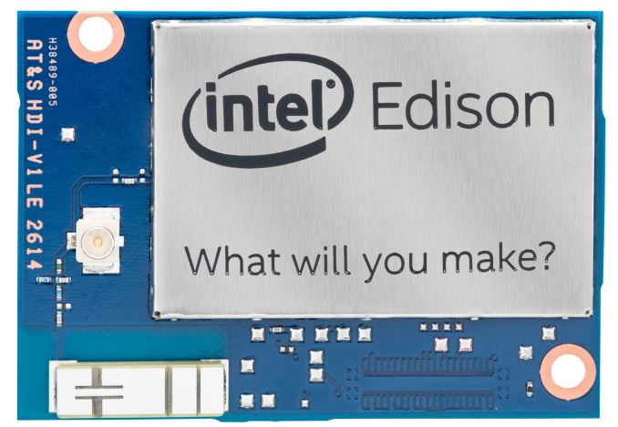
IoT & Embedded, A Good Fit For 3D XPoint?
But with that said, while 3D XPoint isn’t likely to replace DRAM in a wholesale manner for all applications, there is clearly room for it to replace DRAM in some situations where DRAM is used primarily for its bandwidth and latency versus solid state storage. Replacing DRAM with 3D XPoint in embedded applications for example would be very practical – many embedded uses don’t need high bandwidth or low latency as much as they just something better than traditional NAND – and I wouldn’t rule out smartphones here either, at least to an extent. If individual 3D XPoint chips can be produced small and cheap enough, then the most lucrative use for the tech as a DRAM replacement may be in the vast legions of low-performance devices, rather than in high-performance hardware that actually needs the full speed and latency of DRAM.
Final Thoughts
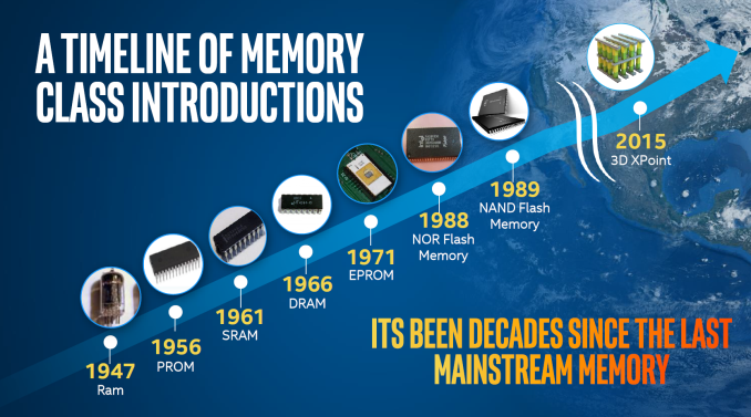
3D XPoint has a lot to chew on. There hasn't been an announcement this big in the memory industry since the invention of NAND in 1989 and while DRAM and NAND have improved and scaled a lot over the decades, 3D XPoint is really a new class of memory. It's fast, durable, scalable and non-volatile, whereas DRAM and NAND each only meet two of these criteria. It fills the niche between DRAM and NAND by taking the best characteristics of both technologies and creating a memory unlike anything we have seen before.
The significance of the announcement isn't just the new memory technology, but that it's actually in production with volume shipments scheduled for next year. Intel and Micron have succeeded in bringing a concept from a lab to an actual fab, which is by far the most difficult part in any new semiconductor technology. Something that works well in a lab may not be mass producible at all, but Intel and Micron made the necessary investments to develop new material compounds and surrounding technologies to turn 3D XPoint into a real product. It will be interesting to see how the other DRAM and NAND vendors respond because the memory industry is one where you don't want your rivals to have something you don't for an extended period of time.
However, it's clear that 3D XPoint isn't a true DRAM or NAND successor and Intel and Micron aren't trying to position it as such. DRAM will still have its market in high performance applications that require the latency and endurance that 3D XPoint can't offer. Our early cost analysis also suggests that 3D XPoint isn't as dense as planar NAND, let alone 3D NAND, but by having the ability to scale both vertically and horizontally 3D XPoint may have the potential to replace 3D NAND in the long run.
Looking further into the future, 3D XPoint isn't the only technology Intel and Micron are cooking. If the two stay on schedule, we should be hearing about their other new memory technology in roughly two years. As 3D XPoint seems to be more suitable as a 3D NAND replacement, the second new technology might be one that is capable of taking DRAM's place in the long run.
All in all, it's impossible to think of all the possible applications that 3D XPoint will have in the future because it's a technology that hasn't existed before. I don't think it's an overstatement to say that 3D XPoint has the potential to change modern computer architectures and the way we see computing, but that transition won't happen overnight and will likely require competing technologies from other vendors to fulfill the demand. What is clear, though, is that Intel and Micron are leading us to a new era of memory and computing next year.

