Original Link: https://www.anandtech.com/show/941
GPU Shootout with Unreal Tournament 2003 Part II: CPU Scaling
by Anand Lal Shimpi on July 9, 2002 9:48 AM EST- Posted in
- GPUs
One week ago we put a total of 19 different GPUs through the toughest tests they’ve encountered in our labs: non-stop benchmarking using Unreal Tournament 2003. Using a couple of levels of UT2003 we were able to get an idea for the performance levels these GPUs would enjoy when the forthcoming game is released.
In order to save time we conducted that comparison entirely on one platform, an Athlon XP 2100+ on an EPoX KT333 motherboard. When we queried you all about whether you’d like to see CPU scaling tests we received an astounding number of replies asking for just that.
Today we bring you an update to our 19-way GPU shootout with a focus entirely on how these GPUs scale with CPU clock speed.
What are we testing?
The flyby demos Epic provided for us in UT2003 give a good idea of graphics performance but really don’t take into account things like physics and AI calculations, which are inevitably handled by the host CPU.
Instead, these demos measure the speed at which the CPU can provide the GPU with vertex data, which is the first step in the rendering process. The end result is that we’re not taking into account what a faster CPU will be able to do for physics and AI calculations, only how quickly it can feed the GPU the vertex data it needs to run at those high frame rates we desire.
How are we testing?
The first time we introduced our updated CPU scaling methodology was in our Sub-$200 Video Card Roundup, here’s a quick refresher for those of you that don’t remember:
Our goal with these tests was to isolate CPU clock speed as the only variable, not cache sizes, not architectures, not FSB speeds, only clock speed. In order to achieve this we took an Athlon XP 2100+ and unlocked it so that we could adjust the clock multiplier. We kept the FSB set at 133MHz and adjusted the multiplier from 6.0x, yielding an 800MHz clock speed, up to the default 13x multiplier. Although this method produces some unofficial and unavailable processor/FSB/clock speed combinations, it serves our needs perfectly. So although a 800MHz Athlon XP processor running on a 133MHz FSB won’t be directly comparable to a genuine Athlon running at 800MHz, you’ll at least get an idea of what a CPU around that speed would give you, performance-wise.
We stuck to one resolution (800x600) in order to use a low enough resolution to give the slower cards a chance while not making the test entirely CPU-bound. We also ran all of our benchmarks under the DM-Asbestos map, which is entirely indoors and is noticeably less GPU bound than some of the other maps.
Finally, we ran all of the tests at the same two detail settings from our initial roundup: High and Medium. The High Detail settings have every detail option maxed out while the Medium Detail settings disable detailed textures, lower the texture detail level, and lower the model detail level among other image quality/performance tradeoffs. If you haven’t already, be sure to read the original UT2003 performance roundup to get a better feel for the tests we ran.
The test system remained the same from the original comparison.
Specification Comparison: 19 GPUs in a Table
We originally wanted to debut this table in the first article but time constraints kept that from happening so today we bring you a handy table that contains a lot of useful information.
The following table compares the basic specifications of all of the GPUs in this roundup including the GPU’s introduction date (the date we were allowed to publish benchmarks) and the introduction price. It’s always interesting to see how performance specs as well as prices change over time.
| GPU |
Date
Introduced |
Price
when introduced |
Transistor
Count |
Manufacturing
Process |
Core
Clock |
T&L |
Pixel
Pipes |
Texture Units per Pipe |
Memory Size |
Memory Clock |
Memory Bus |
Memory
Bandwidth |
| ATI Radeon 7500 (64MB) | 8/1/2001 |
$200
|
30M |
0.15-micron |
290MHz |
DX7 |
2 |
3 |
64MB |
230MHz |
1x128-bit
DDR |
7.4GB/s |
| ATI Radeon 8500 (128MB) | 2/4/2002 |
$250
|
60M |
0.15-micron |
275MHz |
DX8 |
4 |
2 |
128MB |
275MHz |
1x128-bit
DDR |
8.8GB/s |
| ATI Radeon 8500 (64MB) | 8/1/2001 |
$300
|
60M |
0.15-micron |
275MHz |
DX8 |
4 |
2 |
64MB |
275MHz |
1x128-bit
DDR |
8.8GB/s |
| ATI Radeon 8500LE (128MB) | 2/4/2002 |
$180
|
60M |
0.15-micron |
250MHz |
DX8 |
4 |
2 |
128MB |
250MHz |
1x128-bit
DDR |
8.0GB/s |
| ATI Radeon DDR (64MB) | 7/17/2000 |
$400
|
30M |
0.18-micron |
183MHz |
DX7 |
2 |
3 |
64MB |
183MHz |
1x128-bit
DDR |
5.9GB/s |
| Matrox Parhelia (128MB) | 6/25/2002 |
$399
|
80M |
0.15-micron |
220MHz |
DX8 |
4 |
4 |
128MB |
275MHz |
1x256-bit
DDR |
17.6GB/s |
| NVIDIA GeForce2 MX 200 (32MB) | 4/21/2001 |
$80
|
- |
0.18-micron |
175MHz |
DX7 |
2 |
2 |
32MB |
166MHz |
1x64-bit
SDR |
1.3GB/s |
| NVIDIA GeForce2 MX 400 (64MB) | 4/21/2001 |
$125
|
-
|
0.18-micron |
200MHz |
DX7 |
2 |
2 |
64MB |
166MHz |
1x128-bit
SDR |
2.7GB/s |
| NVIDIA GeForce2 Pro (64MB) | 12/5/2000 |
$300
|
25M |
0.18-micron |
200MHz |
DX7 |
4 |
2 |
64MB |
200MHz |
1x128-bit
DDR |
6.4GB/s |
| NVIDIA GeForce2 Ultra (64MB) | 8/14/2000 |
$500
|
25M |
0.18-micron |
250MHz |
DX7 |
4 |
2 |
64MB |
230MHz |
1x128-bit
DDR |
7.36GB/s |
| NVIDIA GeForce3 (64MB) | 3/22/2001 |
$400
|
57M |
0.15-micron |
200MHz |
DX8 |
4 |
2 |
64MB |
230MHz |
4x32-bit
DDR |
7.36GB/s |
| NVIDIA GeForce3 Ti 200 (64MB) | 10/1/2001 |
$200
|
57M |
0.15-micron |
175MHz |
DX8 |
4 |
2 |
64MB |
200MHz |
4x32-bit
DDR |
6.4GB/s |
| NVIDIA GeForce3 Ti 500 (64MB) | 10/1/2001 |
$375
|
57M |
0.15-micron |
240MHz |
DX8 |
4 |
2 |
64MB |
250MHz |
4x32-bit
DDR |
8.0GB/s |
| NVIDIA GeForce4 MX 440 (64MB) | 2/6/2002 |
$150
|
- |
0.15-micron |
270MHz |
DX7 |
2 |
2 |
64MB |
200MHz |
2x64-bit
DDR |
6.4GB/s |
| NVIDIA GeForce4 MX 460 (64MB) | 2/6/2002 |
$180
|
- |
0.15-micron |
300MHz |
DX7 |
2 |
2 |
64MB |
275MHz |
2x64-bit
DDR |
8.8GB/s |
| NVIDIA GeForce4 Ti 4200 (128MB) | 4/16/2002 |
$200
|
63M |
0.15-micron |
250MHz |
DX8 |
4 |
2 |
128MB |
222MHz |
4x32-bit
DDR |
7.1GB/s |
| NVIDIA GeForce4 Ti 4200 (64MB) | 4/16/2002 |
$180
|
63M |
0.15-micron |
250MHz |
DX8 |
4 |
2 |
64MB |
250MHz |
4x32-bit
DDR |
8.0GB/s |
| NVIDIA GeForce4 Ti 4400 (128MB) | 2/6/2002 |
$300
|
63M |
0.15-micron |
275MHz |
DX8 |
4 |
2 |
128MB |
275MHz |
4x32-bit
DDR |
8.8GB/s |
| NVIDIA GeForce4 Ti 4600 (128MB) | 2/6/2002 |
$400
|
63M |
0.15-micron |
300MHz |
DX8 |
4 |
2 |
128MB |
325MHz |
4x32-bit
DDR |
10.4GB/s |
| ST Micro Kyro II (64MB) | 3/13/2001 |
$150
|
15M |
0.18-micron |
175MHz |
N/A |
2 |
1 |
64MB |
175MHz |
1x128-bit
SDR |
2.8GB/s |
Now let’s get on to the scaling…
NVIDIA’s GeForce4 Line
The following GPUs are featured in the charts below:
GeForce4 Ti 4600
GeForce4 Ti 4400
GeForce4 Ti 4200
GeForce4 MX 460
GeForce4 MX 440
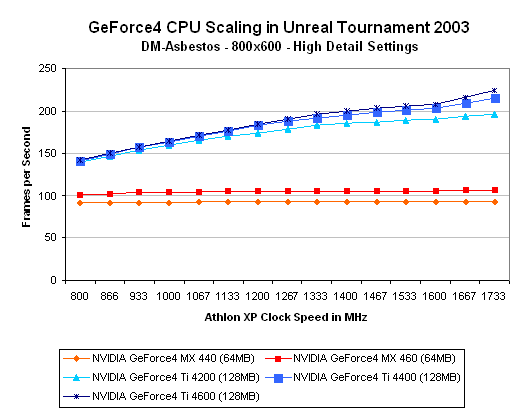
The first thing you’ll notice is that the GeForce4 MX’s curves remain perfectly flat. A faster CPU doesn’t help the performance of the NV17 GPU at all; this puppy is fill-rate limited courtesy of its 2 pixel pipelines. There’s a lot of multipass rendering going on with the GeForce4 MX that guarantees a flat CPU scaling curve.
The true GeForce4 cards exhibit a remarkably different pattern as they demand higher speed CPUs to unlock their potential. With a slow enough CPU you’d be getting more for your money if you went with a GeForce4 MX than a GeForce4.
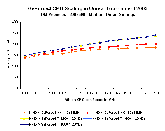
Taking down the detail settings results in the MX cards scaling much more like the GeForce4s.
NVIDIA’s GeForce3 Line
The following GPUs are featured in the charts below:
GeForce3 Ti 500
GeForce3 Ti 200
GeForce3
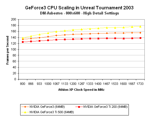
As you’d expect, with relatively slow CPUs the three GeForce3 cards perform very close to one another but the gap grows as clock speed increases. By the time you pass the 1.2GHz mark the GPUs get as far apart from one another as they’re going to get.
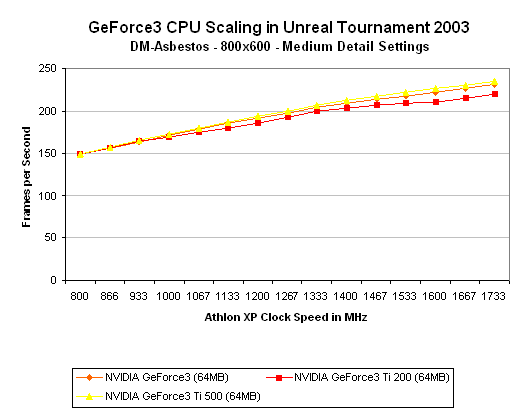
At the Medium Detail settings the CPU scaling curves are all much steeper thanks to decreased dependencies on the GPU’s ability to perform. Running at Medium Detail levels doesn’t make sense for GeForce3 owners but as you’ll see later on, it can definitely help the slower cards.
NVIDIA’s GeForce2 Line
The following GPUs are featured in the charts below:
GeForce2 Ultra
GeForce2 Pro
GeForce2 MX 400
GeForce2 MX 200
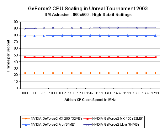
While the GeForce2 Ultra & Pro can definitely pull some high frame rates, the UT2003 benchmark is clearly saturating their abilities as increasing the CPU clock speed by over 116% doesn’t do an ounce of good. At the highest detail settings you’re GPU bound if you have any GeForce2 derivative almost regardless of your CPU speed.
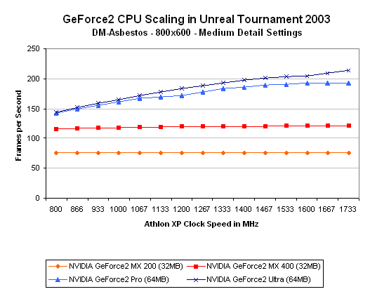
Going down to Medium Detail levels fails to help the GeForce2 MX at all; if you have a GeForce2 MX you had better be looking for a graphics upgrade before you even consider touching that CPU.
The GeForce2 Ultra and Pro scale much better here, but after 1.33GHz the performance benefits start to taper off for both solutions.
ATI’s Radeon Line
The following GPUs are featured in the charts below:
Radeon 8500
Radeon 8500LE
Radeon 7500
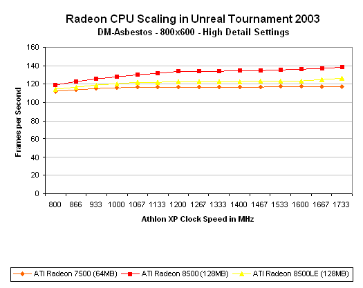
The Radeon 8500 offers GeForce3-class performance under UT2003 and as you can see from the graph above, it scales with CPU speed almost identically.
After 1.2GHz the 8500’s CPU scaling curve pretty much flattens out, and it’s after that point that buying a faster CPU will not result in a tangible increase in GPU performance.
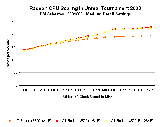
As we drop down to Medium Detail settings you’ll notice that at lower clock speeds (those below 1.2GHz), the Radeon 8500 performs identically to the Radeon 7500. Granted that this doesn’t take into account feature benefits the Radeon 8500 series has over the 7500 but from purely a performance standpoint, Radeon 7500 owners need not think of upgrading their graphics to an 8500 before moving to a faster CPU.
It’s almost immediately once you pass the 1.2GHz mark that the two Radeon 8500 cards can begin to separate themselves from the 7500 by a reasonable margin.
ST Micro’s Kyro II
The Kyro II isn’t a GPU in the same sense that the rest of these solutions have hardware T&L engines, but there’s no point in changing the name of the roundup just to suit it. Because of the lack of a hardware T&L engine the Kyro II is a bit more dependent on a fast CPU since the host CPU’s role extends much further than passing vertex data onto the graphics processor. As the CPU is much more involved in the geometry processing stages a slower processor could limit the GPU at very low clock speeds; finding out approximately what clock speeds those are is what these charts should help us do.
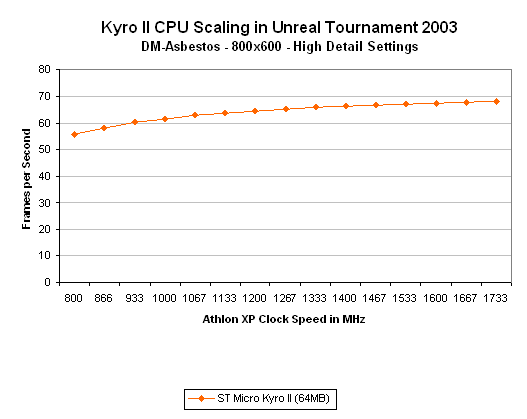
The Kyro II isn’t a fill-rate monster by any definition of the word, its performance is acceptable primarily because of its differed rendering technology. Here you can see that it doesn’t take too powerful of a CPU to drive the Kyro II to its limits, after the 1.13GHz mark the performance curve begins to flatten out.

By moving to Medium Detail settings we shift bottlenecks away from the Kyro II and thus we see a much steeper CPU scaling curve. The Kyro II curve is reminiscent of the GeForce2 curves we saw earlier but keep in mind that you have to be higher up on this curve in order to remain competitive with the performance of a GeForce2 because these tests don’t take into account physics and AI calculations which a Kyro II system has less CPU power to dedicate to.
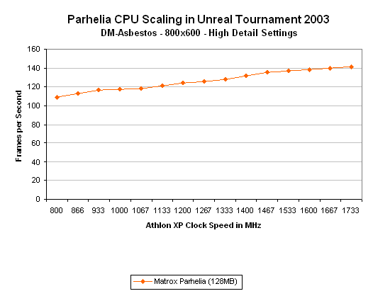
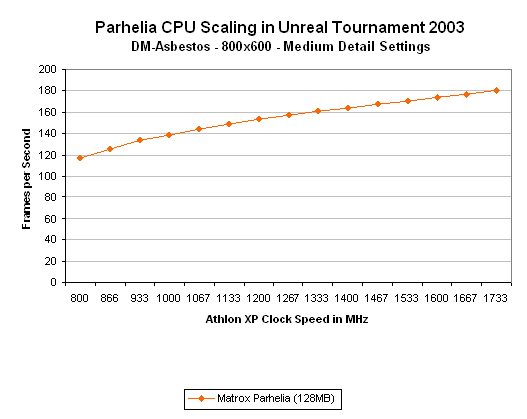
Matrox’s Parhelia
The Parhelia was just recently released and although its installed user base is not significant we included its CPU scaling performance regardless.
Final Words
We refrained from putting all of the cards in a single chart because it ends up being cluttered and you don’t get a good idea for how each individual GPU scales but now that you’ve been through the entire roundup we can leave you with a couple of helpful abridged charts:
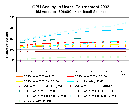
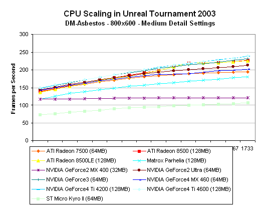
In the end, the results are pretty much as you’d expect; it is the fastest GPUs that truly require very fast CPUs in order to feed them vertex data at a rate that can maintain their high performance levels.
What’s also interesting to note is that if you extrapolate based on this data then you’ll see that the forthcoming generation of GPUs will need even more powerful processors than an Athlon XP 2100+ in order to get the most out of their performance. With AMD slowly ramping the clock speed of the Athlon XP line between now and Hammer’s release, it looks like we’ll be testing R300 and NV30 on Pentium 4 systems.


