Original Link: https://www.anandtech.com/show/9330/exynos-7420-deep-dive
The Samsung Exynos 7420 Deep Dive - Inside A Modern 14nm SoC
by Andrei Frumusanu on June 29, 2015 6:00 AM EST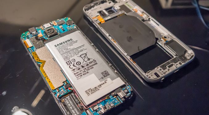
Over the past few years it’s been somewhat expected tradition for Samsung Electronics to employ a strategy of multi-sourcing the SoC for their mobile devices. Most notably it’s on the North American and specifically CDMA markets that we saw wide usage of Qualcomm SoCs. This diversification started with the Galaxy S2 as it was offered both in versions with Samsung System LSI's Exynos chipset as well as variants with Qualcomm’s Snapdragon offerings. On the last few generation of devices we’ve seen the average share of Exynos in Galaxy devices continually decline, as the shift to ARM's Cortex A15 based SoCs just didn’t work out as well in terms of power consumption and thus lost design wins to better balanced Krait-based SoCs from Qualcomm. In fact the last time we’ve seen a Galaxy device make use of an Exynos throughout all its global variants was the Galaxy Note 2 back in 2012.
With the Galaxy S6 again offering a world-wide release of exclusively Samsung designed SoCs, we see an immensely contrasted situation to what we had just over a year ago. The Exynos 7420 marks a true new generation of SoCs for Samsung. The chipset is described as the company’s “most advanced application processor to date”, and today we’re going to have a deep investigation into what a modern SoC looks like, and try to put the chip through its paces through power and performance measurements.
We’ve had a slight glimpse into what the Samsung’s Exynos 7420 might look like when we reviewed the Exynos 5433 in the Note 4 back in the beginning of the year. Attentive readers might remember that as far back as last September I called the Exynos 5433 more of a “brain-transplant” when it comes to SoC-design. This means that it looked like the chipset received an IP upgrade in form of new ARM's A5X series of CPU designs and a Mali T760 GPU, making this only an evolutionary design from other SoCs from last year such as the Exynos 5430 (A15/A7 + T628) and its predecessors. The Exynos 7420 might from a first glance look like nothing more than a process shrink and slight upgrade in the GPU configuration with LPDDR4 memory, but as we’ll soon see there are more details under the hood.
Investigating Samsung's 14nm Process
We’ve heard rumors about Samsung wanting to make a 14nm SoC as far back as 18 months ago. Samsung Semiconductor was historically a follower to TSMC in the leading-edge foundry manufacturing business, so the general consensus among analysts and most of the media was that this was just an unrealistic expectation given the fact that vendors had just started delivering out 20nm TSMC silicon late last year with Apple’s A8 and more recently Qualcomm's Snapdragon 810 and 808. Even though Samsung had presented working 14nm silicon as far back as early October (Which I highly suspect was the 7420) and has in several financial calls confirmed mass production late last year, it still came to many as a shock to actually see the Galaxy S6 be announced exclusively with the 14nm in-house SoC.
The 14nm process marks Samsung's transition from planar transistors to FinFET-based ones. Intel was well ahead of the rest of the industry to make this jump on their 22nm process which shipped in products in 2012, and we should be plenty familiar with the technology by now.
A great deal of discussion ensued over whether Samsung’s 14nm process really represented a “true” die shrink over its 20nm predecessor. We were ourselves surprised to see Chipworks announce that the piece came in at only 78mm² compared to the Exynos 5433’s 113mm². This 31% shrink was beyond what we expected, as we previously reported that Samsung’s 14nm process was to continue to use the 20nm’s BEOL (Back-End-Of-Line, a chip’s largest metal layer) and thus make for only a minor progression. Both the BEOL’s M1 metal pitch and the transistor’s contacted gate pitch equally determine the density and just how much a design is able scale in area on a given process. It was only after Samsung’s ISSCC February 2015 presentation on the Exynos 5433 (Credits to our colleagues at PC Watch) that it became clear as to what is going on:
While Samsung has in the past only referred to the 20nm node as a single process, the reality is that there seems to have been two planned variants of the node. The variant we’ve seen in The Exynos 5430 and 5433 was in fact called 20LPE. In contrast, the process of which 20nm borrows its BEOL from is another variant called 20LPM – and this node sees a very different M1 metal pitch. 20LPM looks to be a cancelled node as it was subsequently dropped in favor of the 14nm processes. We can summarize the differences between Samsung’s recent manufacturing processes in the following table.
| Samsung Semiconductor Manufacturing Processes | ||||||
| 28LPP | 20LPE | 20LPM (Cancelled) |
14LPE | |||
| Nominal VDD | 1.0V | 0.9V | 0.87V | 0.8V | ||
| Logic CPP | 113.4nm | 90nm | 86nm | 78nm | ||
| M1 Metal | 90nm | 80nm | 64nm | 64nm | ||
| M1 * CPP Density | 10206 | 7200 | 5504 | 4992 | ||
Taking the product of the M1 pitch times the contacted gate/poly pitch (CPP) gives an overall representative measurement of process density, and here we incidentally see the same 31% shrink that we saw that happened between the Exynos 5433 and Exynos 7420.
| Samsung Exynos Block & Die Sizes (mm²) |
||||||
| Exynos 5420 (28nm LPP) |
Exynos 5430 (20nm LPE) |
Exynos 5433 (20nm LPE) |
Exynos 7420 (14nm LPE) |
|||
| Big Core | 2.74 | 1.67 | 2.05 | 1.20 | ||
| Big Cluster | 16.49 | 14.50 | 15.10 | 8.88 | ||
| Little Core | 0.58 | 0.40 | 0.70 | 0.48 | ||
| Little Cluster | 3.80 | 3.30 | 4.58 | 2.71 | ||
| GPU Cluster | 30.05 | ~25.00 | ~25.00 | 17.70 | ||
| SoC Total | 136.96 | 110.18 | 113.42 | 78.23 | ||
When we are looking at the block sizes between the 5433 and 7420, we see this theoretical shrink only apply for the individual A53 cores. Both the individual A57 cores and total cluster saw a much large shrink of 59%. The total GPU size also went down by 30% - but keeping in mind that the 7420 has two additional shader cores over the 5433’s MP6 configuration this is also represents a big difference. A single T760 core on the 7420 comes in at 1.75mm², so if we would subtract 3.5mm² from the total area of 17.70mm², we’d end up with a total of 14.2mm for a hypothetical 14nm MP6 GPU – which then again would represent a massive 56% shrink over the Exynos 5433’s GPU if we assume things remained equal on shared common blocks.
This very large ~56%+ shrink of some of the main IP blocks points out that Samsung was not only able to take advantage of the theoretical shrink due to the process, but also further tweaked the physical implementation by either employing more efficient cell libraries or by optimizing the layout for density. When considering the above findings, we can now see how Samsung managed to achieve what is a rather lightweight SoC when looking at the historical die sizes of previous chipsets while still managing to stuff in two additional GPU cores and a LPDDR4 memory controller among other changes.
Evaluation of a process node outside of high-tech laboratories is always a tricky thing as we need to rely on measurable external characteristics such as voltage and power. For some vendors it’s hard to even read out a SoC’s voltages - for example the furthest I was able get with HiSilicon SoCs was to read the PMIC’s register values, but without knowing a buck converter’s indirect mapping to actual voltage it still remains a mystery as to under what operating level the silicon is running at. Luckily this isn’t the case for Samsung SoCs, and in our review of the Galaxy S6 we’ve already been able to present a preview/summary of how voltages were affected when compared to the Exynos 5433 20nm process. To recap some example cases of how voltages have dropped, here’s again a table of operating voltages among a few common frequencies and binning groups of the two chipsets:
| Exynos 5433 vs Exynos 7420 Supply Voltages | ||||||
| Exynos 5433 | Exynos 7420 | Difference | ||||
| A57 1.9GHz (ASV9) | 1200.00mV | 975.00mV | -225.00mV | |||
| A57 1.9GHz (ASV15) | 1125.00mV | 912.50mV | -212.50mV | |||
| A57 800MHz (ASV9) | 900.00mV | 687.50mV | -224.50mV | |||
| A57 800MHz (ASV15) | 900.00mV | 625.00mV | -275.00mV | |||
| A53 1.3GHz (ASV9) | 1112.50mV | 950.00mV | -162.50mV | |||
| A53 1.3GHz (ASV15) | 1062.50mV | 900.00mV | -162.50mV | |||
| A53 400MHz (ASV9) | 787.50mV | 656.25mV | -131.25mV | |||
| A53 400MHz (ASV15) | 750.00mV | 606.25mV | -143.75mV | |||
| GPU 700MHz (ASV9) | 1050.00mV | 800.00mV | -250.00mV | |||
| GPU 700MHz (ASV15) | 1012.50mV | 750.00mV | -262.50mV | |||
| GPU 266MHz (ASV9) | 800.00mV | 668.75mV | -131.25mV | |||
| GPU 266MHz (ASV15) | 762.50mV | 606.25mV | -156.25mV | |||
In the S6 review we briefly described how ASV (Adaptive Scaling Voltage) is Samsung’s denomination for the silicon binning process. Process variations during manufacturing can lead silicon to have different electrical characteristics, leading to cases where a product would no longer be able to function properly under its target specifications. On the desktop space we're familiar with the common practice of disabling parts of the silicon to be able to recycle a “bad piece” into a lower priced SKU. Currently I’m not aware of any semiconductor vendor following this method in the mobile space as there simply isn’t the same opportunity to recycle chips into lower performing SKUs. What does very commonly happen though is that vendors try to increase voltages to compensate for such process variations, overcoming problematic manufacturing issues in this way. Chipsets are tested at the factory for their characteristics and each chip is then permanently marked with the information by burning it to on-chip fuses.
For the Exynos chipsets these bins are called ASV groups. The groups with the higher voltages represent bins with “slow-” or “cold” silicon, meaning process variations cause transistors to not to be fully able to reach the design frequency without having to raise VDD from the nominal targets. One advantage of cold chips is that their static leakage is reduced over other bins. On the other spectrum we have “fast” or “hot” silicon with lower threshold voltages that are able to hit the desired clock-rate at a lower VDD. In contrast to cold silicon, hot silicon has much more static leakage due to the lower Vt. Power consumption in today’s large SoCs is mostly determined by the dynamic leakage (gate to drain, drain-induced barrier lowering, etc) of a chip as it overshadows static leakage currents which can be mitigated by power-gating mechanisms. FinFET also comes into play as it helps to dramatically reduce static leakage compared to planar technologies. It is thus certainly almost always more advantageous to have a “hot / fast” bin which is able to reach lower operating voltages.
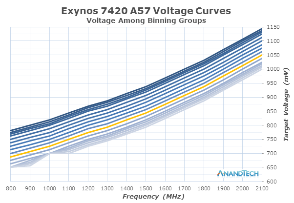
As seen in the graphic, the range between a worst-case and best-case for the Exynos 7420 can be as high as 150mV which represents up to 32% more dynamic power on the highest frequency of the A57 cores. Luckily, one should not have to worry too much about the bin in one’s device as shipped units follow a Poisson distribution pattern where the vast majority of chipsets fall at or around the lambda of ASV10-ASV11. I’ve yet to see a report of somebody receive a device of <ASV6, which doesn’t mean they don’t exist, but they may be very rare. The device which we’ve tested power on in this article came with a chipset graded ASV10 (Highlighted in green in the graph) on the CPU clusters and memory controller and ASV11 on the GPU, which by the way also points out to the fact that the main SoC blocks are individually characterized and don’t necessarily fall in the same grading/bin category.
Until now I’ve been careful to refer to voltages as “target voltages”, and although it’s true that buck converters (High efficiency step-down voltage regulators) on the PMIC may not be fully accurate when providing that voltage, what I’m referring to is another voltage control mechanism outside of the usual software DVFS (Dynamic Voltage and Frequency Scaling) control. For this year, Samsung introduced a new closed-loop DVS (Dynamic Voltage Scaling) system in the Exynos 7420. A closed-loop system is a control system that operates on a feedback loop which continuously monitors inputs through sensors, in this case hardware performance monitors (HPMs). In the case of a DVS system, what we are talking about is a microcontroller which chooses a certain voltage to tell the regulator to apply, and HPMs on the SoC’s various voltage planes. In the Exynos 7420, we see this being arbitrated by an on-chip Cortex M3 microcontroller. Samsung names this the APM- although I’m not sure what it stands for, but strongly suspect it’s either Advanced or Adaptive Power Manager.
The Cortex M3 which we’ll refer to as the APM from now on, communicates with the main system only via small mailbox messages. Mailboxes are one method of inter-processor communication between differing architectures, with each processor can only write messages to their own mailbox (RAM space), but can read all other mailboxes. The overlying software DVFS mechanisms running on the Linux kernel sends target voltages to the APM whenever there’s a frequency change. At first the kernel and main CPU also programs the PMIC regulator directly via an i2c interface, but after the frequency change control is then handed over to the APM until the next frequency change. The APM in turn measures HPMs, one each located on both CPU clusters as well as on the GPU and the memory controllers. When the APM sees the voltage threshold fall, either due to temperature or other influences changing the silicon’s characteristics, it takes advantage of it to further lower the voltages below the values of the stock voltage tables determined by the binning process.
The advantage of the APM over software based solutions by the main CPUs is that it able to have finer granularity and real-time response; it changes voltages at a 1ms interval, compared to the current 20-80ms sampling period the main DVFS mechanism runs at. Voltage steps depend on the PMIC used on the device, for the Galaxy S6’s this means 6250µV granularity on the main buck converters. I’ve noticed Samsung experimented with different margins on how far the APM was allowed to undervolt, and it currently sits at 25mV for the CPU cores and 12.5mV for the GPU and memory interface.
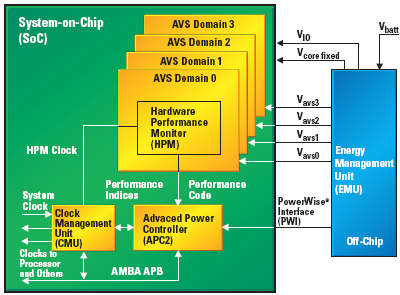
Texas Instruments' PowerWise technology represents a similar closed-loop voltage mechanism (Credit: TI)
What is unusual about this closed-loop voltage regulation system is not the system itself, but the fact that Samsung uses it in conjunction with traditional binning. Texas Instruments was one of the first players in the mobile space to apply CL systems for voltage regulation and was employed in various OMAP SoCs. PowerWise AVS was meant to be used as a power management mechanism – but more importantly it is supposed to cut production cost as it removes the characterization and binning process from the production chain. Qualcomm in the Snapdragon S810 and Nvidia in the Tegra K1 are two other vendors who’ve recently switched over to closed-loop systems, and similarly to TI, they’ve dropped traditional fixed binned voltage tables and rely solely on HPMs to dictate the operating voltages.
Samsung’s 14nm process together with the aforementioned improved voltage regulation systems end up providing a quite massive voltage reduction compared to the Exynos 5433 and previous SoCs. I was curious to see just how low I could go, and was able to achieve down to around 587mV on the A53 cores without taking into account the APM margins. The memory interface is the lowest supplied voltage plane on the 7420, as it operates at a stock value of 575mV up until the 416MHz state before it needs to go higher. The same plane on the Exynos 5433 didn’t go under 750mV.
Earlier in the year I made the comment that while Samsung rolled out 20nm SoCs relatively early compared to other vendors other than Apple, it didn’t really represent a clear competitive advantage as TSMC’s 28HPM process set the bar very high for 2014. Fast-forward only a few months and we see a very different competitive landscape as Samsung beat TSMC to FinFET technology not only by 6-9 months, but actually delivered much more than was initially revealed in the official announcements. It will be interesting how the industry shifts towards the 14nm process as Samsung and process partner GlobalFoundries continue to ramp up production capacity and TSMC also starts to mass produce its own 16nm FinFET node.
The Exynos 7420 - Inside a Modern SoC
At this point in time it’s undeniable that the Exynos 7420 seems to have a clear process advantage over the current competition, but before we go into more benchmarks and detailed power numbers, I’d like to take the opportunity to try to do something we haven’t done before: A dissection of what is actually inside of a modern SoC such as the Exynos 7420.
Over the past few years SoCs have grown more complex and transistor counts have shot up, but we rarely had the occasion to look into what kind of blocks are actually included in such large designs. PR material provided by companies often just include rough simplifications such as CPU core counts or GPU configurations. Some companies such as Qualcomm are even hesitant to give any kind of information on their IP – the Adreno GPU for example remains a mysterious black box when it comes to its architecture. Samsung SoC’s primary processing blocks are relatively well known because they use IP designed by ARM, with whom we have the opportunity and pleasure to extensively cover in articles such as our architectural deep-dives on the Mali Midgard design or ARM’s A53/A57 CPUs. While we feel we have a good understanding of the CPU and GPU, we know little of the remaining SoC components as they never get talked about.
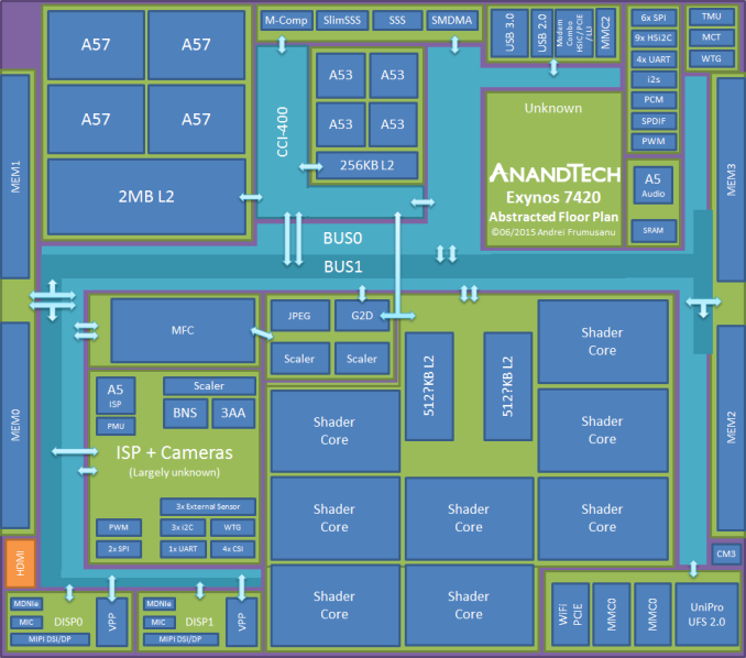
Unfortunately when asking Samsung SLSI about details of the Exynos SoCs, LSI could not publicly comment on the architecture or details of current products. In order to try and learn more about this subject, I tried to reverse-engineer myself through the various IP blocks to re-create a high-level abstracted overview of what the SoC looks like.
Before going into talking about the different blocks and layout, I’d like put a disclaimer out there that this graphic is purely an abstracted plan of the true physical layout. I did have access to a die shot of the chipset to base my analysis on, but we are unable to post this die shot. Blocks such as the GPU, CPUs and memory controllers can be considered to be representative of their actual size and location, other blocks such as the ISP and the top right quadrant are large functional simplifications for the purpose of presentation.
As mentioned in the manufacturing process section, the Exynos 7420 remains a relatively small SoC as it comes in at only 78mm². The biggest IP block is by far the Mali T760 GPU cluster sized at 17.7mm², consuming 22.6% of the SoC, nearly a quarter of the whole die. Historically speaking, this falls in line with what Samsung has previously budgeted for the GPU since the Exynos 5420. The individual shader cores are among one of the largest individual blocks on the SoC as they come in at 1.75mm². All 8 cores are connected via a common fabric and two islands of L2 cache. Samsung has officially disclosed the Exynos 5433’s Mali GPU to come with 512KB of total L2 cache – and size comparisons between the cache islands and shader cores of the two SoCs point out that the Exynos 7420 has a quite larger L2 to shader core ratio, pointing out to the possibility that its size may have doubled up to 512KB per MMU for a total of 1MB. We unfortunately won't know for sure until Samsung eventually releases more information on the Exynos 7420.
Moving on to other IP blocks we have concrete information on, we see the Cortex A57 “big” CPU cluster positioned in one corner of the SoC, largely opposite of the GPU. Again falling back to information released during ISSCC 2015, Samsung explains that this positioning is done for the best thermal management of the SoC. Having the two most power-consuming blocks as far from each other makes sense to try to keep hot-spots to a minimum and maximizing the thermal dissipation potential of the whole SoC.
The Cortex A53 “little” cluster is located right next to the A57 cluster. We see the same configuration as on the 5433 – four A53 cores with 256KB of L2 cache. The 14nm die shrink made it possible to make this the currently smallest modern 4-core cluster among existing SoCs as it comes in at only 2.71mm².
Between the two CPU clusters we find the ARM Cache Coherent Interconnect (CCI-400) that is the core IP that allows heterogeneous multiprocessing between different CPU architectures and is the corner-stone of big.LITTLE SoCs. Besides the CPU clusters, the CCI-400 can also connect three further slave IP blocks to form a group of cache coherent devices. This is the point where things get interesting; there is a general lack of public information from semiconductor vendors on how the CCI and general internal bus architecture looks like. For the Exynos 7420 I was able to confirm at least four of the five possible ports on the CCI.
Again, we have the obvious two CPU clusters each occupying a port on the CCI which is required for heterogeneous and simultaneous operation system of the two clusters. As further CCI slave devices, Samsung chooses to connect the G2D block (On the same port as the GPU) whose full name goes by FIMG2D (Fully Integrated Mobile Graphics 2D), which is the 2D graphics accelerator of Exynos SoCs. The G2D block is part of a larger block dedicated to 2D image manipulation called the MSCL – which is an acronym for M-Scaler although I’m not too sure what the M stands for, maybe Media? The overall block contains two dedicated hardware fixed-function image scalers as well as a JPEG compression and decompression unit. For example video streams will pass through this block to be re-scaled to a display’s resolution.
Another CCI-connected block is a new kind of IP that we haven’t seen before in the mobile space: a memory compressor. Blandly named “Exynos Memory Compressor” or M-Comp this is an interesting specialized piece of IP that has yet to play a role in the Galaxy S6. I’m quite certain this is a hardware block targeted and designed especially for Android. Since Android 4.4 kernel DRAM compression mechanisms have been a validated part of the OS and all devices come with a form or another of the feature. Most vendor devices come with the “zram” mechanism, which is a ramdisk with compression support. The kernel sets this up as a swapping device to store rarely used memory pages. Samsung had implemented this in its Galaxy devices as far back as Android 4.1.
The Galaxy S6 makes use of a more advanced implementation called “zswap” which is able to compress memory pages before they need to get swapped out to a swap device, so it’s a more optimized mechanism that sits closer to the kernel’s memory management core. An everyday example of its effects can be seen when multi-tasking a few apps: a sample readout shows it's able to compress 1.21GB of pages into 341MB of physical memory. Being able to offload the compression to a dedicated hardware block would be a great power efficiency optimization, so we’re hopefully looking forward to a future release and OS update of the device with a software stack that can use the hardware unit.
The memory compressor should be part of a larger block called “IMEM” which contains other elements such as the SSS (Security Sub-System). This is a hardware cryptographic accelerator that has been part of Exynos SoCs since the S5PC110 (Later renamed Exynos 3110) and is able to accelerate encryption and decryption for various ciphers. This includes a DMA engine so that it could directly have disk access for fast full disk encryption. I wasn’t able to confirm if the 7420 physically still has this block as it lacked any drivers. It may be possible Samsung has dropped it in favor of using the cryptographic capabilities of ARMv8, but it would still make sense to maintain a fixed-function IP block for power efficiency.
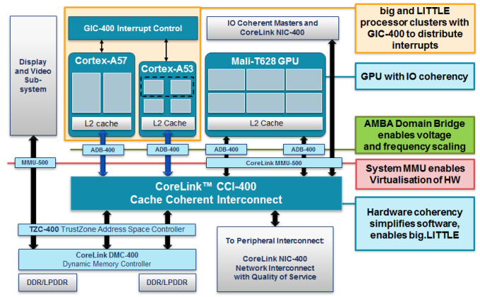
CCI-400 example layout as published by ARM and used in LG's Odin/Nuclun SoC
Exynos line of SoCs do not follow this arrangement.
As mentioned earlier, the one of the CCI ports is shared between the G2D block and the GPU. This is also a large difference to how ARM advertises its example SoC configuration of the CCI: we mostly see Mali GPUs get two ports on the CCI. This makes sense as each port is 128 bit wide in both read and write directions. Vendors have up until now been clocking the CCI at around half the DRAM frequency as most LPDDR3 SoCs saw it running at 400-466MHz. One example SoC which closely follows ARM’s depiction of such a bus architecture is LG’s Odin (Nuclun), as it runs two ports to the CCI running at 400MHz with 800MHz memory controllers. Having a single 128 bit port to the GPU will limit its bandwidth to only half the achievable bandwidth of 2x32bit memory controllers, so that’d be a waste of resources. Furthermore, the Exynos 7420 clocks the CCI at up to only 532MHz. This is an interesting divergence from the DRAM frequency / 2 rule we’ve seen until now, and also means that a single CPU cluster is technically unable to saturate main memory bandwidth on the 7420. The per-port bandwidth is limited to 8.5GB/s in read and write directions for a concurrent total of 17GB/s, a figure we’ll be able to correctly verify later on in the CPU performance section.
The last CCI port which I didn’t actually depict in the layout should go to the CoreSight block, ARM’s system IP for debugging and trace of SoCs.
This leaves the question open on how the GPU is actually connected to the memory controllers. One thing for sure, is that it doesn’t go through the CCI. Samsung calls their internal bus architecture a “Multi-Layer AXI/AHB Bus Architecture”. AXI and AHB are both specifications defined in ARM AMBA (Advanced Microcontroller Bus Architecture), an interconnect standard used in one way or another basically all of today’s SoCs. We know that there is at least a large 2-layer separation: An “Internal” bus which I depict in the SoC schematic as BUS0, a “Memory Interface” bus depicted as BUS1. There is also a less important peripheral bus that I left out due to it connecting smaller low-bandwidth IPs that are not as interesting to the discussion.
The memory interface bus operates on the same clock plane as the actual LPDDR4 memory controllers, reaching up to 1555MHz. The memory controllers physically are spread along two sides of the SoC die. Each memory controller has 2x 16bit interfaces directly to the DRAM dies. This means that the DRAM PoP module contains 4 DRAM dies, standard among 64-bit total bus width SoCs. The most trouble I’ve had in deciphering how the internal bus layout works was trying to understanding how the memory controllers interact with the various buses. It’s clear that Samsung’s bus architecture is quite more complex to the more simplistic designs we have public information about. Sadly, unless there will be future new resources we can fall upon on, the best we can do is to just have a guess on how main traffic flows throughout the chip.
Part of the internal bus blocks are all major I/O IP blocks. These are physically separated into two major blocks called FSYS0 and FSYS1. This includes 3 Synopsis DesignWare MMC controllers (2x 8bit, 1x 4bit) that can be used for eMMC, WiFi SDIO and external SD card connections. A MIPI UniPro controller for UFS 2.0 is of course also part of the interfaces for storage and is used for the NAND storage on the Galaxy S6.
Over the last year we’ve seen WiFi connectivity make a migration from SDIO interconnects to PCIe-based ones. Both Qualcomm and Samsung also did this migration for their top-end SoCs as they included PCIe controllers. The Galaxy Note 4 was one of the first phones to make this switch with Broadcom’s BCM4358 WiFi SoC. According to Broadcom, the reasons for this are two-fold. The first is for performance, as PCIe has significantly reduced processing overhead and DMA capability. The second is power efficiency, as the PCIe spec allows for lower and more fine-grained low power states than the SDIO interface.
The Exynos 7420 - Inside a Modern SoC - Continued
An interesting part of the connectivity blocks is the modem connectivity block. Samsung describes this in its drivers as a “Combo PHY” capable of HSIC, PCIe and MIPI LLI. Given the wide range of connectivity options for external modems and the fact that usually there’s only one modem connected in a device, it makes sense to try to consolidate the various standards to save up on die space. The Galaxy S6 comes for the first time with a global rollout of Samsung’s own modem: Shannon 333. The piece which will probably be marketed as Exynos Modem 333, but like the 7420 Samsung has to yet to publicly acknowledge its existence. The company's in-house modems have in the past seen only limited adoption and used mostly in their home market of Korea. Starting with last year’s push of the Galaxy S5 Mini, we saw Samsung for the first time doing a wide-range rollout to other global markets.
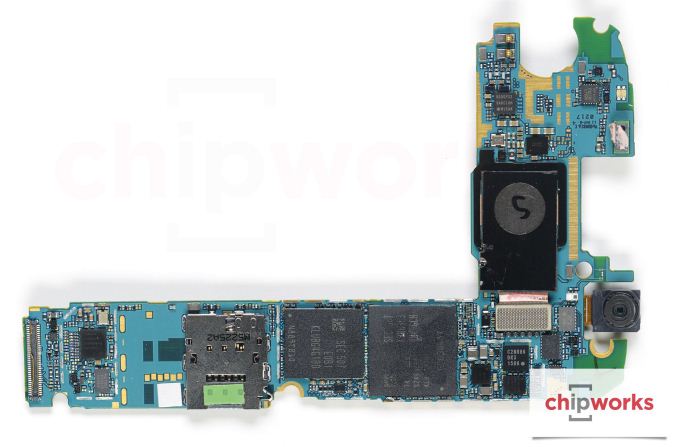
Galaxy S6 PCB with SoC+DRAM and modem+NAND in view. The UFS module sits on top of the modem.
(Image source: Chipworks)
The Shannon 333 is connected to the Exynos 7420 via MIPI LLI (Low Latency Interface). This is an important distinction over past implementations that could have implications on the “integrated vs external” modem discussion. Qualcomm has had an indisputable superiority over competitors due to being able ship an all-in-one solution chipset. The advantage came in two areas: First was due to having a single physical chip; QC had the edge in packaging costs and PCB area footprint. Second one was that external modems require their own dedicated memory to be able to operate. We’ve seen this in many modems in the past, and even Qualcomm’s own Gobi modems such as the MDM9235 need to be partnered with an additional 128MB LPDDR2 of memory. The LLI connection, as opposed to traditional HSIC (High Speed Inter Chip, a USB 2.0 derivative without analog transceivers) interfaces allows the modem to directly access the SoC’s main memory, solving what was one of the most significant overheads of an external modem. Intel was actually the first to have an LLI connected modem in the form of the XMM7260 inside of the Galaxy Alpha, and like the Shannon 333, it was able to ditch the additional memory module which both reduces component cost and power consumption.
While Samsung is unable to comment on this topic, the MIPI Alliance explains that cost and power reduction were the goals of the Low Latency Interface. This also seems to fit with Samsung’s stance on integrated vs dedicated modems, explaining that the latter offers better time-to-market and AP performance characteristics. This makes sense given that modems need regulatory and carrier certifications, a process that takes a lot of money and time. Being able to quickly push out a silicon chip to a production device is critical as the industry now seems desperately to keep up with yearly major refreshes. Also as process nodes get more complex and expensive, it may make sense to actually separate the modem from the main SoC for yield and cost reasons.
It is my opinion that the company will continue with the dual-chip strategy on the high-end, but will still aim to include integrated modems in the low- and mid-range where cost-optimization is absolutely crucial. The Exynos 3470 seen in the Galaxy S5 Mini might see a successor in the ModAP integrated-modem SoC line-up as we’re seeing the first substantial evidence of what the Exynos 7580 is: An 8-core A53 SoC with integrated Shannon 310 modem and LPDDR3 memory. The odd naming convention aside, this looks to be a budget/mid-range chipset aiming to capture some design wins from Qualcomm and MediaTek.
While that was quite a tangent on the modem and its connectivity options, let’s go back to the SoC layout and IP blocks. General connectivity is part of every SoC, and the Exynos 7420 is no different here. With a diverse offering of SPI, HSi2C, UART, i2s, PCM, PWM and other ports it offers all the necessary bus interfaces required to connect all device components to the central SoC. I took the liberty of being very abstract and non-representative with these blocks so one should not read too much into their position or size.
An odd block that I could not account for is a quite larger area next to the A53 cluster. I’m not sure what it represents but it could be an agglomeration of smaller IPs or general SoC logic.
Samsung has used in SoCs previous to the Exynos 5430 a Coarse-Grained Reconfigurable Architecture (CGRA) processing unit called the Samsung Reconfigurable Processor (SRP) for audio processing. The SRP is an interesting architecture that Samsung seems to want to use for a variety of use-cases: We've seen prototype GPUs built with it and Samsung currently uses it as the processing cornerstone of its DRIMe-V SoC in DSLR cameras such as the NX-1. On Exynos SoCs 5430 and newer this audio block was dropped in favour of a more conventional ARM Cortex A5. The companion CPU is in charge of audio decoding, encoding and also audio processing tasks such as equalizer functions. Samsung has previously advertised that it can be also used for voice processing and voice recognition.
Finally, we move on to the media quadrant of the SoC. Here we find the ISP, the hardware media decoder/encoder and the display pipelines.
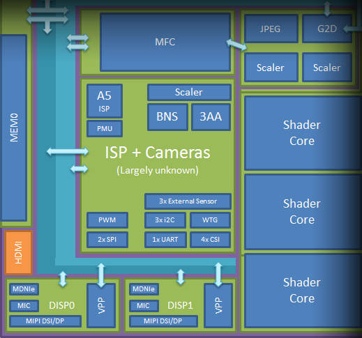
This part of the SoC is depicted totally different than the actual physical layout.
The Exynos’s hardware media accelerator is called the Multi-Format-Codec (MFC). This is a mature block as it has seen implementation in SoCs since the S3C6400 in 2007. Despite being out in the wild for 8 years now, we still don't know much at all about the architecture of the block. My assumption is that we’re most likely looking at a custom DSP architecture as the piece is accompanied by separate firmware that needs to be loaded for operation. The IP is able to encode and decode MPEG4, H263, H264, VP8, and HEVC and can additionally decode MPEG2, VC1 and VP9. The Exynos 5430 and 5433 used an additional HEVC decoder block separate of the MFC to be able to enable playback of the format, but with the 7420 this piece has been subsequently retired from the SoC as its functionality has been merged into the MFC.
I’ve always been impressed with Samsung’s hardware decoder in terms of performance and power, and the v9 of the MFC in the in the 7420 is no exception. I was able to playback 4Kp30 Main HEVC at only about 950mW of total device power (Minimum brightness, portrait mode to try to compensate for display power). This represents about only 600mW of system load power. The CPU load was very low as it hovered around 25-30% at 400MHz on two A53 cores. Unfortunately the decoder isn’t capable of Main10 profile (10bit) playback and freezes up after 2 seconds of 4Kp60 playback, making it not as future-proof as one would have hoped. As a note, Qualcomm’s Snapdragon 810 decode unit has the same limitations, so the playing field for this generation between the two major vendors is even.
Among the collection of media related blocks we find the ISP. We know very little about Samsung’s ISP, but it certainly is a very advanced piece of IP as Samsung can fall back to experience gained not only in the mobile sector but also in the standalone camera market where it produces its custom line of camera SoCs. The ISP consists of a mix of general purpose blocks such as a Cortex A5 running at 668MHz in tandem with a variety of fixed-function units.


Source: Samsung
Most that we know about the ISP architecture is from a 2013 paper Samsung had published on the Exynos 5420’s capabilities. There they explain that the whole ISP is formed by a series of sub-IPs each having their specialized jobs, such as sensor defect compensation, 3A (Auto-focus, Auto-exposure, Auto-white-balance), de-mosaic, inter-frame noise-reduction, phase-detection auto-focus, gyro digital image stabilizer, optical lens correction, face-detection, video stabilizer, and probably an even longer list of image processing features we’re not aware of. The SoC has 4 CSI ports and seems to have support for 3 image sensors.
Finally, we move on to the display pipeline, which Samsung calls DECON, short for Display and Enhancement Controller. The DECON block is also responsible for hardware layer composition. Mobile devices use hardware layers – meaning different frame-buffers on which they draw content to, and let the hardware unit recombine them into the final image. The most common example of this is the Android status bar window. Instead of having to re-render the whole screen whenever there’s activity on the status bar, the system will just redraw the thin status bar and let the hardware units do the composition. Video playback windows and application overlays work in a similar fashion.
The SoC has two main display controllers besides a separate HDMI output. Each is capable of MIPI DSI or DisplayPort output, although I’m not sure what its full capabilities such as resolution and frame-rate are. One addition to the Exynos 7420 that wasn’t present before in past variants is a Video Post-Processor (VPP) on each display controller. I’m again uncertain what the new block does but it seems to be capable of color-space conversions and uses poly-phase filters for a some certain task. Also part of each display controller is a block called MDNIe (Mobile Digital Natural Image Enhancement) which is used on all Exynos SoC for image color manipulation, sharpening and a large number of other effects. This is the block that enables Samsung devices to have different display profiles targeting different calibrations. As a side note, Samsung also employs a similar block on their external AMOLED DDICs to provide functionality to third-party SoCs in devices not using Exynos.
I’ve covered a bit what MIC (Mobile Image Compression) was able to provide to the Galaxy Note 4 in our review of that device; Display resolutions higher than 1080p make the image bandwidth required to transmit data from the SoC to the DDIC exceed the capacity of usual 4-lane MIPI DSI interfaces. To able to drive 1440p and higher displays vendor are either required to double up on the interface to a dual-DSI configuration, effectively using 8 lanes and thus doubling the power consumption of such an implementation. The alternative is to go the route of compressing the stream. Currently Samsung is the only one to offer such a solution in the form of their proprietary MIC mechanism, as the up-and-coming industry standard DSC (Display Stream Compression) has not yet seen compatible products released.
An interesting feature of both implementations that I previously wasn’t familiar with is the capability of doing partial slice updates. This means that if only a smart part of the screen is updated, then the compression algorithm only updates and transmits that part of the image, saving even more power by cutting down redundant data transmissions. I could verify this by changing and exaggerating the image color parameters via the MDNIe block. The display controller wouldn’t explicitly refresh the whole image after changing the color configuration, and only issue a slice update to the DDIC when the clock and WiFi-indicator showed activity. Due to the partial update, only a very small part of the screen would update with the new colors, demonstrating that the SoC transmits only fractions of screen data as static content is buffered directly on the DDIC.
Overall, the Exynos 7420 is an interesting SoC and I hope we’ve been able to better shed some light into most of the significant IP blocks that go into a modern SoC. At 78mm² the 7420 has quite some headroom to grow to the usual size of a high-end SoC. It’s possible Samsung intentionally kept the chip small to get more yield and higher unit volume as it is the first 14nm mass-production chipset for their foundries. It’s also possible that as the $/transistor metric hasn't gone down 14nm FinFET due to it being a very expensive process, that we’re seeing the start of a new trend and the end of large 100mm²+ SoCs. It’ll definitely be interesting to see in what direction the mobile semiconductor vendors will be heading in the coming year as the process gains maturity and production volume further ramps up as Samsung expands and GlobalFoundries and TSMC start their own FinFET mass-production.
We move on to our benchmarking sections with the CPU’s performance and power consumption. We have already extensively covered ARM’s A5x CPU architectures in our detailed review of the Exynos 5433, and interested readers should definitely have a read of that piece if they want to get a good grasp of how ARM’s CPUs in the SoCs were designed. The Exynos 7420 is identical to the 5433 in terms of CPU configuration: We still have four A53 cores and four A57 cores connected by the CCI-400 interconnect. The only difference is in the clock speeds as Samsung now pushes the frequency slightly higher at 1.5GHz and 2.1GHz for the little and big clusters.
CPU Performance: 64-bit Processing
One interesting benchmark that we weren’t able to measure on the Exynos 5433 due it still coming with a 32-bit software stack was the AArch64 performance of the CPUs. To have a look at the impact 64-bit code has on the device we use SPECint2000 compiled for both 32 and 64bit targets on the Exynos 7420. The scores are estimated results and should in not be considered representative of the device’s performance and only show an architectural view of the CPUs performance.
Developed by the Standard Performance Evaluation Corporation, SPECint2000 is the integer component of their larger SPEC CPU2000 benchmark. Designed around the turn of the century, officially SPEC CPU2000 has been retired for PC processors, but mobile processors are roughly a decade behind their PC counterparts in performance. Keeping that in mind it still provides an excellent benchmark for today's mobile phones and allows us to do single-threaded architectural comparisons between the competing CPU designs out there. The scores we publish are only estimates and should not taken as officially validated numbers.
| SPECint2000 base - Estimated Scores Little Cores |
||||||
| Exynos 5433 (Cortex A53) AArch32 |
Exynos 7420 (Cortex A53) AArch32 |
Exynos 7420 (Cortex A53) AArch64 |
Exynos 7420 64 > 32 bit % Advantage |
|||
| 164.gzip | 396 | 432 | 496 | 15% | ||
| 175.vpr | 272 | 290 | 283 | -2% | ||
| 176.gcc | 597 | 674 | 2000 | 197% | ||
| 181.mcf | 291 | 300 | 248 | -17% | ||
| 186.crafty | 448 | 492 | 343 | -30% | ||
| 197.parser | 348 | 373 | 360 | -3% | ||
| 252.eon | 935 | 1092 | 1354 | 24% | ||
| 253.perlbmk | 529 | 588 | 3000 | 410% | ||
| 254.gap | 544 | 611 | 1506 | 146% | ||
| 255.vortex | 529 | 552 | 627 | 14% | ||
| 256.bzip2 | 362 | 395 | 426 | 8% | ||
| 300.twolf | 284 | 306 | 297 | -3% | ||
Starting off with the A53’s performance benefit (or deficit) for AArch64 code, we see a weird phenomenon as the 64-bit results not always outperform the 32-bit variant of the benchmark. Depending on the sub-test, we’re seeing the effect of having to work with 64-bit integers. Tests such as mcf or crafty visibly suffer from the move as the CPU internally has to deal with larger data sizes. There is increased pressure on the caches which slows down the computation speed in these tests. On the other hand, we have other sub-tests which show very large improvements such as gcc, perlbmk and gap as they are able to take advantage of 64-bit registers and other ISA changes for computational purposes. Running such pieces of code brings 2-4x the speedup on the A53 core.
| SPECint2000 base - Estimated Scores Big Cores |
||||||
| Apple A8 (Typhoon) AArch64 |
Exynos 5433 (Cortex A57) AArch32 |
Exynos 7420 (Cortex A57) AArch32 |
Exynos 7420 (Cortex A57) AArch64 |
Exynos 7420 64 > 32 bit % Advantage |
||
| 164.gzip | 842 | 813 | 909 | 927 | 2% | |
| 175.vpr | 1228 | 1120 | 1129 | 1014 | -10% | |
| 176.gcc | 1810 | 1549 | 1617 | 2000 | 24% | |
| 181.mcf | 1420 | 1192 | 1276 | 923 | -28% | |
| 186.crafty | 2021 | 1149 | 1282 | 990 | -23% | |
| 197.parser | 1129 | 841 | 904 | 895 | -1% | |
| 252.eon | 1933 | 2096 | 2280 | 2500 | 10% | |
| 253.perlbmk | 1666 | 1258 | 1363 | 4000 | 193% | |
| 254.gap | 1821 | 1466 | 1506 | 3437 | 128% | |
| 255.vortex | 1716 | 1652 | 1596 | 1681 | 5% | |
| 256.bzip2 | 1234 | 1027 | 1102 | 1102 | 0% | |
| 300.twolf | 1633 | 1260 | 1428 | 1875 | 31% | |
Moving on to the A57 numbers, we again see a similar scenario as the 64-bit vpr, mcf, and crafty show a significant performance downgrade compared to the 32-bit variants due to higher memory and cache pressure. Perlbmk and gap are again the largest benefactors of 64-bit register usage. While the performance boost for the gcc compiler test was significant for the A53 cores, the A57 cores come in at a less impressive but still respectable 28% performance boost.
Overall it’s interesting to see what kind of an impact AArch64 has on performance and it’s clear that the advantages are very architecture and use-case dependent. The two most negatively affected benchmarks were 181.mcf and 186.crafty. The former is based on a single-depot vehicle scheduling algorithm with almost exclusive integer arithmetic that doesn’t take advantage of 64-bit data-structures, so most of performance is wasted due to overhead.
The Galaxy S6 most-notably still employs a 32-bit native browser, and although I'm not sure if this was a deliberate decision or carry-over from existing firmwares, this may be a sign that it may not always be worth to switch over to AArch64 compiled applications.
Memory Latency and Performance
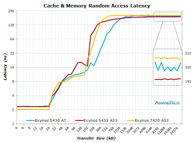
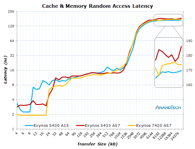
LPDDR4 is one of the major specification upgrades for many high-end 2015 SoCs and the 7420 is along with the Snapdragon 810 one of the first mobile SoCs to adopt the new technology. LPDDR4 doubles its operational frequency over LPDDR3, and the Exynos 7420 runs its memory at 1555MHz (3110MT/s). In terms of computational requirements, CPUs are more sensitive to latency while GPUs require more bandwidth to operate at the best efficiency. As a start, we’ll look at how memory latency has changed on the Exynos 7420. For this review I choose to present the results on a logarithmic scale to better depict the latency differences on the L1 and L2 caches.
The A53 cores don’t show any significant variation in the L1 and L2 results that exceeds the expected 15% difference due to the higher clock-speed of the Exynos 7420’s little cores. As transfer size grows beyond 256kB we see our benchmark leaving pre-fetching and caching on the L2 and hit main memory. Here the Exynos 7420 sees a rise in latency to 206ns over the 5433’s 191ns.
The change in main memory latency is also visible in the bandwidth results of the 7420’s little cores as transfer speeds overall drops on average 10% over what we’ve measured on the 5433.
The latency graphs for the big cores looks more interesting as we see a quite large difference in the L1 cache of the Exynos 7420. The new chip is able to offer a 76% improvement in the L1 latency when compared to the Exynos 5433, as the new SoC is able to hold a very steady 1.91ns versus an average 3.36ns on the predecessor A57 implementation. The frequency advantage of the 7420 comes in at only 10%, so Samsung definitely must have made some changes in the cache architecture as I was able to measure much more consistent latency and bandwidth results in our custom benchmark.
The bandwidth results on the L1 and L2 caches are equally significant: The L1 bandwidth improved on average by 89% while the L2 also saw a 46% increase over the Exynos 5433. NEON load instructions in particular seem have gotten a very large improvement as we’re able to measure a 2.4-3.1x bandwidth boost on the L2 and L1 caches compared to the Exynos 5433’s A57 cluster.
The latency and bandwidth differences are smaller when hitting main memory. The A57 cluster on the new chip actually does better than the 5433 as main memory latency slightly improves by 8ns to 172ns, which results in the same average 4% boost in memory bandwidth using various common access methods. The CPU's are certainly not limited by main memory as they're far from saturating the bus bandwidth on the CCI. As previously mentioned in the SoC layout section, Samsung chooses to limit the CCI to 532MHz instead of going higher to match DRAM speeds. This is contrary to other SoCs and Qualcomm's Snapdragon 810 which runs the CCI at up to 787MHz.
All in all, it seems Samsung may have done some optimizations on the A57 cores that manage to significantly improve their memory performance. One could reason that any performance improvements exceeding the 10% / 200MHz frequency boost, and not affected by possible AArch64 instruction set usage may be result of the higher on-core and cluster cache performance boost, and while that’s hard to verify, we see no other architectural difference between the 7420 and its predecessor.
Off-topic - Galaxy S6 Disassembly Process
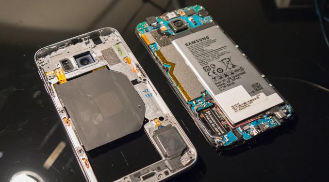
Before I get into the power numbers and explain our methodology, I would like to take the opportunity to share my experience with dismantling the Galaxy S6 and getting access to the battery, as some readers and eventual device owners might be interested to hear about the feasibility of the battery swapping process. The by far most daunting process and time-consuming procedure is the removal of the glass back-cover.
The Gorilla Glass 4 piece is held in place by very heavy-duty glue surrounding the edges of the device. It’s basically required to have a very strong suction cup and at least a hair dryer if one doesn’t have access to a heat gun. I used a car's GPS mount for the suction cup as it provided a tight hold and also acted as a lever to pull on. The glue needs to reach a high temperature to soften up, and you might need to heat up (along the edge) the device until it’s no longer comfortable or possible to hold. One should have some plastic picks ready – I just cut up a plastic SIM-card holder into pieces to use them as picks. The initial prying should start at the bottom of the device opposite of the speaker. The process takes a lot of force before one is able to put the first pick in and it definitely not for the faint-of-heart. Slowly advancing along the edge of the device with repeated re-heating should get you to remove the glass cover from the main body.
Once the back cover is removed, the rest of the process is very easy as we’re just dealing with ordinary Phillips screws. After removing all visible screws one should apply moderate heat along the front edges of the display. While keeping pressure on the battery one lifts up the whole unibody frame of the device from the screen and motherboard assembly. For the normal Galaxy S6 the process is almost over as the battery is now in direct view and accessible, one can disconnect the connector and slowly and carefully pry it up from the sides to separate it from being glued on the display assembly. S6 Edge owners will require further removing of the motherboard as the battery connector wraps around to the back of the PCB.
Once the new battery is in place and properly connected, the re-assembly process becomes straightforward as it is just a reversal of the disassembly steps. One should make sure that the glue strips on the glass back cover don’t have ridges or overlapping pieces as it will cause the back cover to slightly stick out and no longer be level with the metal frame. Once the phone is back together, I would again recommend applying heat along the edges of the device while forcibly squeezing the back glass and whole assembly back in place.
Overall, the whole procedure of replacing the battery should take up to 30-40 minutes depending how much one struggles to remove the back glass. We’ll have to see how Samsung's new battery chemistry holds up after 1 year of constant usage and fast-charge cycles, but if required to swap out the battery it’s definitely a doable process if one manages to muster up the initial courage.
CPU Power Consumption
The power consumption measurements are probably the most eagerly awaited and sought-after part of this piece, as they’re crucial for determining just how much of an effect the 14nm manufacturing process has on power efficiency. To get the numbers, we hook up the Galaxy S6 to an external power supply and energy meter.
Results labeled “load power” represent the difference between idle power consumption and the total power of a given scenario. This means for a given test, we measure the power consumption of the device while it is not doing any activity other than displaying the appropriate screen content. This method allows us to compensate for screen and miscellaneous device component power consumption. By controlling power management and performance of the device we can thus recreate very accurate active power figures for the SoC. One has to keep in mind though that this methodology doesn’t allow us to granularly separate always-used blocks of an SoC such as interconnects or DRAM – so there’s always a slight overhead on top of the IP block we’re interested in measuring power on.
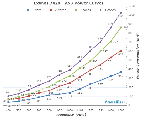
We start by looking at the A53’s cluster and core power consumption. We use a power-virus that creates an artificial load on the CPU cores. This method gives us a good representation of the maximum power consumption at a given frequency, thus detailing the power curve of the silicon at various frequencies and voltage levels. Real-world use-cases will seldom be able to fully load the CPU to such extent, as even high loads will only reach 80-90% of the CPU’s capacity at a given frequency, and thus only consume about the same percentage in power.
Measured power consumption very largely follows the P = C * f *V² formula for dynamic power consumption, where power is a function of frequency times voltage squared multiplied by a constant value representing capacitance of the IP block. Semiconductor vendors also follow this formula in their thermal management drivers as they model the estimated power consumption.
We see that the little cores on the Exynos 7420 use up to 1W when loading up 4 threads on the cluster. This is a slightly higher value than what we saw on the Exynos 5433, but could be explained by the fact that the CPU is running at a 200MHz higher frequency state. Top voltage on the Note 4 unit I measured piece reached 1150mv while the Galaxy S6 tops out at 1037mV. A quick calculation of the fV² factor of the dynamic power formula points out to a value of 1613 for the 7420 and 1719 for the 5433, meaning that if we would just consider voltage and frequency the 7420 should definitely consume less power even at the higher clock rate. The logical explanation is that we’re seeing increased capacitance due the new chipset's implementation and layout. Capacitance can be deducted by verifying that the remaining missing term after fV² results in a steady constant value among all measurement points – and indeed it looks like the A53 cores on the Exynos 7420 have 30% higher capacitance than what we saw on the 5433.
An odd behavior that I’ve already measured on the Exynos 5430 is that the power increase diminishes with every added thread. ARM at the time had explained to me that this was caused by the A7 cores fighting for cluster resources and that each added thread would result in diminishing returns as each core would do less work (and thus consume less power). Supposedly the A53’s new architecture in the 5433 was able to handle the load much better and avoid this bottleneck and that is why we were able to see even increases in power with each added thread. Yet the 7420 exhibits the same issue as seen on the 5430, pointing out this may not have been an architectural characteristic of the cores after all. I’m not too sure what to make of this behavior and probably only Samsung knows the exact behind-the-scene changes that lead to it.
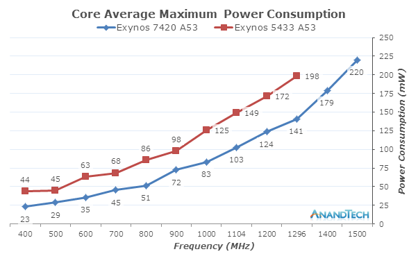
The core average maximum power consumption is the average between the power differences of core 1-2, 2-3 and 3-4. This metric is lower than the 1-core results of the power curve graph because it tries to account for the power overhead of the non-CPU consumption such as cluster, interconnect and memory which come out of their low-power states when the CPU is doing work. Even though the maximum power for the Exynos 7420’s A53 cores is higher than the 5433’s, it manages to beat the 5433 by 30-40% on a per-frequency efficiency basis. The massive voltage drop that the new 14nm FinFET brings to the table is enough to outweigh the increased capacitance of the cores.
A non-trivial part of the power figures that I’m not able to properly measure is the static leakage of the SoC. I tried to reach out to Samsung to comment on the improvement, but wasn’t able to get a concrete answer in regards to their SoC products.
| Device Minimum Screen-on Power (~2 cd/cm² Brightness) |
||||||
| Device | Power Consumption (mW) | |||||
| Galaxy S5 (Snapdragon 801) | 258mW | |||||
| Galaxy S5 LTE-A (Snapdragon 805) | 354mW | |||||
| Galaxy S6 (Exynos 7420) | 358mW | |||||
| Galaxy Note 4 (Exynos 5433) | 452mW | |||||
| Meizu MX4Pro (Exynos 5430) | 530mW | |||||
| Huawei P8 (Kirin 930) | ~500mW | |||||
The Note 4 Exynos turned on black screen and idling consumed a minimum of 440mW while the S5 LTE-A (S805) uses 354mW. Other devices such as the Meizu MX4Pro or the Huawei P8 bottom out at respectively 530 and 500mW. The S6 on the other hand reaches down to only 330mW, a significant 25%+ reduction over other handsets, but still not enough to beat the efficiency of last year's Galaxy S5 which came in at only 258mW. This is an important metric as this is a power value that represents a non-avoidable constant drain whenever you actively use the device (Deep sleep states when the screen is off will power-gate most of the SoC and turn off other device components).
Besides the SoC, the display controller IC is one of the main power drains while it drives the pixel matrix of either LCD or AMOLED devices. ARM had previously shared with us that measuring the dedicated voltage rail of the display assembly on a Galaxy S5 lead to power values of around 90mW when displaying pure black. This value must have subsequently gone up as devices moved to 1440p resolution screens.
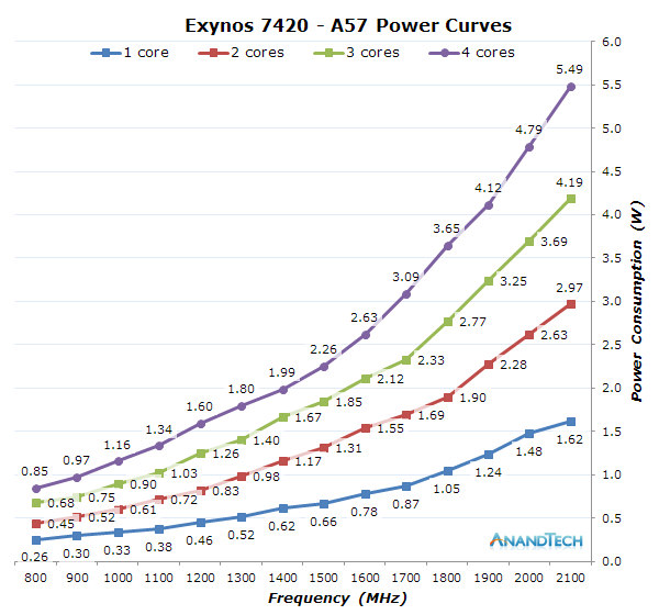
Moving on to the A57 cores we should be seeing some big improvements in power consumption. I’ve mentioned in the Note 4 Exynos review that I thought Samsung shipped the 5433 with too high clocks as the increased power consumption may not have been worth the small performance boost of the last 200-300 MHz. We first have a look at the variable thread-count power curves:
Maximum power consumption of the A57 cores comes in at 5.49W – a much more reasonable figure than the 7.39W seen in the 5433. When we look at the per-frequency power numbers this difference becomes even more significant as 1.9GHz on the 7420 uses only 4.12W compared to the 7.39W of the 5433. Similarly to the A53 cores, Samsung was able to take full advantage of the new process node as the maximum CPU voltage drops from 1.235V at 1.9GHz down to 1.037V at 2.1GHz (0.962V at equivalent 1.9GHz). The bottom frequencies see even larger reductions as we go from 900mV down to 675mV on the 700/800MHz states.
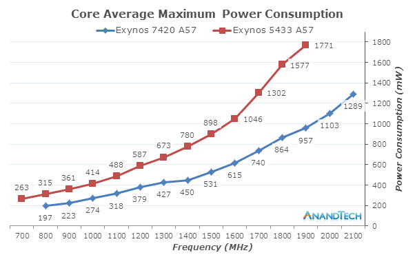
The core average maximum power consumption gives a simplified view the power curve. Here we see the drastic reduction in power the Exynos 7420 is able to provide as we see an overall decrease of 35-45% throughout the frequency curve. At 1900MHz the 7420 falls just a bit short of half the power of the 5433, which is impressive. Capacitance on the A57 also went up a bit; I was able to derive an average of 10% higher capacitance on the new chip, which isn’t quite as high an increase as on the A53 cores, but still a curious change in the physical characteristic of the new implementation.
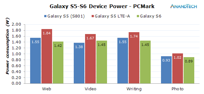
PCMark is a great benchmark that shows of different kind of use-cases that one would daily encounter when using a smartphone. Thus it offers a great repeatable test-bench which can measure overall device efficiency. We measure the whole device's power as we cannot factor out the screen's power for on-screen dynamic tests, so this is also an apples-to-apples comparison to other devices we have figures on such as the Note 4 and MX4Pro.
Overall device power during the tests is very good. It's especially the web test which offers largest improvement over other devices as total power comes in at only 1.42W, over 1W less than the MX4Pro and Note 4. Overall the Galaxy S6 is currently the most least power consuming device I've yet come to measure, which should be very encouraging for the power metric of the device and SoC.
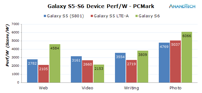
When taking into account the scores the device was able to achieve, we see an even greater improvement over past devices. The performance per Watt figures which depict efficiency are across the board 1.5-2x better than what we see in other devices. Of course the Galaxy S6's shows improved OLED efficiency as part of the whole package, but to be able to post such significant imrovements is nonetheless impressive. It's now understandable why Samsung deemed that a 2550mAh battery was enough for the Galaxy S6 as the device is able to use the available energy much more efficiently.
One of the first things I did when receiving my S6 review unit was to compile a custom kernel with access to the SoC’s voltage tables and try to see how far the chip allowed me to reduce voltages. Undervolting, much like overclocking in the PC space, is a popular modification for enthusiast users that like to tinker with their devices to try to squeeze out as much potential as possible. For mobile device we’re trying to aim for more power efficiency instead of more performance as today’s devices in a way already come overclocked at much higher maximum frequencies than what they’re able to sustain in terms of thermal loads.
| Exynos 7420 Undervolting Results 4-Core Load Power (mW) |
||||||
| A53 Cluster | A57 Cluster | |||||
| Freq. (MHz) |
Stock voltage |
-50mV | -75mV | Stock voltage |
-50mV | -75mV |
| 2100 | - | 5481 | 4911 | 4661 | ||
| 2000 | - | 4781 | 4331 | 3991 | ||
| 1900 | - | 4111 | 3671 | 3441 | ||
| 1800 | - | 3641 | 3111 | 2944 | ||
| 1700 | - | 3089 | 2677 | 2500 | ||
| 1600 | - | 2621 | 2312 | 2186 | ||
| 1500 | 1026 | 916 | 894 | 2254 | 1928 | 1882 |
| 1400 | 859 | 768 | 743 | 1964 | 1791 | 1664 |
| 1300 | 699 | 634 | 625 | 1793 | 1577 | 1444 |
| 1200 | 606 | 536 | 509 | 1590 | 1351 | 1259 |
| 1100 | 491 | 459 | 424 | 1330 | 1151 | 1069 |
| 1000 | 391 | 354 | 337 | 1153 | 1009 | 921 |
| 900 | 340 | 298 | 277 | 969 | 829 | 761 |
| 800 | 270 | 230 | 221 | 843 | 695 | 690 |
| 700 | 225 | 192 | 180 | - | ||
| 600 | 172 | 139 | 128 | - | ||
| 500 | 132 | 108 | 98 | - | ||
| 400 | 104 | 79 | 71 | - | ||
To keep things simple, I measured power on the A53 and A57 cores when applying a global -50 and -75mV undervolt over the stock voltages of the individual power planes. As can be seen in the table, one can gain significant power efficiency as one reduces voltage. The theoretical reduction in power is easily calculated if one has the stock voltages and original power consumption at hand. It is possible estimate the power after undervolting by using the following formula:
PUndervolt = POriginal / (VOriginal² / VUndervolt²)
For example on the 2100MHz state of the A57, this would come to: 5481mW / (1.037V² / 0.987V²) = 4965mW. The measured power indeed comes near that value at 4911mW. The difference should be explained due to factors we’re not taking into account in the simplified formula for power consumption as we’re disregarding static power leakage scaling, and most importantly in this case, temperature scaling.
This can be verified in the lower frequency states which dissipate a lot less power, such as the 1GHz A57 state: 1153mW / (0.712V² / 0.662V²) = 996mW, closer to the measured 1009mW.
I was able to go down to a global -87.5mV global undervolt before the device would crash and fail. It is generally difficult to find the minimal stable voltages for undervolting as it takes weeks to be able to fully test stability for a given voltage at each frequency. Again, it’s SoC temperature which is the big unknown variable here, as a transistor’s voltage threshold rises the colder the silicon gets. An undervolt can be unstable and crash the device if one leaves it to cool down below a certain level, while at the same voltage it can be perfectly usable in active usage or when it’s not allowed to cool down too much such as in one’s jeans pocket. For actual usage it’s always preferred to raise the voltages back up a step or two when one has identified an instability. Samsung’s closed-loop voltage control is an interesting new mechanism for undervolting as it allows further reducing of the safety margin without sacrificing stability. Since reassembling the S6 I’ve been using it as a daily device on a static -50mV across most frequencies and increased the voltage threshold the APM was allowed to undervolt up to -37.5mV, providing the best of both worlds.
Power Management
Power management of previous big.LITTLE SoCs from Samsung was disappointing as it showed little signs of optimizations for efficiency and a general of attention to detail. The Exynos 7420 improves on this in several areas, some which are tied to the 14nm improvement and others which are tied to software improvements.
Modern ARM CPU’s power management works in a few different ways. Firstly, DVFS (Dynamic Voltage and Frequency Scaling) mechanisms try to optimize power efficiency by running the lowest possible frequency state without impacting performance. Because lower frequency states require lower operating voltage they intrinsically use less energy for a given fixed workload. The switching between these P-states (Performance states) is arbitrated by a so-called CPU frequency governor which works within the Linux kernel’s CPUFreq framework.
Google has since Android 4.1 Jellybean standardized the use of the “interactive” CPU governor as a part of Android and the vast amount of devices out there adopt this as the default governor, although vendors may have modifications done to it. The interactive governor is a relatively simple concept: Given a certain sampling time (20ms), it checks the load of the CPU. If the load exceeds the target load on the current frequency, then change to a frequency that would accommodate the current load within the target load threshold. The target load threshold is a parameter which describes how much % of CPU capacity we want the CPU to be at when scaling up to a certain P-state. If the load spikes too fast and much is superior to the target load, then there’s a secondary threshold called the high-speed load threshold which forcefully scales the CPUs to a fixed higher frequency, which in the case of the Exynos 7420 is respectively 900 and 1200MHz for the A53 and A57 cores. If the load has been stable and the newly computed target frequency is consistently aiming lower for 4 sample periods, meaning 80ms, it then scales back frequency to a lower state.
Samsung tries to optimize the Interactive governor to improve big.LITTLE scaling by introducing some new operating modes which alter the configurables of the interactive scaling logic on-the-fly. For example if only a single big CPU passes a load threshold of 95% it enters “single-load” mode which reduces the scaling thresholds for easier increases in frequency and also sets up a quality-of-service minimum frequency request to the small cores. I’m not too sure why they forcefully raise the frequency on the small cores when load is high on the big cores but Samsung must have profiled frequency scaling and decided that this is a beneficial change. Another mode triggered on top of the single-load mode is when the cumulative load across all 4 CPUs exceeds a certain threshold. This multi-load mode again changes scaling parameters by making them more lax and easier to scale up.
These changes had already been implemented in the Exynos 5433 as well but were never effectively used as the parameters remained at their default values and thus representing no improvement in the scaling mechanism. The Galaxy Alpha's 5430 did have the settings correctly set up, but then again Meizu's MX4Pro didn't, meaning we're either seeing an unlikely deliberate design decision, or what I find more likely and reasonable explanation, an oversight on the part of the software teams.
It looks like these modifications are mostly aimed at improving performance and reaction time of the DVFS scaling, and it looks the due to these changes the Exynos 7420 behaves much better in that regard. Samsung’s handling of frequency scaling is generally very good as the governor does well in its task. There are also a large number of QoS (Quality-of-Service) mechanisms by a variety of drivers which are able to instantly request the CPU to transition to a minimum frequency. One example is the screen touch booster: this is an independent scaling mechanism that is able to control the CPU frequency of both clusters as well as to tell the scheduler to force migrations onto the big cores for better reaction time and UI fluidity as soon as the display driver receives an interrupt request from the touch controller. Another scenario would be IP blocks in the media pipeline – blocks such as the 2D composer or the hardware video accelerator are predictable in terms of the required memory bandwidth and CPU capacity, so their drivers will dynamically put performance floors on the device’s DVFS mechanism to guarantee throughput. Samsung goes as far as to also use a QoS system for I/O bandwidth for the NAND, modem and WiFi as well as IPC (Inter-process calls) communications.
Of course beyond DVFS scaling as a power management mechanism all modern devices also offer clock- and power-gating. For the CPU this is again something which is controlled by the kernel within a mechanism called the CPUIdle framework. In the past before hardware had such power-saving mechanisms idling a system usually meant that it was running infinite loops of NOPs (no operation) until it got interrupted to do some actual work. Today instead of running inefficient idle loops, the scheduler calls the CPUIdle governor telling it to do “nothing”. The CPUIdle governor accumulates statistics on how long each idle period is and based on this data is able to choose from a variety of deeper or shallower hardware idle states. On ARM CPUs since the A15/A7 this is mostly consolidated into 3 so-called C-states: a clock-gating state called WFI (Wait-for-interrupt), an individual core power-gating state and a cluster power-gating state.
WFI is an instruction-level and architectural power-management state with extremely low latency that stops the clock to a given CPU. By stopping the clock one avoids dynamic leakage by the CPU, so this is a crucial part of doing “nothing” in mobile CPUs. Individual core power-gating states are able to turn off power to the CPU this way. This is a deeper state as the CPU needs to save its state upon entry and restore it upon waking up. On the 7420 we’re talking about exit latencies of 100µs. Because of the overhead of restoring the CPU state, it’s also not worth to enter these modes for reduced periods of time (called residency time). For the A57 cores this residency threshold is 2000µs and for the A53 cores 750µs. When all cores within a cluster are idle the whole cluster is allowed to be powered down. This of course has larger overhead with larger exit latencies (300µs) and greater minimal residency times (5ms). The cluster power-down is largely used on the big cluster as the small cluster is only allowed to power itself down when the screen is off. A very low-hanging fruit which has finally been picked by Samsung is to have optimized configuration values for each cluster. Previous Samsung SoCs would oddly just use a single driver with the same settings for both clusters, which didn’t make much sense and likely impacted CPU idle efficiency.
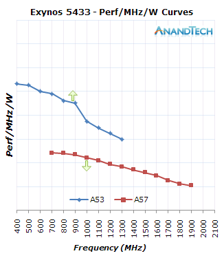
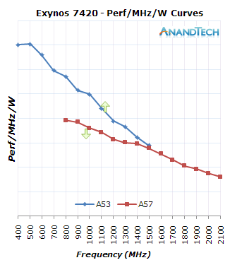
The 14nm process seems to have introduced a change in dynamic between the two CPU clusters as the efficiency of each cluster has scaled differently. This has significant impact in the way the GTS scheduler settings are set up as the new chipset’s power efficiency curves are tighter to each-other when compared to the Exynos 5433. To demonstrate this, I took the SPECint2000 scores of each cluster to determine what the IPC difference between the two architectures is and then used this as a ratio to normalize the A57 perf/W curve to the A53’s clocks. On the first set of charts the vertical axis is just an arbitrary normalized value of MHz/mW for the A53 cores, and the A57 curve uses a multiplier ratio of 2.09 to scale the efficiency value and thus represent the IPC increase of the larger architecture.
I’ll get back to actual perf/W charts in just a bit, but first I want to explain why the perf/MHz/W curves are an important metric we can deduce a lot from. Currently the Linux kernel and GTS mechanism sees load on a frequency invariant scale; what this means that if a process takes up 50% of the CPU while it’s running at 500MHz and its maximal scaling frequency is 1GHz, the scheduler will account the task as a 25% load on that CPU. This mechanism is meant to normalize current load to the maximum possible capacity of a CPU, and not just the current one.
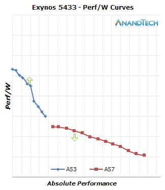
The trigger points that determine thread migrations in GTS are called the up- and down-thresholds, which are thresholds on the load scales of the CPUs. For the Exynos 5433 Samsung used 50% and 25% as the up- and down-thresholds. When a thread would exceed 50% of the A53’s capacity it would be migrated over to the big cores, and once on the big core if the task would fall below 25%’s of the CPU’s capacity it would then migrate down. On the 7420 these values are set up slightly differently as Samsung configured the default values at 46.7% and 20.8%. At first I was confused to see such specific values and didn’t fully understand why they were set up as such until I calculated the actual performance/W curves of both CPU cluster.
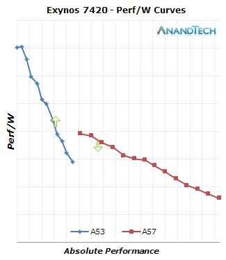
One will have noticed the arrows I put on the graphs – these represent the theoretical point where a thread should migrate up to the big core, or down to the little cores. For the very attentive readers they will notice that the up threshold arrows aren’t at the mentioned 50 and 46% frequency points of the little cores. This is because the CPU frequency governor should actually be able to scale up frequency faster than the task triggering a scheduler migration by hitting the normalized up-threshold. For example 50% up-threshold of the 5433 would mean a 100% load at 800MHz of the A53 cores, but that will realistically never happen as the CPU will have scaled up to a higher frequency by then. The 5433 governor will try to maintain 10% of idle capacity when scaling to a frequency while the 7420 seeks 25%, meaning the latter has more lax settings which make it scale higher in frequency even though the load doesn’t require it. The result is that the avarage effective performance/capacity point where the little CPUs will try to migrate to the big cores is slightly below 900MHz for the 5433 and just above 1100MHz for the 7420.
For the down-threshold of the big cores the logic is a tad simpler because the scaling-down mechanism of the frequency governor is slower than the scheduler’s migration mechanism. This means that the arrow depicted in the graphs is a minimal value of when a thread will migrate down, and a down-migration might happen anytime at the higher frequencies.
When plotting the efficiency points on an axis depicting the absolute performance of the cores we get a much clearer picture of what big.LITTLE is supposed to achieve. And this is where we see a large difference between the 5433 and 7420: The way the Note 4 is currently set up makes it migrate up threads sooner than compared to the Galaxy S6 and the efficiency degradation when doing so is much greater. An optimal implementation would be a device where the up- and down-migration points would be as close as possible to each other in the efficiency axis while having a slight jump in the performance axis acting as a hysteresis to avoid migrations when a load falls in between the two performance curves.
It seems to me that Samsung paid much better attention to efficiency optimizations on the Exynos 7420’s software as it fixes many of the weird configuration issues of the Note 4 Exynos. The Exynos 7420 joins the Exynos 5430 (And MediaTek’s MT6595 which I’ll hopefully address sometime soon) as one of the rare SoCs which are able to reign in ARM’s big CPU core designs in a small form-factor mobile device and effectively use big.LITTLE without major downsides. While Samsung’s software stack could definitely improve with features such as full energy awareness inside the scheduler, it's no longer as misconfigured and as bad as I decribed it in the Exynos 5433 review.
In terms of maximum power consumption, I think 1.9GHz would have been a slightly more reasonable cap for the A57 cores as the device can on some occasions such as updating many apps or visiting a very heavy ad-ridden site can load up the big CPUs to their full capacity and make the device run a bit hot, but it’s a rare occasion and the vast majority of processing time is spent on the lower frequencies. It will be interesting to see what ARM's A72 processor core will be able to achieve in terms of performance and power efficiency. For 2015 though it seems Samsung's A57 SoC still remains king due to its process node advantage.
GPU Performance & Power
Continuing on to the GPU side of the Exynos 7420, we’re again revisiting ARM’s Mali T760. We’ve extensively covered ARM’s Midgard series and Samsung’s implementation in our in-depth architectural article as well as the Note 4 Exynos review. The Exynos 7420 isn’t too different to the 5433 on the GPU side other than having 2 additional shader cores and being able to take advantage of LPDDR4 memory. While we’re pretty sure of the impact the two added shader cores will have, the new memory technology and increased bandwidth it brings is still an unknown until we take a deep look at how performance scales with the faster memory.
First we take a look at peak power consumption of the 7420 and how it compared to other SoCs we currently have numbers on. For this we measure power during GFXBench’s T-Rex and Manhattan 3.0 tests in off-screen mode.
The Galaxy S6 and Exynos 7420 use up to 4.85W of load power. Again, load power here means the figures have the device’s idle and the screen power consumption subtracted to give a better view of the active SoC power instead of the device as a whole.
The 14nm manufacturing process looks to have allowed Samsung to increase performance while still improving power over the 5433’s T760MP6 which runs at slightly lower clocks. We previously investigated Samsung’s curious DVFS technique for ARM’s Midgard architecture and it seems the Exynos 7420 does a much better job at balancing out power when the GPU handles ALU-heavy loads. As a reminder, Samsung chooses to clock the GPUs higher whenever a given task puts a more ALU-centric load on the shader cores. In the case of the Exynos 7420 the GPU runs up to 772MHz in this mode while loads which stress the texture- and load/store-units cap the maximum frequency at 700MHz. On the Exynos 5433 for example these limits were set at respectively 700 and 600MHz, so the 7420 has a comparatively smaller boost. The voltage difference between the two top states is also not as high as on the 5433, and both factors combined result that the GPU power difference between high-arithmetic and normal loads is minimal.
I finally had the opportunity to measure Qualcomm’s Adreno GPU's in the form of the Snapdragon 801, 805 and 810 in the S5, S5 LTE-A and G Flex2, and it showed some revealing numbers that I hadn’t expected. Firstly, it’s now very clear how the Adreno 420 was able to outperform the Mali T760MP6 between the two Note 4 variants as the power and efficiency difference on the T-Rex test is significant. What is interesting to see though is the Adreno 4xx's much higher power draw on ALU heavy loads such as the Manhattan test. While the Midgard architecture seems to allow the GPU a power advantage in arithmetic loads, the Adreno 4xx sees the complete opposite as its power draw increases dramatically.
To have a better picture of overall efficiency between the various architectures, I laid out both the performance and power numbers in a table overview:
| T-Rex Offscreen Power Efficiency (System Load Power) |
||||||
| Mfc. Process |
FPS | Avg. Power | Perf/W Efficiency |
|||
| Exynos 7420 (S6) | 14LPE | 56.3 | 4.82W | 11.63 fps/W | ||
| Snapdragon 805 (S5LTEA) | 28HPM | 40.7 | 4.06W | 10.02 fps/W | ||
| MT6595 (MX4) | 28HPM | 23.3 | 2.42W | 9.55 fps/W | ||
| Snapdragon 810 (G Flex2) | 20SoC | 45.5 | 4.84W | 9.39 fps/W | ||
| Exynos 5430 (MX4Pro) | 20LPE | 28.7 | 3.55W | 8.08 fps/W | ||
| Snapdragon 801 (S5) | 28HPM | 26.9 | 3.47W | 7.77 fps/W | ||
| Exynos 5433 (Note 4) | 20LPE | 37.3 | 5.35W | 6.97 fps/W | ||
| Exynos 5430 (Alpha) | 20LPE | 31.3 | 4.88W | 6.41 fps/W | ||
| Kirin 930 (P8 Estimated) | 28HPM | 17.0 | 3.69W | 4.60 fps/W | ||
While the Exynos 7420 draws a high amount of power at 4.82W, it also is able to post by far the best performance and thus ends up at the top of the efficiency table. While Qualcomm’s S805 has a full two process node disadvantage over the 7420, it is still able to just trail it in terms of power efficiency in the T-Rex test. The Adreno 430 of the Snapdragon 810 manages trail behind the Snapdragon 805 in efficiency even though it's on a better process node.
Things get shuffled around a bit in the more demanding and arithmetic heavy Manhattan test:
| Manhattan 3.0 Offscreen Power Efficiency (System Load Power) |
||||||
| Mfc. Process |
FPS | Avg. Power | Perf/W Efficiency |
|||
| Exynos 7420 (S6) | 14LPE | 24.8 | 4.87W | 5.08 fps/W | ||
| Exynos 5430 (MX4Pro) | 20LPE | 12.3 | 3.20W | 3.84 fps/W | ||
| MT6595 (MX4) | 28HPM | 8.1 | 2.15W | 3.76 fps/W | ||
| Snapdragon 805 (S5LTEA) | 28HPM | 18.2 | 5.20W | 3.66 fps/W | ||
| Snapdragon 810 (G Flex2) | 20SoC | 22.2 | 5.82W | 3.34 fps/W | ||
| Snapdragon 801 (S5) | 28HPM | 11.9 | 3.75W | 3.17 fps/W | ||
| Exynos 5430 (Alpha) | 20LPE | 12.7 | 4.07W | 3.11 fps/W | ||
| Exynos 5433 (Note 4) | 20LPE | 17.5 | 6.08W | 2.87 fps/W | ||
The Exynos 7420 remains at the top as the most efficient chipset, but this time it managed to do this by a considerable margin as Qualcomm’s Adreno 4xx's fall off behind other SoCs. We will be revisiting the Snapdragon 810 in more detail in a separate future article but for now the GFXBench results show that the chipset has actually lost efficiency over the Snapdragon 805 in both GFXBench tests even though it moved to a newer 20SoC TSMC manufacturing process.
It's clear that Samsung currently holds the efficiency crown due to the 14nm process, therefor it's hard to judge the efficiencies of the GPU architectures as we're not on an even playing field. It seems we’ll only be able to have a clear apples-to-apples architectural comparison once Qualcomm releases the Snapdragon 820 on a FinFET process.
People may have noticed I started including GPU numbers from MediaTek’s MT6595 with the review of the P8 and post them here as well. Even though absolute performance of the SoC is inferior, it’s the power consumption value which stands out as unusual. The chipset doesn’t exceed 2.4W at its top performance level, and this is quite telling of the design decisions between the different semiconductor vendors.
Over >3-4W, basically all SoCs tested will never be able to maintain their top frequency for any amount of reasonable and usable amount of time. We also see this in the Exynos 7420 as even with the new manufacturing process and its large efficiency gains it’s not able to maintain more than the 350-420MHz states. Joshua had written about his experience with the thermal throttling mechanism in our initial review of the Galaxy S6, and it showed a very sinusoidal performance curve as the thermal management couldn’t decide which frequency state to maintain for prolonged periods of time. I investigated this a bit and discovered that the throttling levels on the default driver were very steep and also weren’t gradual as one would expect. The stock driver has 4 throttling temperature levels and frequency caps configured at 544, 350, 266 and again 266MHz. This was odd to have two temperature thresholds at the same frequency as it doesn’t really makes for any practical use. I changed the throttling levels to 544, 420, 350 and 266MHz to allow for a more gradual degradation and also increased the power coefficient values on the IPA thermal management driver to values that seem more representative of the real-world measurements.
The end result is that instead of having performance behave very haphazardly during the duration of the run, we’re now able to achieve a consistent performance level once the temperature of the device settles in after 25 minutes. The rather shocking discovery is that this change was also able to increase battery performance by 33% as the S6 now lasted 3.8h instead of 2.8h on the stock settings. This change in runtime is due to the higher performance states having less efficiency than the lower states as we’re subject to linear power scaling on frequency and quadratic scaling of operating voltage.
We can see this in the load power measured at all of the GPU’s frequency states (The 772MHz state is missing due to T-Rex not scaling to that frequency). We see the 420MHz state use half the power of the 700MHz state even though it’s only 40% slower.
The mobile industry seems to have fallen into the bad habit of endlessly trying to one-up the competition in performance benchmarks that we have started to totally disregard total power and power efficiency. Other than MX4 with MediaTek’s MT6595 SoC (And seemingly Apple’s recent A-series SoCs) none of the recent flagship SoCs seem to employ a sensible GPU configuration that is able to actually maintain its maximum performance states. This unfortunately comes at the cost of the user experience - as demonstrated in the modified thermal throttling behavior; actually aiming for highest performance although it’s physically not possible due to thermal constraints will lead to inconsistent performance and reduced battery life.
In the case of the Galaxy S6 the GPU is not able to maintain the maximum frequency for more than 2 minutes and throttles to half the performance after about 20 minutes. Unless there are users whose gaming experiences are limited to 5-10 minute sessions it’s very hard to see a reasonable explanation for such settings. It would have been much better if vendors would cap the maximum possible frequency to the actual sustainable performance levels of their devices; in the case of the Galaxy S6 this seems to be the 420 or 350MHz states. It’s understandable that measuring efficiency is much harder than measuring pure synthetic performance, and as long as the industry and media don’t change their evaluation methodology for mobile devices this will unfortunately continue to be a large problem.
Similar to the CPU measurements, I was curious to see the impact of undervolting on 3D power consumption. To do this I again made an interface to be able to control the GPU’s power management driver and change the voltage tables on the fly, resulting in the following values for GFXBench T-Rex:
Given a cold device the benchmark will cause the GPU to remain at its maximum frequency state as long as it’s not V-sync limited. Given that T-Rex still doesn’t reach that point and that this is an off-screen test without V-sync, it’s something which we needn't have to worry about. I gradually reduced down voltage in 12.5mV steps until the device crashed and wasn’t able to complete the test run anymore. Overall, it seems the power gains are more limited than what we were able to achieve on the A57 cores. This is most likely due to the fact that the power numbers we’re seeing here are not only purely result of the GPU but also some CPU, interconnect, and most importantly memory controller and DRAM power.
LPDDR4 Performance & Power
LPDDR4 promises to bring some large power and performance advantages over LPDDR3. The performance advantages are clear as the new memory technology is able to double up on the available bandwidth to the whole of the SoC, increasing from 13.2GB/s for 825MHz LPDDR3 up to 24.8GB/s for the 1555MHz memory run on the Exynos 7420.
To actually isolate the performance improvement of the LPDDR4 memory I went ahead and did a little experiment: Since the Exynos 7420 largely has the same main IP blocks and GPU architecture as the Exynos 5433, it would be interesting to try to replicate and mimic the latter SoC by artificially limiting the former. If the performance then matches what we actually measured on the Note 4 Exynos it would mean we have a valid base-line with from which we can then measure the impact of the new LPDDR4 memory.
To mimic the Exynos 5433 in the Galaxy S6, I limited the GPU cores to an MP6 configuration as well as match the Exynos 5433’s stock frequencies. I also lowered the LPDDR4 memory controller’s speed to run at an equivalent frequency to the LPDDR3 found in the Exynos 5433. While it’s true that running the two memory technologies at an equivalent frequency doesn’t necessarily mean that they’ll perform the same; there’s always other factors such as latency or transaction sizes which may differ and impact performance. On the CPU memory tests I wasn’t able to identify any significant differences in latency between the two SoCs so, while not entirely certain, we could assume that memory frequency is the only impacting factor between the two chipsets.
At 828MHz memory we’re basically within 0.5fps of the Note 4 Exynos across all four game-tests of GFXBench. This is encouraging as it looks we’re able to accurately match the performance of the predecessor chipset. Now we can steadily increase the memory frequency and see how the Mali T760 is able to take advantage of it. Performance seems to slightly go up with each frequency increase. It seems diminishing returns are starting to kick in after the 1264MHz state as the 1456MHz and higher only bring marginally higher performance. It also seems that Samsung did well to balance the Exynos 5433's memory bandwidth as the performance gains when doubling memory speed are kept under 10%.
The Exynos 7420 with two additional shader cores and higher frequency should be more memory hungry and thus be able to take better advantage of the LPDDR4 memory, so we revert the GPU configuration to the stock 7420 settings and only scale the memory frequency to see the advantages.
The performance numbers jump up across the board when compared the Exynos 5433 so it looks like the chipset is making good use of its additional cores. This setup gives us a better overview of how much LPDDR4 brings to such a configuration. This time the performance delta for T-Rex is higher as the chipset loses 15-18% of its frame-rate when limited to LPDDR3 speeds. Manhattan shows a similar pattern to the T-Rex but in reversed screen scenarios. This time it’s the on-screen mode which benefits the most of the increased bandwidth as the delta is 19%.
Similarly to the Exynos 5433 it looks like the 7420 isn’t actually saturating the full available bandwidth as the performance increases diminish with each frequency step. The 1555MHz state especially seems to give no statistically significant boost.
One of LPDDR4’s advantages comes in the form of better efficiency. Samsung quotes 40% less energy consumption per byte over LPDDR3. In high performance scenarios this power advantage is negated by the fact that the memory is running at almost twice the speed of LPDDR3, but in everyday scenarios and loads which only require part of the total achievable bandwidth should see tangible improvements in power consumption.
The power difference when scaling the memory frequency remains limited when taking into account that the GPU also does less or more work depending on the available bandwidth. Earlier this year at ARM's TechDay gathering, the company was kind enough to share with us some detailed power numbers on the Galaxy S5 test-bed based on the Exynos 5422. For reference, this is a 28nm SoC with LPDDR3 memory. The combined power consumed by the memory controller and DRAM seemed to come in at around 1W with an average ratio of 40:60 for controller and DRAM. I estimate that the Exynos 7420 and its LPDDR4 memory should fall around the same ballpark figure at peak performance; although we’re not too sure what kind of impact LPDDR4 and 14nm has on the memory controller power.
Overall LPDDR4 is a nice improvement in power efficiency and performance, but I wouldn't go as far as to call it a game-changer. Qualcomm and MediaTek still chose LPDDR3 for most of their SoCs coming this year as it will probably remain a cost-effective alternative for non-premium flagship devices, so we're likely far off from seeing a full transition to LPDDR4 such as we've seen in the LPDDR2 to LPDDR3 transition a few years ago.
Conclusion
Samsung’s Exynos 7420 is a major stepping stone for Samsung LSI. While on a functional and IP basis the chipset hasn’t seen substantial differentiation from its predecessor, it’s on the actual physical implementation and manufacturing process that the new SoC has raised the bar.
On the CPU side of things, we saw some performance improvements due to slightly higher clocks and what seems to be a better cache implementation, especially the big CPU cluster. Equally on the big cluster Samsung has played it safe and has gone for power efficiency rather than aiming for maximum achievable clocks. ARM’s Cortex A57 in the Exynos 5433 was already overshooting performance over its direct competitor, the Snapdragon 805, so there was no need for the Exynos 7420 to push the clocks much higher. And this is a good design decision for the new SoC as both maximum power as well as power efficiency have improved by a lot. With the new part now using 35-45% less power at equal frequencies it now has the required TDP and efficiency to be placed in thin smartphones such as the Galaxy S6.
I think Samsung could have even gotten away in performance benchmarks by keeping the chip at up to only 1.9GHz to keep power consumption below the 1W per core mark. This would have slightly improved efficiency on high loads as the small 10% performance degradation would have been worth the 26% power improvement.
In the review of the Exynos 5433 I was very up front about my disappointment with that SoC’s software and power management as it showed very little optimization and the degradation in real-world use-cases was measurable. This time around, it seems Samsung Electronics did a better job at properly configuring the scaling parameters of the SoC’s power management. Gone are the odd misconfigurations, and with them also most of the inefficient behaviors that we were able to measure on the big.LITTLE SoC’s predecessor. While there’s still plenty of room for improvement such as an eventual upgrade to an energy-aware scheduler, it currently does the job in a satisfactory way.
On the GPU side of things we saw sort of a two-sided story; The good side is that the Exynos 7420’s Mali T760MP8 combined with the 14nm process not only makes this the fastest SoC we’ve seen in a smartphone but also currently the most efficient one that we measured. The bad side of the story is that while it’s the most efficient SoC, the performance and power again overshoots the sustainable TDP of the phone as it will inevitably thermal throttle to lower frequency states during active usage. Over the last few generations this issue grew worse and worse as semiconductor vendors and OEMs tried to boost their competitive position in benchmark scoreboards.
While for the CPU there are real-world uses and performance advantages of having overdrive frequencies above the sustainable TDP, one cannot say the same for the GPU. Samsung is not alone here in this practice as also Qualcomm and many others employ overpowered configurations that make no sense in the devices they ship in. Having a reasonably balanced SoC has become more of the exception than the rule. One can argue that these are high-performance designs that are also meant to also go into tablets and larger form-factors, and SoC vendors should subsequently not be at the ones at receiving end of the blame – it would then be the OEM’s responsibility to properly configure and limit power via software when using the parts in smaller devices. Ultimately, I’d like to see this practice go away as it brings only disadvantages to the end-consumer and leads to an inconsistent gaming experience with reduced battery life.
The Galaxy S6 with the Exynos 7420 is among the first wave of devices to feature LPDDR4 memory. While the performance improvement was nothing ground-breaking, with the boost coming at an average 18-20% in GFXBench, it’s mostly the efficiency that should have the biggest impact on a device’s experience. While I wasn’t able to fully quantize this advantage during measurement due to the complexity of the task, the theoretical gains show that improvements in daily use-cases should be substantial.
Overall, the big question is how good the Exynos 7420 finally is. The verdict on a SoC vastly depends on the competing alternative options available at the time. For the better part of 2015 this will most likely be Qualcomm’s Snapdragon 810 and to a lesser part the Snapdragon 808. In this piece I was already able to show GPU numbers of the S810 and the results unfortunately showed no improvement over the Snapdragon 805, which the Exynos 7420 already beats both in performance and power. While I already have CPU numbers for the 810, we weren’t quite ready to include these in this piece as they’ll warrant a more in-depth look in a separate article. Readers who have already read our review of the HTC M9 will already know what to expect as the SoC just wasn’t able to perform as promised, and I can confirm that the efficiency disadvantage relative to the Exynos 7420 is significant.
Ultimately, this leaves the Exynos 7420 without real competition. Samsung was able to hit it out of the park with the new 14nm design and subsequently leapfrogged competing solutions. For the near future, the Exynos 7420 comfortably stands alone above other Android-targeted designs as it sets the new benchmark for what a 2015 SoC should be.

