Original Link: https://www.anandtech.com/show/905
3DLabs' P10 Visual Processing Unit - When a CPU & GPU Collide
by Anand Lal Shimpi on May 3, 2002 7:30 AM EST- Posted in
- GPUs
When the first real battle of 3D accelerators was fought there were many more contenders than just ATI and NVIDIA. In fact the search wasn't for a GeForce4 killer, but rather a card that could topple the mighty Voodoo2 by 3dfx. A video card review wouldn't be complete without a comparison between 3dfx, ATI, Matrox, NVIDIA and S3. Our first review of Matrox's Millennium G400MAX had a total of 12 cards from all of these manufacturers represented. Our last video card roundup had 9 cards, 6 of which were from NVIDIA; the remaining three from the ATI camp.
Darwinism left the market with two major competitors, which wasn't necessarily a bad thing. Performance has improved tremendously since the days of the Savage3D and G200 while image quality and features have reached new heights. But as we've seen time and time again, whenever there is a paradigm shift any market there is room for market share to be lost and gain. With the trend in GPUs lending towards more flexible and programmable cores (as we mentioned in our GeForce3 review, there's a trend towards making GPUs much more CPU-like) those companies that don't catch on will lose market share while the companies that can show leadership will undoubtedly gain.
Although NVIDIA has been shipping the world's first mass-market programmable GPU for close to two years now, the technology is still very infantile in nature. An incredible enablement platform for today's GPUs has been Microsoft's DirectX 8 which promised the ability to harness the power of these programmable "shader" units. While we still haven't seen many hard-hitting titles make use of the most attractive DX8 features, games are finally on the horizon. The demos and upcoming titles that make use of these pixel and vertex shaders show off a lot of the neat effects that can be accomplished when you're not dealing with a fixed function graphics pipeline but to 3DLabs just having a very flexible set of shaders isn't enough.
Why Programmable?
The name of the game is programmability; in the days before hardware 3D accelerators, developers used the host CPU to handle everything from the physics and AI to rendering the actual frames. The problem with this was that even the most powerful desktop CPUs aren't well suited to doing the type of intense work that's necessary to run these 3D games. They are very flexible in that you can program them to do just about any function you'd like, however they don't have the memory bandwidth nor the spare processing power to handle all of their "everyday" tasks as well as perform all the 3D rendering necessary at high frame rates.
The introduction of hardware 3D accelerators took the burden away from the host CPU by providing a dedicated processor with a good amount of dedicated memory bandwidth well suited for 3D rendering and nothing else. The problem with this approach was that the processor manufacturers defined what the programmers could do with their hardware. And while hardware engineers are great at implementing state machines and optimizing logic, they aren't the Tim Sweeneys or the John Carmacks of the world when it comes to defining what the next-generation of 3D games will need.
Then came today's generation of "programmable" (we'll explain the quotes in a bit) 3D accelerators. Architectures like the GeForce4 and Radeon 8500 give the developers quite a bit of freedom; the freedom to dictate what they want these very powerful GPUs to do. However the freedom isn't unlimited; the same freedom that currently exists for a developer writing code for an AMD Athlon XP or Intel Pentium 4 doesn't exist for a game developer creating a 3D engine. The flexibility that is offered by today's GPUs is a dream come true for the developers whose creativity has been limited by the fixed-function graphics pipelines of yesterday, but according to 3DLabs that's still not enough.
We've already mentioned why the host CPU, in all its infinitely programmable glory, cannot be used as the sole 3D accelerator in a system. But what if a similar, general purpose 3D processor can be introduced with the ability to be completely programmable much like a CPU? Imagine a processor with an incredible number of parallel execution units tailored specifically for the SIMD nature of 3D rendering calculations that also had the programmability of a desktop CPU. The power of this processor could be harnessed by a high-level programming language (much like C/C++, FORTRAN, Java, C#, etc… for desktop CPUs) and it would give game developers the utmost flexibility to be as creative as they could possibly imagine.
This is 3DLabs' vision (we'll discuss how realistic it is with this part later on) and honestly it's the direction that the 3D graphics market is headed in. The competition within the market won't continue if developers are forced to choose between supporting ATI's pixel shaders or NVIDIA's. When a software developer goes to write a program for x86 CPUs they don't decide to support an AMD version of x86 or an Intel version; there's one general instruction set while the hardware implementing the instruction set may differ from one CPU vendor to the next, that's generally transparent to the developer.
The quote that 3DLabs' points to in order to illustrate the problem with the current "programmable" GPUs is from an old plan update by John Carmack in reference to the GeForce3's Pixel Shaders:
"Other companies had potentially better approaches, but they are now forced to dumb them down to the level of the GF3 for the sake of compatibility. Hopefully we can still see some of the extra flexibility in OpenGL extensions."
Instead of "dumbing down" their approach to a programmable pixel pipeline to the level of the GeForce3, 3DLabs decided to create an even more programmable architecture that they claim is a superset of anything currently available.
Today's surprise announcement is that of 3DLabs' latest graphics architecture that will be used in everything from future professional cards to consumer/gaming products later this year. Even more of a surprise is the fact that production quality silicon is currently running at 3DLabs and it would be pessimistic to say that the first shipments of this technology won't occur within 2 months.
Let's get started…
VPU - It's Time to Learn a new Acronym
For 3DLabs, the term GPU has too negative of a connotation to use for their next-generation part. Current GPUs aren't flexible enough and thus when 3DLabs wanted to put a name to the face of their technology they came up with the term - Visual Processing Unit (VPU). The abbreviation is similar enough to CPU to properly convey its message while it's also different enough from GPU to signify a radically different approach to solving the problem.
The codename of 3DLabs' new part is called the P10; it's the first incarnation of what 3DLabs calls their Visual Processing architecture and its surely not going to be the last. However what makes the P10 VPU so different from the GeForce4's NV25 or the Radeon 8500's R200 isn't its pipeline; the same stages in the 3D pipeline still exist, it's what happens at each one of those stages that 3DLabs has set out to change.
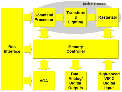
From a high-level you can see that the P10 isn't very different at all. The biggest improvement over the competition here is the use of a 256-bit DDR memory bus. The GeForce4 and Radeon 8500 both use a 128-bit DDR memory bus so this effectively doubles the peak theoretical memory bandwidth that can be attained. Because of the use of BGA memory it becomes easier to route traces making 256-bit DDR memory buses a reality for more than just 3DLabs, they're simply the first to introduce it. While 3DLabs hasn't released any card specs yet, they are claiming over 20GB/s of memory bandwidth is possible with the P10 meaning that they'd need at least 312.5MHz DDR SDRAM. Considering that the current GeForce4 Ti 4600 uses 325MHz DDR SDRAM, it's very possible that you'll see cards with over 20GB/s of memory bandwidth.
Other than the 256-bit memory bus and the addition of a block labeled as the Command Processor (which we'll get to later), the P10 looks pretty familiar; here are some quick specs:
- 0.15-micron manufacturing process (same process as the GeForce4)
- 76M transistors
- Fabbed at TSMC (NVIDIA's chips are made here as well)
- 860 ball HSBGA package (TSMC's latest packaging technology)
- 4 pixel rendering pipelines, can process two textures per pipeline
- 256-bit DDR memory interface (up to 20GB/s of memory bandwidth w/ 312.5MHz DDR)
- up to 256MB of memory on-board
- AGP 4X support
- Full DX8 pixel and vertex shader support
We've been deliberately light on the specs here as the rest must be explained in greater detail; it wouldn't do them justice to put them in a simple list.
The 3D Pipeline
We've already said that the P10 pipeline isn't really any different from a conventional 3D pipeline, but what defines a "conventional" 3D pipeline? Let's just take a brief tour of how the 3D pipeline works:
1) The first stage is the most obvious, sending commands and data to be executed on the graphics chip. This is initiated by the software running on the host CPU, sent over the AGP bus and finally reaching the graphics processor which is contacted using the graphics drivers.
2) Now that the GPU knows what data it needs to begin processing and what it needs to actually do to this set of data, it starts working. The data sent to the GPU is sent in the form of the vertices of the polygons that will eventually be displayed on your screen. The first actual execution stage in the graphics pipeline is what has been referred to as T&L for the longest time. This is the transformation of the vertex data that was just sent to the GPU into a 3D scene. The transformation stage requires a lot of highly repetitive floating-point matrix math. Next comes the actual lighting calculations for each of these vertices. In a programmable GPU these initial vertex processing stages are very flexible in that short vertex shader programs can be written to control a number of the characteristics of the vertices to change the shape, look or behavior of a model among other things (e.g. matrix palette skinning, realistic fur, etc..).
3) After we have beautifully transformed and lit vertices it's time to actually generate some pixels so they can be displayed on your screen. But before that there's a bit of house keeping to be done. There are the culling and clipping stages that basically remove all the vertices that extend beyond the bounds of the scene. Then we have some of the nifty visibility calculations that go on in most of today's GPUs to help throw out vertices that won't be visible to the user. This is where technologies such as HyperZ and NVIDIA's Visibility Subsystem come into play to throw out data before we actually start rendering pixels and waste fill-rate and memory bandwidth.
4) Now that we've had our spring cleaning it's time to generate some pixels. The remaining vertex data now converted into viewport space which is the 2D space of your monitor; remember that although this is 3D rendering, you're still looking at a flat (2D) monitor. The z-buffer data (how far away/deep the pixels are in reference to the viewer) is calculated and stored as well in order to turn this otherwise 2D image into a 3D world.
5) Texture coordinates are calculated which will be used to map textures onto these polygons that have been created using the vertex data. The textures are then loaded and then we have the pixel shading stage where today's programmable GPUs can allow small programs to run and create neat looking effects on the pixels (e.g. shadow mapping, z-correct bump mapping, etc…).
6) Finally we've come to the end of the pipeline where all final filtering, anti-aliasing, and other such techniques take place before the final pixel data is stored in the frame buffer and sent out to the RAMDAC or TMDS transmitter(s).
Now it's important to realize that this pipeline is the same for the P10 as it is for the GeForce4. What's different is determined by what happens within those stages.

The 3DLabs P10 VPU Pipeline - Click to Enlarge
(Note: Yellow blocks are programmable, orange are fixed function)
Above we have an overview of the P10's 3D pipeline, if you want to follow along as we touch on the different areas you can keep the enlarged image open in another window; it may help you understand the technology a bit better.
Multithreaded Graphics?
When dealing with multiple 3D threads being sent to the graphics card there are a number of things that must be taken into account that aren't normally considered. Management of execution resources, context switching time and the ability to dedicate resources to certain tasks are all examples of problems that arise.
For starters, this would almost never happen in any of today's games. In order to see the applications for this sort of parallelism you'd have to look at the professional world and even to the future of Microsoft OSes. If you haven't heard the codename Longhorn before then let us provide you with a short introduction. Longhorn is the codename for Microsoft's next-generation UI for Windows that promises to make extensive use of hardware DirectX acceleration of the desktop. When simply working with Longhorn you'll immediately have a number of different threads being sent to your graphics card, and managing them can become an issue.
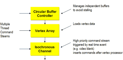
3DLabs is particularly proud of their command processor which is designed to handle these multithreaded situations. Whenever you're dealing with multiple threads being executed in parallel you want to make sure that you're maximizing your execution resources; this is one of the major roles of the command processor. The command processor offers per-thread command buffers which is a feature that has been around in high-end cards for a while. In the event that one thread sends corrupt data to the video card the thread will die but the OS will continue to function which is very important for situations like under Longhorn. In a present-day situation, if a game sent corrupt data to your video card then you'd get a lovely bluescreen without per-thread command buffers to provide some insulation from concurrent threads. The command processor also allows for extremely quick state changes which comes in handy when you are switching between multiple 3D windows.
From the standpoint of making a great deal of sense for Longhorn, these are all great features to have but they won't be tangible for most users for quite some time. The command processor does play an active role in any multithreaded 3D application where the VPU is being requested by multiple threads. For current games, the command processor isn't nearly as important as the other features of the part but it's worth mentioning nonetheless.
16 FP Vertex Processors
In stage 2 we talked about the transformation and lighting of vertices and the role vertex shaders play in today's programmable GPUs. By far the most powerful desktop GPU when it comes to vertex shaders is NVIDIA's GeForce4 which has two vertex shaders. The 3DLabs P10 on the other hand has 16 32-bit floating-point geometry processors that handle vertex processing, does this mean that the P10 has 8 times the vertex throughput of the GeForce4? Of course not, let's start off by making this an apples to apples comparison.
Each one of NVIDIA's vertex shader units operates on 4 element vector data (vect4) which is perfect for the type of work these units have to perform. Unfortunately if you send anything other than a vect4 operand to the vertex processor you'll lose efficiency. For example, these units can only handle one scalar at a time; if you recall from our explanation of the 3D pipeline, the transformation process makes heavy use of matrix math and the generation of scalar values occurs quite frequently here. Even with dual vertex shader units, the loss of efficiency when dealing with anything other than a vect4 operation is significant. For example, a vect4 operation can be processed in a single clock cycle through NVIDIA's vertex shader unit but it takes the same amount of time to process a single scalar operation. ATI's vertex shaders are setup in the same way and if you were to convert ATI/NVIDIA vertex shaders to what 3DLabs is referring to when they use the term "Vertex Processor" you could claim that each one of their units has 4 vertex processors.
The P10 uses a different approach; instead of using very powerful units, 3DLabs went to a more granular setup where they have a total of 16 32-bit scalar vertex processors (VPs). Each one of these processors can crank out a scalar operation in one clock cycle, but they take four clock cycles to complete a vect4 operation. The reason the P10 has the potential to be faster at all types of vertex operations is because there are so many (16) of these VPs in parallel.
If you are comparing theoretical vertex throughput between the P10 and the GeForce4's dual vertex shaders you'd end up with a little more than a 2x advantage in favor of the P10. The reason for the potential advantage being a more than 2x is because of the gain in efficiency when dealing with scalar operations that can be completed in one clock cycle through any of the 16 VPs in parallel.
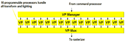
Software only sees one virtual VP and interacts with the VP manager which then
takes on the role of managing all 16 VPs.
From a software standpoint, the massively parallel array of VPs goes completely unnoticed. The developer can treat the array as a single vertex processor, a VP manager properly assigns and distributes the operations among the 16 parallel VPs. In the end a multiplexer chooses from the VP outputs and sends the data to the next stage of the pipeline.
This array of 16 VPs is the P10's version of NVIDIA's vertex shaders and they do offer full support for all current DX8 vertex shaders. 3DLabs believes that they will be able to claim full support for the Vertex Shader 2.0 specification in DirectX 9 but given that DX9 isn't out they cannot officially claim support yet.
Not a Tile-Based Architecture
While the P10 is thankfully devoid of most horrible marketing names, the one name they did use was done pretty poorly. In the rasterization to viewport space stage (4) the P10 uses what 3DLabs calls the Tile Processor. The tile processor does split up the rendering of the scene into tiles but that does not make the P10 a deferred rendering architecture.
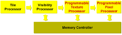
Instead, the P10 divides the scene up into 8x8 blocks of pixels and processes the scene in that matter. This method of was chosen simply because it makes the most efficient use of the P10's caches. 3DLabs has done internal simulation to illustrate this and the method in which the P10 renders is best optimized for their architecture. In the end the main thing to take away from this is that the P10 is an immediate-mode renderer just like the GeForce4 or Radeon 8500.
3DLabs has outfitted the P10 with what they call a visibility processor that performs the z-occlusion culling in the pipeline. We didn't get much information on the visibility processor but it's safe to assume that the feature set is comparable to what we've seen from ATI and NVIDIA.
The P10's "Pixel Shaders"
One of the biggest rocks that 3DLabs is throwing at the ATI/NVIDIA camp is calling their "pixel shaders" not truly programmable. Instead, 3DLabs consistently refers to ATI/NVIDIA pixel shaders as register combiners that allow flexibility but aren't truly programmable. This goes back to the Carmack quote from earlier expressing displeasure with the way NVIDIA's pixel shaders turned out.
3DLabs doesn't discredit the power of these register combiners but they say it's not enough and thus the P10 offers a separate solution. The P10's programmable texture processor supports all current DX8 Pixel Shader specifications but, just like their vertex engine, it is composed of a number of 32-bit processors in parallel.
![]()
The P10's Four Pixel Pipelines
(Note: Yellow blocks are programmable, orange are fixed funtion)
The P10 has a total of 64 floating point coordinate generator processors that help determine texture coverage while another 64 integer processors are used to calculate the final pixel colors. As you can expect, all of these processors are fully programmable and as we just mentioned they support a superset of all currently available DX8 Pixel Shader functions.
It is important to note that although the P10 does offer a superset of all DX8 Pixel Shaders, this isn't a true DX9 part. One of the requirements for DX9 are floating-point pixel pipelines from start to finish, and as we just mentioned this simply isn't the case for the P10. Moving to floating point processors throughout the pipeline simply isn't economically viable for 3DLabs with the P10 when you take into account the increase in gates over the present mixed fp/integer setup. 3DLabs hypothesizes that they will need to be on at least a 0.13-micron process and maybe even a 0.1-micron process before full DX9 compliance will be possible. TSMC's 0.13-micron process isn't mature enough for 3DLabs to feel comfortable with from an economic standpoint, so we'll have to wait until next year for DX9 to be brought to this platform. You should also keep in mind that NVIDIA's next-generation part (NV30) will be made on TSMC's 0.13-micron process and will most likely be a full DX9 part when it comes out this fall.
In terms of other features supported by the P10's programmable texture processor, the VPU can apply 8 textures in a single pass (not a single clock) in comparison to the Radeon 8500's 6 and the GeForce4's 4. The processor also supports arbitrary texture sizes which will be important for Longhorn but again that is more of an enablement feature than something presently demanded.
Although common texture filtering algorithms are hard-wired into the pixel pipelines, the P10 also allows for custom filters to be programmed (e.g. custom anisotropic filtering shapes).
Another Programmable Stage
The final stage in the P10's pipeline is also made programmable which is something that no currently available GPU offers. After a pixel has been textured and filtered then other techniques such as anti-aliasing can kick in and do their thing. In all other GPUs these final processes are not programmable and are all hard-wired into the pipeline, but the P10 they are not.
The P10 supports virtually any type of anti-aliasing you can think of; edge anti-aliasing is supported under OpenGL which is the AA method of choice as the performance hit is significantly less than more brute force methods while offering excellent line AA quality. Supersampling and multisampling are supported as well; the former offers virtually unlimited samples while you are limited to a maximum of 8x when multisampling.
Because of the final programmable pixel stage the P10 can support much higher precision color depths such as 64-bit color. A feature you'll end up seeing more of going forward is the support for gamma-correct 10-bit RGB outputs which is built into the P10. The VPU also has 10-bit DACs to take advantage of the custom 10:10:10:2 (RGBA) mode.
Virtual Memory - Bringing L2 Cache to the VPU
Another fairly major feature that is brought to the table with the P10 is what 3DLabs calls the P10's Virtual Memory System (VMS). The way VMS works is by storing all textures in main memory and treating the memory on the graphics card itself as a very large cache. When a texture is requested, the entire texture isn't downloaded instead a 256x256 block of 32-bit pixels can be pulled in locally and accessed. The perfect example of where this would be useful is when you're walking around in a 3D environment and only a small part of a texture is visible on the screen. In traditional architectures the entire texture must be downloaded but with the P10's VMS the entire texture will remain in system memory and only the part being seen will be transferred to video memory. This may sound a lot like AGP texturing which it is, with the exception being that it is more like AGP textured but cached. The partition of system memory that is used as the P10's VMS does not need to be contiguous which is also useful.
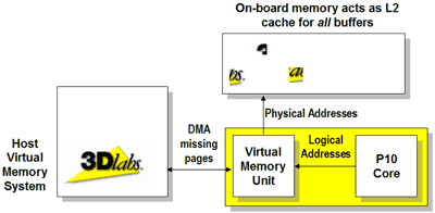
From the standpoint of game developers, VMS is quite attractive as it enables the use of far more textures than is currently possible. Currently game developers are very cautious to use more textures that there is available video memory because swapping out to main memory results in a huge performance hit. But with VMS you get the benefits of an extremely high bandwidth caching effect and can deal with much larger textures than ever before.
The best way to understand the benefits of VMS is by looking at the CPU world. Let's say that the L2 cache on your CPU wasn't really a cache but rather a small amount of high-speed memory that didn't cache system memory at all. As long as the data the CPU needed was in its on-board memory, the performance was extremely fast. However as soon as the application you were running exceeded the local memory size, the performance hit was incredible. Would it make the most sense for application developers to write all of their software so that it only fits within the 512KB of memory on your CPU itself? Or would it make more sense for CPU manufacturers to treat that small amount of memory as a cache and enable developers to use a much larger amount of memory? Obviously you'd want the latter, while things would be much faster running entirely out of high speed local memory it is not only expensive but also limits the software developers in a tremendous way.
In order to get the viewpoint of someone faced with the limitations of current memory architectures we asked Tim Sweeney of Epic Games what his thoughts were on the P10's VMS:
"This is something Carmack and I have been pushing 3D card makers to implement for a very long time. Basically it enables us to use far more textures than we currently can. You won't see immediate improvements with current games, because games always avoid using more textures than fit in video memory, otherwise you get into texture swapping and performance becomes totally unacceptable. Virtual texturing makes swapping performance acceptable, because only the blocks texels that are actually rendered are transferred to video memory, on demand.
Then video memory starts to look like a cache, and you can get away with less of it - typically you only need enough to hold the frame buffer, back buffer, and the blocks of texels that are rendered in the current scene, as opposed to all the textures in memory. So this should let IHV's include less video RAM without losing performance, and therefore faster RAM at less cost.
This does for rendering what virtual memory did for operating systems: it eliminates the hardcoded limitation on RAM (from the application's point of view.)"
Final Words
The first question you're probably asking is what market is the P10 targeted at? In spite of 3DLabs' acquisition by Creative Labs, the company will still remain an independent brand that will continue to tailor to the professional market. The P10 will be first made available very soon on a 3DLabs card aimed at the professional market. But the chip obviously has a lot of potential in the consumer/gaming market and indeed it will make its way down there.
This is where Creative Labs comes in; Creative will take the P10 technology and tailor it to the specific needs and requirements for the gaming market. The P10 will then be found on Creative Labs branded boards that will sell at prices competitive with the GeForce4 (or whatever NVIDIA's high-end card is at the time). While 3DLabs wouldn't give us an indication of exactly when we could expect consumer/gaming cards from Creative, they did say it would be before the end of the year. That could mean anything from August to something a bit closer to the holidays, although our money is on a release sooner rather than later.
In terms of the viability of the P10's architecture, it's definitely a very powerful chip. The goal of making the P10 perfect for higher level language programmability may be a bit overly optimistic for 3DLabs, at least in their first incarnation of their VPU technology. Although the vertex processors are clearly ready for this type of a role, the rest of the pipeline has to be just as flexible and capable which it presently is not. It will be interesting to see how their next-generation VPU on a 0.13/0.10-micron process turns out with a full DX9 compliant pipeline.
To the end user, the lack of full DX9 support may be a turnoff for many but keep in mind that the DX8 support the early adopters of the GeForce3 bought hasn't really been useful, even today.
As unexpected as 3DLabs' announcement was (we weren't anticipating it for another few weeks) it's just the first in a line of new technologies in the graphics sector.


