
Original Link: https://www.anandtech.com/show/886
Intel Developer Forum Spring 2002 - Wrap Up
by Anand Lal Shimpi on March 5, 2002 12:00 PM EST- Posted in
- Trade Shows
Now back in Raleigh working on our next round of server and workstation CPU reviews it's time to bring our IDF coverage to a close. During the planning stages of our IDF trip we were strongly encouraged to stay through at least the keynote on Thursday, February 28th. Because of already hectic schedules a trip to cover IDF wouldn't normally extend for that long however we were promised that Thursday's keynote by Pat Gelsinger would definitely be worth our while.
Pat Gelsinger is Intel's first CTO and an engineer at heart; what he covered in his keynote on Thursday was proof of just that. We got our dose of heavily overclocked processors earlier in the week with the liquid-cooled 4GHz Pentium 4, the future of PCs and notebooks was demonstrated and we even picked up on a few interesting things during the technology showcase. Gelsinger's focus however was on a few key areas that Intel has been working on over these past several years.
This year's Spring IDF has been the perfect example of Intel's continual departure from being just a CPU manufacturer to becoming a silicon device manufacturer. While Intel doesn't always make the most desirable CPUs for our community, they are definitely making key innovations in the future of computing. Case in point would be technology announcements such as their Bumpless Buildup Layer packaging as well as their TeraHertz SOI transistors which use a fully depleted channel vs. the partially depleted channel of AMD's SOI transistors (thus allowing for lower voltage operation with less leakage current, but then again Intel's FD-SOI is 3 years away while AMD's PD-SOI is months away).
On the last day of this year's Spring IDF Intel made some more of those technology announcements that will actually have a much bigger impact on computing in general than you might guess at face value. The time period we're living in now has always been called the Information Age with communication being a large part of our existence, improving communication both on and off chip was the focus of Gelsinger's final keynote at IDF.
BBUL in Action
When we originally brought you our article on Intel's BBUL packaging technology we had some shots of what a BBUL CPU would look like. During his keynote, Gelsinger provided another FC-PGA vs. BBUL demonstration which will hopefully give you a refresher of the benefits of BBUL.
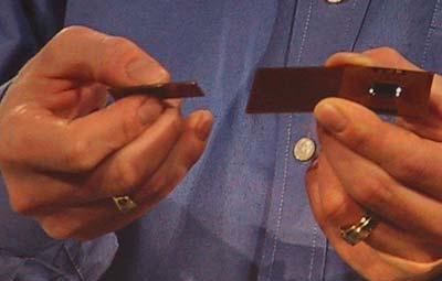
The surface of the package is completely flat which will make cooling an easier task and of course there are the other advantages which we illustrated in our original article. While we won't get into them here, we'll provide an abridged list as a refresher:
- Enables much greater micro-via counts
- No solder bumps
- Enables cost-effective multi-core CPUs and multi-chip packages
If you're tired of waiting for Serial ATA to happen then you probably shouldn't have read about BBUL as it'll take another 5 years for this technology to be implemented in CPUs. As usual, it'll start where needed the most and in low-volume areas and then move on to the mainstream and eventually BBUL will be used on all Intel CPUs.
Wireless Everything
A proposal that Gelsinger made at IDF was to eventually introduce what he called a "Radio Free Intel." The term is a bit of a misnomer as Intel is planning on providing Radio Frequency (RF) technology free on future silicon devices.
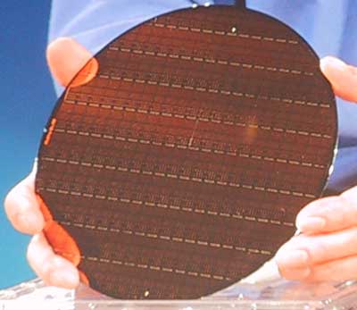
A MEMS wafer
Intel has been experimenting quite a bit with what are known as Micro-electro Mechanical System (MEMS) devices which are essentially devices that rely on the physical properties of the silicon they're built on to mimic mechanical devices that exist today. Examples would be levers, capacitors, inductors, etc... all implemented in silicon through the use of these MEMS devices.

The benefit Gelsinger was quick to point out was the size reduction of RF transmitters and receivers. Currently if you look at any RF device you'll note that the vast majority of the device consists of analog components capacitors, inductors, etc... and only a few pieces of silicon are rarely ever found on board.
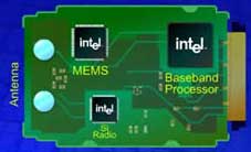
Intel's goal, moving forward, is to integrate as many of these components as possible into silicon through the use of MEMS devices. Thus producing a much smaller form factor board, and eventually reducing the size of the device into a small piece of silicon that can be integrated into chipsets and CPUs.
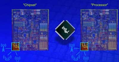
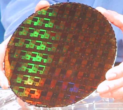
Most of the components required for RF circuitry have already been implemented in Silicon as Intel attempted to demonstrate with this Si-Radio wafer.
The possibilities for this will be endless. It'll still be a few years before we start seeing Intel CPUs and chipsets ship with integrated Silicon Radio technology but when they do it will mean that wireless connectivity is no longer something you'll have to think about, it will just be there. Rumor has it that Banias will begin to implement some of these technologies but it's unclear at what level or what we should expect. One thing is for sure, wireless network access will be a major part of Banias and future Intel CPUs going forward.
Other capabilities such as the ability to seamlessly transition from one network to another and even across different types (LAN to wireless LAN to wireless WAN, etc...) must be enabled as well which will also the delay the introduction of this technology. Then there are security issues and IP addressing issues that must be worked out, having an RF transmitter in your CPU wouldn't be too useful if you couldn't roam beyond an access point giving you an IP address. The ability to join networks anywhere and always remaining connected to the Internet is a major focus of this technology.
Silicon Photonics
While this is a bit out of the realm of our normal discussion, part of Gelsinger's speech was about Silicon Photonics - the modulation of data onto wavelengths of light. The future of this technology is very bright (no pun intended) because it could eventually be brought down to the chip level where datapaths within the CPU are made out of optical connections using multiple wavelengths of light to send tremendous amounts of data.
Of course no mention of forward-looking technology would be complete
without a silicon wafer shot; this one above is a wafer of some of Intel's Si-Photonics
devices and doesn't actually implement any light datapaths on chip as that's
quite a while away.
Final Words
This concludes our coverage of the Spring 2002 Intel Developer Forum which has undoubtedly been the most interesting conference over these past several months. If you haven't kept up with all of our coverage be sure to go back and read the earlier IDF articles since the technology we've been talking about will surely pop up in future discussions as it matures.
- Intel Developer Forum Spring 2002 - Day 1
- AMD's Hammer in Action: The most impressive demo of IDF
- Intel Developer Forum Spring 2002 - Day 2
- Intel Developer Forum Spring 2002 - Day 3
- Intel Developer Forum Spring 2002 - Day 4
We hope you enjoyed our coverage and now it's back to the normal product reviews.


