Original Link: https://www.anandtech.com/show/8814/intel-releases-broadwell-u-new-skus-up-to-48-eus-and-iris-6100
Intel Releases Broadwell-U: New SKUs, up to 48 EUs and Iris 6100
by Ian Cutress on January 5, 2015 10:00 AM EST
As part of the CES cavalcade of announcements, after launching Core-M back in September, Intel is formally releasing their next element of the 14 nanometer story: Broadwell-U. As the iterative naming over Haswell-U suggests, Broadwell-U will focus on dual-core 15W and 28W units from Celeron to Core i7 using 12 to 48 execution units for the integrated graphics. A Broadwell-U processor should drop into any existing Haswell-U equivalent design (i3 to i3) due to pin and architecture compatibility, albeit with a firmware update.
As with any node change, the reduction to 14nm affords the usual benefits: more transistors per unit area, lower power consumption for a given design, or the potential to increase performance. Ryan covered the details of Intel’s 14nm architecture back as part of the IDF launch, as well as a good deal of the Broadwell architecture itself. The launch today is in essence a specification list with a few extra details, along with potential release dates for Broadwell-U products. The CPUs are already shipping to partners for their designs.
There will be several combinations possible throughout the Broadwell line, but the most important distinctions are:
28W with GT3, Iris 6100 Graphics (48 Execution Units)
15W with GT3, HD 6000 Graphics (48 Execution Units)
15W with GT2, HD 5500 Graphics (23 Execution Units for low i3, 24 for others)
15W with GT1, HD (Broadwell) Graphics (12 Execution Units)
The graphics move up to Generation 8, and a lot of architectural detail into this was given by Intel and IDF San Francisco in September 2014 of which some of the important points are highlighted here.
The New SKUs
Without further delay, the list of the new processors is as follows:
| CPU | Cores | Base Freq (GHz) | 1C (GHz) | 2C (Ghz) | EUs | GPU Base / Max Freq (GHz) |
LPDDR3 / DDR3 Support (MHz) |
L3 Cache | cTDP Down | vPro | 1K $ |
| Intel Broadwell-U 28W + Iris 6100 Graphics |
|||||||||||
| Core i7-5557U | 2 / 4 | 3.1 | 3.4 | 3.4 | 48 | 300/1100 | 1866/1600 | 4MB | 23W | No | $426 |
| Core i5-5287U | 2 / 4 | 2.9 | 3.3 | 3.3 | 48 | 300/1100 | 1866/1600 | 3MB | 23W | No | $315 |
| Core i5-5257U | 2 / 4 | 2.7 | 3.1 | 3.1 | 48 | 300/1050 | 1866/1600 | 3MB | 23W | No | $315 |
| Core i3-5157U | 2 / 4 | 2.5 | 2.5 | 2.5 | 48 | 300/1000 | 1866/1600 | 3MB | 23W | No | $315 |
| Intel Broadwell-U 15W + HD 6000 Graphics |
|||||||||||
| Core i7-5650U | 2 / 4 | 2.2 | 3.2 | 3.1 | 48 | 300/1000 | 1866/1600 | 4MB | 9.5W | Yes | $426 |
| Core i7-5550U | 2 / 4 | 2.0 | 3.0 | 2.9 | 48 | 300/1000 | 1866/1600 | 4MB | 9.5W | No | $426 |
| Core i5-5350U | 2 / 4 | 1.8 | 2.9 | 2.7 | 48 | 300/1000 | 1866/1600 | 3MB | 9.5W | Yes | $315 |
| Core i5-5250U | 2 / 4 | 1.6 | 2.7 | 2.5 | 48 | 300/950 | 1866/1600 | 3MB | 9.5W | No | $315 |
| Intel Broadwell-U 15W + HD 5500 Graphics |
|||||||||||
| Core i7-5600U | 2 / 4 | 2.6 | 3.2 | 3.1 | 24 | 300/950 | 1600/1600 | 4MB | 7.5W | Yes | $393 |
| Core i7-5500U | 2 / 4 | 2.4 | 3.0 | 2.9 | 24 | 300/950 | 1600/1600 | 4MB | 7.5W | No | $393 |
| Core i5-5300U | 2 / 4 | 2.3 | 2.9 | 2.7 | 24 | 300/900 | 1600/1600 | 3MB | 7.5W | Yes | $281 |
| Core i5-5200U | 2 / 4 | 2.2 | 2.7 | 2.5 | 24 | 300/900 | 1600/1600 | 3MB | 7.5W | No | $281 |
| Core i3-5010U | 2 / 4 | 2.1 | 2.1 | 2.1 | 23 | 300/900 | 1600/1600 | 3MB | 10W | No | $281 |
| Core i3-5005U | 2 / 4 | 2.0 | 2.0 | 2.0 | 23 | 300/850 | 1600/1600 | 3MB | 10W | No | $275 |
| Intel Broadwell-U 15W + HD (Broadwell) |
|||||||||||
| Pentium 3805U | 2 / 2 | 1.9 | 1.9 | 1.9 | 12 | 100/800 | 1600/1600 | 2MB | 10W | No | $161 |
| Celeron 3755U | 2 / 2 | 1.7 | 1.7 | 1.7 | 12 | 100/800 | 1600/1600 | 2MB | 10W | No | $107 |
| Celeron 3205U | 2 / 2 | 1.5 | 1.5 | 1.5 | 12 | 100/800 | 1600/1600 | 2MB | 10W | No | $107 |
There are some clear patterns in the product line. Every unit apart from the Pentium and Celerons has hyperthreading, putting most of the line in a dual core, quad thread scenario. This also ties in with the Pentium and Celeron’s use of HD (Broadwell) graphics, which is a 24 EU design with half of each subslice disabled. The speeds of the Pentium and Celerons are also cut back, despite the 15W TDP and high cTDP down, ensuring that these are the bargain basement units of the line.
vPro will only be enabled on i7-56x0U and i5-53x0U series, giving a range if HD 6000 or HD 5500 is needed, however there is no vPro Iris 6100 part being released. The HD 5500 parts will have a cTDP Down of half their original TDP, allowing 7.5W designs to also take advantage of Broadwell-U.
The Core i3 15W SKUs have an odd combination involving 23 EUs rather than the 24 EUs that the die is designed with, presumably in order to keep yields higher it gives Intel a chance to still sell those with a single defect. This produces a lop-sided EU design within the configuration, which has its own implications, and we are requesting more detail from Intel as to how this is managed in the firmware.
A positive point for 6x00 series graphics SKUs is the memory compatibility on LPDDR3, with these units (having an 5 or an 8 in the 00x0 name) allowing 1866 MHz memory. As our previous Haswell desktop memory testing has shown a small bump away from 1600 MHz DRAM can give a good performance boost when it comes to graphics, especially when the memory speed between CPU and DRAM is the main bottleneck. I would be interested in exploring the difference with this for sure.
It might come across as somewhat surprising that a 15W CPU like the i7-5650U has a 2.2 GHz base frequency but then a 3.2 GHz to 3.1 GHz operating window, and yet the i7-5557U has a 3.1 GHz base with 3.4 GHz operating for almost double the TDP. Apart from the slight increase in CPU and GPU frequency, it is hard to account for such a jump without point at the i7-5650U and saying that ultimately it is the more efficient bin of the CPUs. So while the 28W models will get the glory in terms of performance, there are a number of models that can offer just under that performance but for just over half the power rating. This obviously levels battery life for the more efficient design as a significant jump, depending on how the system as a whole is used.
The Dies and Packaging
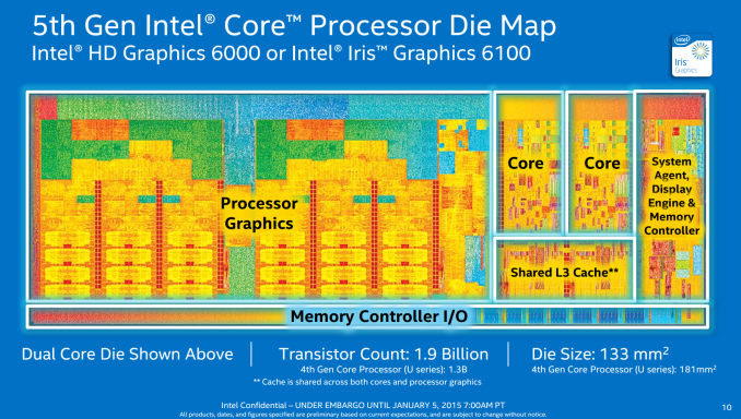
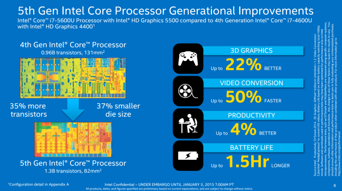
Broadwell-U will be derived from two main dies. The larger design contains the full 48 EU (two common slices with 6x8 EU sub-slices all in) configuration for 1.9 billion transistors in 133 mm2, while the 24 EU design (one common slice, 3x8 sub-slices) will measure 1.3 billion transistors in 82 mm2.
This puts the size of one common slice with 3x8 sub-slices at 600 million transistors / 49 mm2, and thus the die without the graphics subsystem at all at 700 million transistors for 33 mm2. This would mean the cores, the Last Level Cache, the IO and memory controller all fit into the 700 million.
Compared to Haswell-U, Intel provided the following data:
Broadwell-U with HD 5500 (24 EU) has 240M more transistors than Haswell-U with HD 4400 (20 EU)
Broadwell-U with HD 6000 (48 EU) has 600M more transistors than Haswell-U with HD 5000 (40 EU)
Unfortunately calculating the increases for separate parts is a little more difficult than just comparing numbers due to the different elements of the new graphics, known as Intel Gen 8.
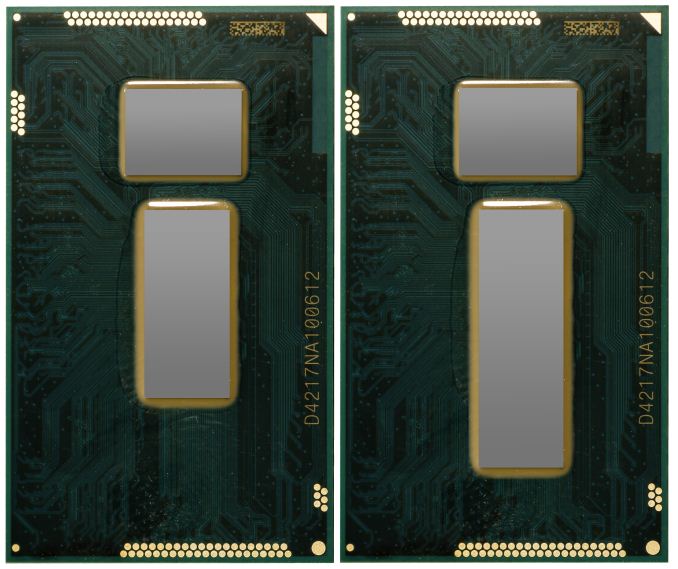
In terms of the packaging for the dies, we also have some shots of those to share:
On the left is the 2+2 configuration, giving two cores and GT2 (24 EUs), while on the right is the 2+3 package. The silicon on top is the Platform Controller Hub, discussed later.
Broadwell GPU Improvements
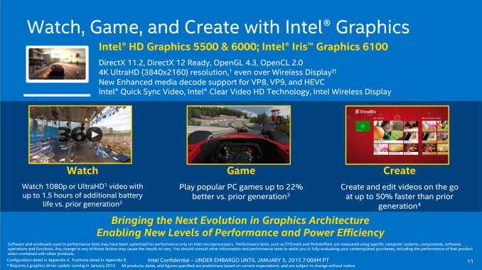
The new integrated graphics for Broadwell from Intel in the form of HD 5500, HD 6000 and Iris 6100 open up some very important functionality. DirectX 11.2, OpenGL 4.3 and OpenCL 2.0 are big scoring points, especially OpenCL 2.0 when it comes to graphics compute. This includes features such as shared memory coherency between CPU and GPU to allow transfer of pointer-rich memory structures and ultimately the beginnings of heterogeneous CPU + GPU compute.
‘DirectX 12 Ready’ is somewhat of an interesting case, and it depends on Microsoft’s final specifications. At this point in time Intel state that they conform to as much of DirectX 12 feature set that they can get their hands on with their relationship with Microsoft, and barring any major addition or change, should be compatible. UHD-4K is also now supported through the HDMI 1.4b interface, albeit limited to 24 Hz.
Support for HEVC is also present in terms of a combined (hybrid) hardware and software solution, just as it was on Core-M. Intel stated that as parts of the H.264 algorithm are near if not identical to those of the H.265, with a small tweak to the hardware it can be used for both. This is still not an all-encompassing hardware acceleration, but it does aim at some parts of the codec. I would speculate that if a full section of the silicon could be made for complete hardware acceleration, it might eat into certain power budgets.
GPU Slices
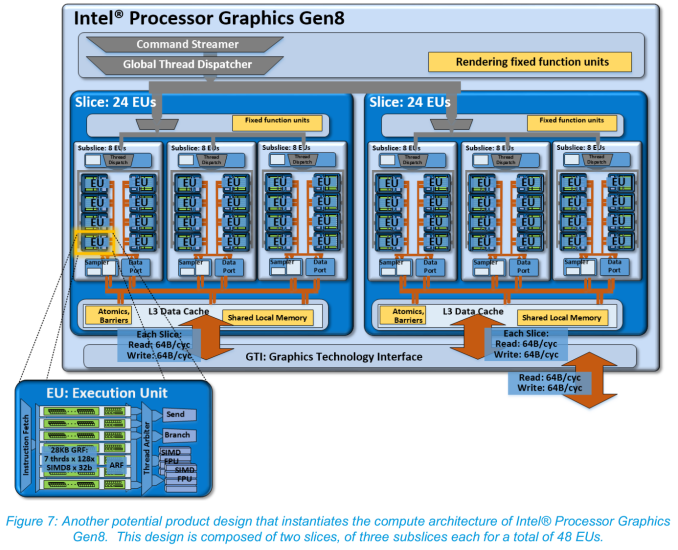
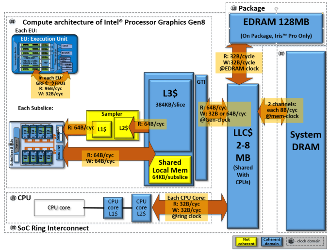
Although mentioned in our Broadwell architecture overview, for Broadwell-U we should cover the basics of the GPU layout. Below is an image of a HD 6000 implementation featuring two slices of 24 EUs each, with each slice having three sub-slices of 8 EUs. Each EU can handle 7 threads at once when in a 128xSIMD8 32-bit configuration. When in the right data structure, this offers a good amount of power, especially to coalesced 16-bit computation.
For Broadwell, Intel has reduced the number of EUs in a sub-slice from 10 down to 8. This is a big change, as it eases up the Thread Dispatch, Data Port and L1/L2 samplers in each EU as they have to deal with less data overall. By this logic, with two equivalent designs, one with 8 EUs per sub-slice should be able to get through more data due to less data bandwidth pressure and less competition for each sub-slice’s shared local memory.
Each slice has an L3 Data Cache, which for Gen8 is improved from 384 KB to 576 KB per slice. This ends up being split anyway as 64 KB per sub-slice as shared local memory and 384 KB for inter-slice L3 communication. More slices mean more caching overall, and as an aid to the last level cache outside the GPU, the Graphics Technology Interface has doubled the write bandwidth.
The principle behind caches is to provide a small amount of memory that can be accessed faster at the expense of size. The algorithms in place to predict which data is needed next (or preprogrammed data fetching) helps increase the overall speed of any CPU function, but increasing the size of a cache decreases the need for later caches by reducing the data misses that require trips further out. GPUs are historically bandwidth starved, both for gaming and for compute, so by virtue of having four named caches for the GPU to use and increasing at least the third, this should contribute to the large performance numbers Intel is producing in comparison to the previous generation.
In terms of throughput, Intel gives the following numbers for GT2 / 24 EU configurations:
32b FP: 384 FLOP/cycle = 24 EUs * (2 * SIMD-4 FPU) * (MUL + ADD)
64b DP: 96 FLOP/cycle = 24 EU * SIMD-4 FPU * (MUL + ADD) * 0.5 throughput
32b INT: 192 IOP/cycle = 24 EU * (2 * SIMD-4 FPU) * ADD
The Gen8 EUs will support 16-bit floats (half-floats) natively, as well as 16-bit integers.
We can construct a table calculating out to full performance:
| Intel Gen8 Graphics Throughput | |||
| Processor | 32b FP GFLOPs |
64b DP GFLOPS |
32b INT GFLOPs |
| i7-5557U (48 EUs at 1100 MHz) | 844.8 | 211.2 | 422.4 |
| i5-5257U (48 EUs at 1050 MHz) | 806.4 | 201.6 | 403.2 |
| i3-5157U (48 EUs at 1000 MHz) | 768 | 192 | 384 |
| i7-5250U (48 EUs at 950 MHz) | 729.6 | 182.4 | 364.8 |
| i7-5600U (24 EUs at 950 MHz) | 364.8 | 91.2 | 182.4 |
| i5-5300U (24 EUs a 900 MHz) | 345.6 | 86.4 | 172.8 |
| i3-5010U (23 EUs at 900 MHz) | 331.2 | 82.8 | 165.6 |
| i3-5005U (23 EUs at 850 MHz) | 312.8 | 78.2 | 156.4 |
| Pentium 3805U (12 EUs at 800 MHz) | 153.6 | 38.4 | 76.8 |
Having doubled the EUs not only doubles the performance but the extra bit of frequency also helps.
As we mentioned back in August, the sub-slice also gets some minor improvements to increase pixel and Z-fill rates, and the front end’s geometry units are also beefed up. Further reading can be found on Intel’s PDF on the Gen 8 Graphics Overview from IDF.
Fitting in With Core M
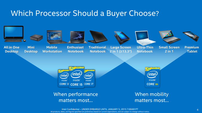
The staggered release of Broadwell is nothing new. Previous releases from Intel has seen them pick a particular market and aim at that first, whether it be tablet, mobile devices, ultrabooks or desktops, with the rest to follow. Core M, Intel’s 4.5 W ‘Broadwell-Y’ part, has been in the market for over a month with designs such as the Lenovo Yoga 3 Pro, although the number of SKUs available as well as worldwide distribution has been relatively slow, with the designs featuring Core M being expensive in terms of casual computing and more premium upgrades. Broadwell-U changes this by opening up the power envelope, and as such Intel sees the market at follows:
The Broadwell-U processors from Intel are aiming to give enough performance from AIO desktop systems to mini desktops, premium mobile applications all through to large 2-in-1s. There is some overlap with Core M, particularly with the 7.5W cTDP down elements of the range, but the interesting element will be pricing. The Celerons come in around $100, with the Pentium at $160, but then it gets expensive for Broadwell-U. $275 to $315 covers all the i3 and i5 parts both at 15W and 28W, ending with $393/$426 for the i7 parts. Further to my efficiency comments above, on paper at least the i5-5350U or i5-5250U would seem the most interesting processors of the bunch.
Release Dates
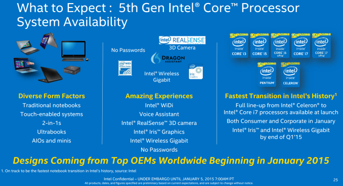
In our conference call with Intel, it was clear that these CPUs are shipping to their partners today. Throughout CES there will be a number of manufacturers announcing their products, and as per the norm Intel allows the partners to introduce their own products, rather than showing examples of where Broadwell-U fits in. However, because Broadwell-U is designed to be pin-compatible with Haswell-U, we might see some manufacturers purely re-releasing some of their designs with the newer CPU and a firmware update. Nevertheless, Intel is expecting OEM systems with Broadwell-U to start shipping in North America within the month. Designs with Iris graphics, or those featuring Intel based WiGig connectivity, will be more towards the end of Q1. Overall Intel is tracking ‘hundreds of designs’ involving Broadwell, indicating that it will be a significant push to bring 14nm to the market.
Broadwell-U: On Performance
As part of the Broadwell-U launch, it would not be complete without a list of performance related metrics direct from Intel indicating how Broadwell-U improves over Haswell-U. Without hardware on hand to test for ourselves it is hard to verify the numbers, but it provides a number of interesting talking points and how they compare to the previous Intel presentations leading up to this.
Core Improvements
We covered the transistor numbers on the previous page, but Intel’s direct performance metrics are most important when we consider graphics and battery life. Moving from Haswell-U to Broadwell-U, in terms of productivity, will not be that much of a jump as it is a similar architecture but on a different process node. It allows Intel to catch the low hanging fruit and move the IPC up by around 5%, achieved by the following:
Larger OoO scheduler
Faster store-to-load forwarding
Larger (+50%) L2 transaction lookaside buffer (TLB)
New dedicated 1GB page mode for L2 TLB
2nd TLB page miss handler
Faster FP multiplier
Faster Radix-1024 divider
Improved address prediction for branches and returns
Targeted cryptography instruction acceleration
The node adjustment has more weight when it comes to power saving, resulting in a lower voltage required for similar performance, but combined with Intel’s 2:1 policy for Broadwell (+2% performance uses at most +1% power) is good all around.
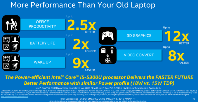
However the bigger change is on the GPU side. Intel is quoting a +22% synthetic graphics improvement from HD 5500 to HD 4400 with 3DMark and +50% for Cyberlink MediaEspresso for video conversion.
One might consider that Intel should bring alternating CPU and GPU performance each U series cycle, to give each platform a serious talking point. Haswell gave a half-generation increment in the name scheme after all (Gen7 to Gen7.5) but the CPU architecture was new compared to Ivy Bridge.
Intel is also a fan at looking into historical improvements. If you consider that a number of users are upgrading a 2-4 year old system, this makes a good amount of sense to see where the multi-generation improvements add up. On the other hand, when a person does upgrade, you would hope that every area has been improved over the 2-3 generations in the interim.
Naturally in order to give the best comparison data we look back at the oldest reasonable product for comparison – in this case Intel pitted an i5-5300U (HD 5500, GT2 with 24 EUs) against an i5-520UM. In the time between these two platforms, the concept of attacking mobile devices has changed significantly because of the base performance. If we put the 4.5W equivalent of the i5-520UM into a fanless tablet for example, the quality and features we know today would (I assume) feel slow almost to a point of excruciating. One argument is that back then, in 2010-ish (and before), our concept of software features and gaming was not at the level of detail it is today (which is true) and the same comparison will most likely be made in four years looking back at this era. Not only does the hardware improve, but also the understanding of the market and the concept of user experience.
Nevertheless, now we have devices that wake from sleep in fractions of a second rather than seconds, or turn on in seconds rather than minutes. Battery life has improved because integrated graphics are a bigger portion of the equation and we have thrown the graphics card away for most devices that need a sense of mobility. My old 8lb brick of a mobile 15-inch 1200p workstation used a 45W GPU with a 35W CPU, which was a nightmare for working on-the-go. The 11-inch netbook wasn’t a lot better, with the low 1366x768 resolution and underwhelming performance. As I am writing this review, my sub-3lb UX301 laptop is in a low power mode and on this flight I have managed three hours of active writing time, looking at text on white backgrounds, and still have half of the battery remaining. At this point four years ago, I would be getting out my charger for my 8lb brick with its extended battery and then wondering if I have exceeded the power limit for the flight socket. A popular feeling is to look back fondly to the past, but when it comes to the combination of laptop battery life with performance, the only way is forward.
Battery Life and the Audio DSP
Almost all the Intel suggested use scenarios, outside static All-In-Ones and mini-desktops, rely on some form of battery, so it makes sense that power efficiency is one card in play for Broadwell-U. In the past this relates in terms of actual performance per watt but also in regards to time-to-sleep, especially when parts of the system can be put into a lower power state or shut off completely when not in use. This makes designs complicated with disconnected clock domains as introduced in previous designs and so forth.
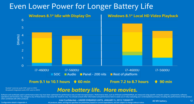
The test for battery life is also important as well because users typically do not run blank screens at idle when performing daily tasks. The two metrics Intel has provided is a 100 nit display idle with Windows 8.1, with the other requiring local HD video playback.
For the former, Intel is quoting +60 minutes of battery life on their test platform at idle, equivalent to +11.0%. Most of this power saving comes from the SoC using better power saving techniques, but also the rest of the platform, such as the PCH, also reduces its power use to around half.
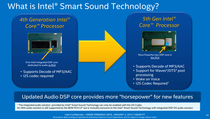
During the (local) video playback, a 90 minute difference equates to a substantial +20.8% battery use gain. A small amount of this is from the SoC and platform, but the biggest saving by far is the audio. Broadwell-Y and Broadwell-U both integrate Intel’s audio DSP (Digital Signal Processor) into the PCH. This removes a couple of Realtek components from the motherboard and allows Intel to bring it under their own manufacturing process, as well as configure the power gating needed.
The DSP is more powerful, presumably equating to a good race-to-sleep performance as well as dealing with HD audio under a lower power budget. Interestingly enough I would point out that the power usage of the DSP will be directly related to how much data is flowing through. If a HD video with little to no audio is involved, then the power usage will be quite low anyway. I would like to perhaps put a SYL metal live-show DVD through its paces to see how this affects power consumption.
As we mentioned back during the Core M discussions, the audio DSP lends itself to being a configurable and programmable entity, much in the same way that AMD’s solution is actively promoted. Similar to the response we had back then, Intel is considering opening it up with a public SDK, although that side of the equation is not on the roadmap as of yet.
Broadwell-U Platform Controller Hub (PCH)
As a writer, my bread and butter at AnandTech these past four years has revolved around motherboards and thus examining the connectivity provided by a chipset is always interesting. Because Intel bundle both the processor and the PCH on the same package, it allows manufacturers to save space in their design but it also allows Intel to control power consumption tighter to give better performance or longer battery life as a whole. There is still room for manufacturers to differentiate in their IO offerings, which is a good thing for consumers.
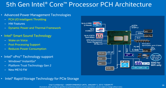
The new PCH for Broadwell-U focuses on that power consumption, especially when it comes to throttling sections and data pathways when not in use. The ‘Dynamic Power and Thermal Framework’ entry for the 5th Gen PCH should allow the performance to either respond as a function of battery life or skin temperature. This means throttling where necessary to reduce temperature or increase battery life. Wake on Voice is also a target for Intel, allowing devices to maintain a super-low power state but still respond without direct touch.
When it comes to direct connectivity, the PCH offers four SATA 6 Gbps, four USB 3.0 (two of which are muxed similar to a hub), eight USB 2.0 ports, TPM, a PCIe 2.0 x4 and another 12 PCIe 2.0 lanes split into 6 ports, allowing six devices maximum. We asked Intel regarding PCIe storage support for RST, and were told that with additional hardware support (remapping logic), Broadwell-U can support one PCIe 2.0 x2 PCIe storage device. This means that if a PCIe storage device based Broadwell-U came to market, with RST capabilities, it would cost a bit more than the base model. Also worth noting is that Broadwell-U is still using PCIe 2.0. On the PCH side this is perhaps not so much a big deal, and when asked about PCIe 3.0 Intel reiterated their stance on not commenting on possible future plans but they are monitoring demands and industry trends.
On the DRAM front, we got confirmation that Broadwell-U will support a maximum of 16GB of DDR3L/DDR3L-RS or LPDDR3 memory. No comment was made on a move towards two modules per channel memory or DDR4. Regarding video connectivity, Broadwell-U was too early for HDMI 2.0 and thus has HDMI 1.4b.
WiDi 5.1
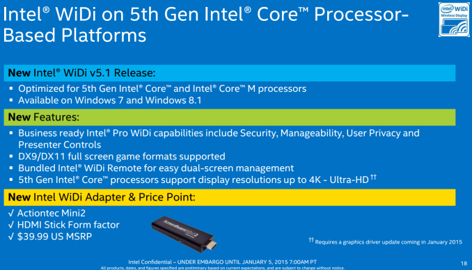
Also new on the table is WiDi 5.1, which brings support for 4K to the ecosystem.
A part of WiDi that has been lacking has been the business features, and as a result Intel is focusing on security, privacy and controls needed for a professional environment. These will need a driver update for the ultra-early adopters of Broadwell, but Intel is driving down the costs of the WiDi adapters to a more palatable price point. My Belkin WiDi receiver, for example, retailed at 120 GBP-ish back in 2013 and requires an external power supply. Compare that to the product Intel promoted with their conference call - the Actiontec Mini2 which uses HDMI and is only $40.
Intel Wireless AC-7265
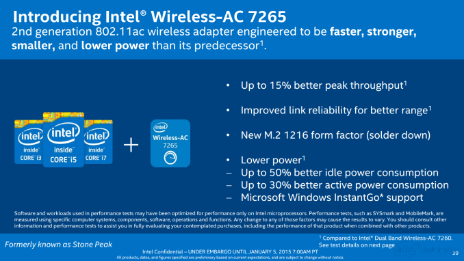
While not strictly speaking new to the market, Intel is promoting its new low power WiFi solution to the manufacturers to use in conjunction with Broadwell. The AC 7265 is an upgrade over the AC 7260 that was used extensively in Haswell from mobile devices all the way up to big desktop partners, and the AC 7265 brings about both performance and power benefits.
The form factor specifically for Broadwell-U is provided as a BGA M.2 part, with the package being 12mm x 16mm (given by the 1216 form factor designation). Low powered wireless is an important part of lower performance systems, as without the right configuration a sustained network load can eat up a portion of the processor performance. Intel’s partners with Broadwell-U are presumably not bound to use the AC 7265 and can use other products based on other performance metrics, but Intel is targeting networking as a source of power drain and working to correct that issue.
Devices! Where and When?
Most of AnandTech are here in Vegas, attending CES 2015 and (almost literally) running between meetings, press events and product showcases. Broadwell-U is high on our priority list, and we know several are due for announcement this week. Watch this space.

_thumb.png)
_thumb.png)

