Original Link: https://www.anandtech.com/show/8747/samsung-ssd-850-evo-review
Samsung SSD 850 EVO (120GB, 250GB, 500GB & 1TB) Review
by Kristian Vättö on December 8, 2014 10:00 AM EST
Samsung hasn't stopped impressing me in the SSD space. The early Samsung SSDs weren't very good, but ever since the introduction of the SSD 830 Samsung has been doing a brilliant job and has been setting the bar for performance, cost and reliability. The SSD 840 specifically showed what properly executed vertical integration can really do as Samsung was the first manufacturer to utilize TLC NAND in a client SSD. It took a whopping two years before the rest of the industry was able to follow Samsung's footsteps and even today SanDisk is still the only other vendor with a TLC SSD.
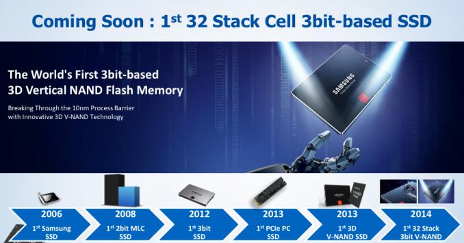
While getting an early lead on TLC NAND was a major win for Samsung and a showcase of its engineering talent, the real bombshell was dropped a year later at Flash Memory Summit 2013. For years it had been known that traditional NAND scaling would soon come to an end and that there is an alternate way of scaling in the horizon. As the first manufacturer in the world, Samsung announced that it had begun the mass production of its 128Gbit 24-layer 3D V-NAND.
It took another year before V-NAND found its way into a retail product, but it acquitted all of its promises when it finally did. The SSD 850 Pro is hands down the fastest SATA SSD on the market and it's also backed up by an industry-leading warranty and endurance rating – all which is thanks to V-NAND.
The SSD 850 Pro excels in performance and features, but given its high-end focus it's not a cost efficient solution for the majority of consumers. At this year's Flash Memory Summit, Samsung teased us about an upcoming TLC V-NAND SSD, which would solve the cost issue while still providing all the benefits of 3D NAND technology. The waiting is now over and the drive is (unsurprisingly) called the SSD 850 EVO.
In terms of capacities the 850 EVO lineup is similar to the 840 EVO. The only difference is that the 850 EVO drops the 750GB model, which from what I've heard wasn't a very popular model and to be honest it was kind of an odd middle capacity that generally wasn't price competitive against the 500GB and 1TB models. Initially I was told that the 850 EVO would come in 2TB capacity as well, but later on Samsung opted against it due to the limited demand. Samsung has always been after the high volume markets, so I see the logic behind the decision not to release a 2TB model just yet as its price would drive most people away. The good news, however, is that Samsung has the technology to bring a 2TB drive to the market.
| Samsung SSD 850 EVO Specifications | |||||
| Capacity | 120GB | 250GB | 500GB | 1TB | |
| Controller | Samsung MGX | Samsung MEX | |||
| NAND | Samsung 128Gbit 40nm TLC V-NAND | ||||
| DRAM (LPDDR2) | 256MB | 512MB | 1GB | ||
| Sequential Read | 540MB/s | 540MB/s | 540MB/s | 540MB/s | |
| Sequential Write | 520MB/s | 520MB/s | 520MB/s | 520MB/s | |
| 4KB Random Read | 94K IOPS | 97K IOPS | 98K IOPS | 98K IOPS | |
| 4KB Random Write | 88K IOPS | 88K IOPS | 90K IOPS | 90K IOPS | |
| DevSleep Power Consumption | 2mW | 2mW | 2mW | 4mW | |
| Slumber Power Consumption | 50mW | ||||
| Active Power Consumption (Read/Write) | Max 3.7W / 4.4W | ||||
| Encryption | AES-256, TCG Opal 2.0, IEEE-1667 (eDrive) | ||||
| Endurance | 75TB (41GB/day) | 150TB (82GB/day) | |||
| Warranty | Five years | ||||
The first hint of the capability of TLC V-NAND is the endurance ratings. The 120GB and 250GB capacities are rated at 75TB, which is fairly average, but the 500GB and 1TB models match up with the 850 Pro with their 150TB write endurance. I'll be talking a bit more about the NAND and testing its P/E cycle rating on the following pages, but it's clear that 3D NAND technology is taking TLC NAND to a whole new level in terms of endurance. Thanks to the more durable NAND, Samsung is also upping the warranty from three to five years, which is always a welcome upgrade and I think too many vendors have been fixated on three-year warranties even though NAND endurance has never been the limiting factor.
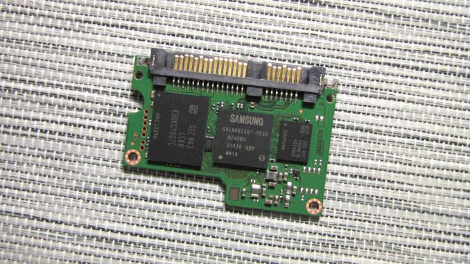
The new MGX controller in 120GB 850 EVO
In addition to the NAND, the 850 EVO sees an evolution in the controller. The 120GB, 250GB and 500GB models now come with a newer generation MGX controller, although unfortunately I have very few details as Samsung couldn't get me the information about the new controller ahead of the embargo lift. I've heard the MGX is a dual core design, whereas the MEX in the 1TB model (and 840 EVO & 850 Pro) features three ARM Cortex R4 cores. The reason behind the change is increased power efficiency and supposedly the third core isn't needed with the smaller capacities as there are less pages/blocks to track and thus NAND management requires less processing power. I'm guessing that the MGX is also manufactured with a smaller process node and the two cores run at a higher clock speed, but for now I don't have any concrete information backing that up.
The 850 EVO also features the common Samsung feature set. DevSleep, hardware-accelerated encryption (TCG Opal 2.0 & IEEE-1667) and RAPID are all supported. With the 850 Pro Samsung introduced RAPID 2.0 that upped the maximum RAM allocation to 4GB (with 16GB or more RAM installed in the system) and as one would expect the 850 EVO supports the updated version of RAPID. In fact, with the release of Magician 4.5 (included on the CD that is found in the retail package), RAPID sees an update to 2.1 version, although this is merely an incremental update with enhanced error handling and fixed compatibility issues with Intel's Rapid Storage Technology drivers.
Pricing
The always-so-important question is the price. All modern SSDs are relatively good (especially when compared against what we had three years ago), so for the majority of buyers the key factor is the price. Lately we have seen some very aggressive pricing from the likes of Crucial and SanDisk, and I was expecting that the 850 EVO would be Samsung's answer to that.
| Samsung SSD 850 EVO MSRPs | ||||
| Capacity | 120GB | 250GB | 500GB | 1TB |
| MSRP | $100 | $150 | $270 | $500 |
Unfortunately, the MSRPs at least are fairly high. I was told that the higher production costs of V-NAND necessitate the higher prices, which is why Samsung can't go directly against the MX100 and Ultra II, but in return Samsung offers a longer warranty, higher endurance and better performance (we will find out about the last one soon). That said, MSRPs have never been great indicators of final street prices and we may see the 850 EVO become more competitive eventually.
Test Systems
For AnandTech Storage Benches, performance consistency, random and sequential performance, performance vs transfer size and load power consumption we use the following system:
| CPU | Intel Core i5-2500K running at 3.3GHz (Turbo & EIST enabled) |
| Motherboard | ASRock Z68 Pro3 |
| Chipset | Intel Z68 |
| Chipset Drivers | Intel 9.1.1.1015 + Intel RST 10.2 |
| Memory | G.Skill RipjawsX DDR3-1600 4 x 8GB (9-9-9-24) |
| Video Card | Palit GeForce GTX 770 JetStream 2GB GDDR5 (1150MHz core clock; 3505MHz GDDR5 effective) |
| Video Drivers | NVIDIA GeForce 332.21 WHQL |
| Desktop Resolution | 1920 x 1080 |
| OS | Windows 7 x64 |
Thanks to G.Skill for the RipjawsX 32GB DDR3 DRAM kit
For slumber power testing we used a different system:
| CPU | Intel Core i7-4770K running at 3.3GHz (Turbo & EIST enabled, C-states disabled) |
| Motherboard | ASUS Z87 Deluxe (BIOS 1707) |
| Chipset | Intel Z87 |
| Chipset Drivers | Intel 9.4.0.1026 + Intel RST 12.9 |
| Memory | Corsair Vengeance DDR3-1866 2x8GB (9-10-9-27 2T) |
| Graphics | Intel HD Graphics 4600 |
| Graphics Drivers | 15.33.8.64.3345 |
| Desktop Resolution | 1920 x 1080 |
| OS | Windows 7 x64 |
- Thanks to Intel for the Core i7-4770K CPU
- Thanks to ASUS for the Z87 Deluxe motherboard
- Thanks to Corsair for the Vengeance 16GB DDR3-1866 DRAM kit, RM750 power supply, Hydro H60 CPU cooler and Carbide 330R case
Inside The Drives
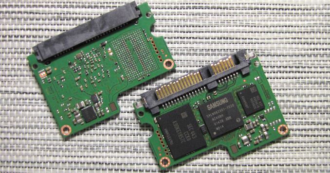
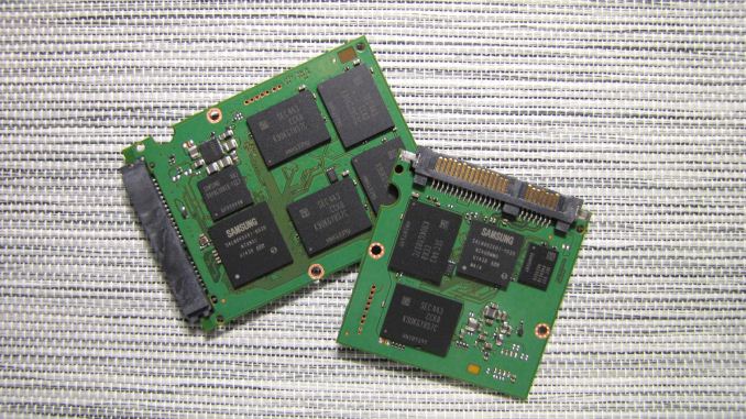
There are three different PCB designs in the 850 EVO lineup. The 120GB and 250GB models (above) use a tiny PCB with room for two NAND packages (one on each side). Interestingly enough, both use octal-die packages, meaning that the 120GB 850 EVO only has a single 128GB (8*16GB) NAND package. Decoding the part number reveals that the packages are equipped with eight chip enablers (CEs), so a single NAND package is viable since all eight dies can be accessed simultaneously.
The use of octal-die packages is actually true for all capacities. It's an interesting choice nevertheless, but I suspect Samsung's packaging technology is advanced and mature enough that it's more cost efficient to use high die count packages and small PCBs instead of larger PCBs with more and less dense NAND packages.
| Samsung SSD 850 EVO NAND Configurations | ||||
| Capacity | 120GB | 250GB | 500GB | 1TB |
| # of NAND Packages | 1 | 2 | 4 | 8 |
| # of Die Per Package | 8 | 8 | 8 | 8 |
| Total # of Die | 8 | 16 | 32 | 64 |
| Die Capacity | 128Gbit | 128Gbit | 128Gbit | 128Gbit |
| Raw NAND Capacity | 128GiB | 256GiB | 512GiB | 1024GiB |
| Over-Provisioning | 12.7% | 9.1% | 9.1% | 9.1% |
TurboWrite
TurboWrite is a feature that Samsung brought to the 840 EVO to increase write performance. The idea of running a small portion of the NAND in SLC mode was nothing new, but it was the first time it truly made sense because the 840 EVO used slower TLC NAND and hence the SLC buffer could provide significant improvements to write performance and user experience. Unsurprisingly, TurboWrite is also present in the 850 EVO.
| Samsung SSD 850 EVO TurboWrite SLC Buffer Size | ||||
| Capacity | 120GB | 250GB | 500GB | 1TB |
| TurboWrite Buffer Size | 3GB | 3GB | 6GB | 12GB |
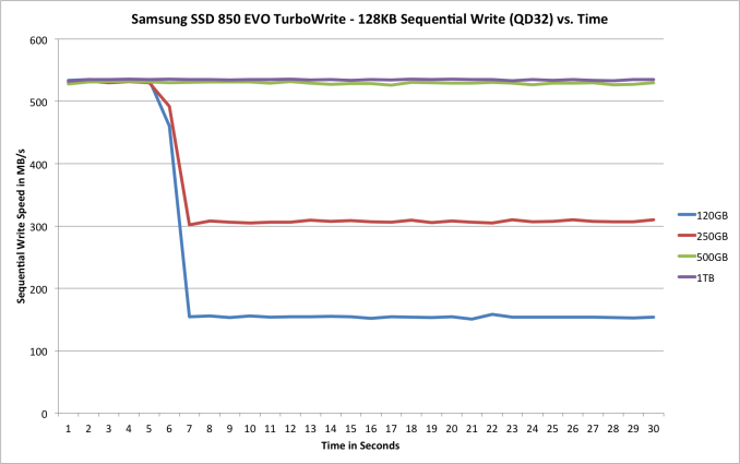
The buffer sizes and core architecture have remained unchanged. All writes hit the SLC buffer first, from which they then get moved to the TLC array during idle time. The only exception is a case of long, sustained period of writes that exceeds the buffer size, in which case the data will be written straight to the TLC portion.
| Write Performance With and Without TurboWrite | ||||
| With TurboWrite | Without TurboWrite | |||
| Sequential Write | 4KB Random Write (QD32) | Sequential Write | 4KB Random Write (QD32) | |
| 120GB | 520MB/s | 88K IOPS | 150MB/s | 38K IOPS |
| 250GB | 520MB/s | 88K IOPS | 300MB/s | 70K IOPS |
| 500GB | 520MB/s | 90K IOPS | 500MB/s | 80K IOPS |
| 1TB | 520MB/s | 90K IOPS | 520MB/s | 80K IOPS |
Samsung's reviewer's guide states that the 850 EVO features "enhanced TurboWrite technology" with a focus on random write performance, but I don't have any additional details as to how the TurboWrite implementation in the 850 EVO differs from the 840 EVO. TurboWrite was always designed to cache all writes regardless of the nature of the write (random vs sequential), so I'm not sure if anything has actually changed. Obviously the algorithms have been optimized for the new NAND and controller architecture and it's possible that the whole batch of algorithms has improved in the process, but I'll provide an update when I hear back from Samsung.
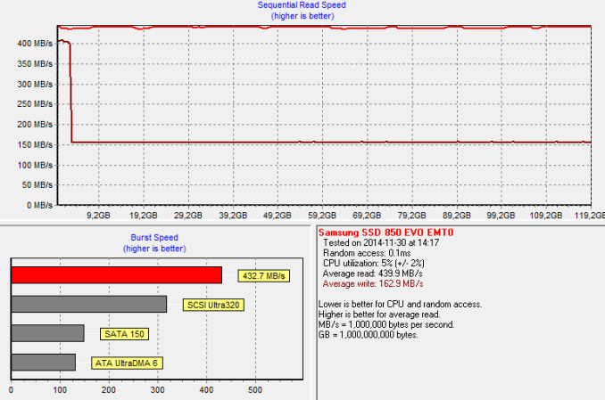
I ran a quick sequential write test to see how TurboWrite behaves in the 850 EVO. At smaller capacities it clearly provides a tremendous performance boost, but at 500GB and 1TB there is enough NAND to provide the parallelism that is needed to max out the SATA 6Gbps interface. That is a big improvement over the 840 EVO as its write performance maxed out at ~400MB/s when writing to the TLC array, so the performance benefits of 3D NAND technology are already evident.
Three Bits and Three Dimensions: What's the Deal?
I've covered 3D NAND and TLC NAND in detail in the past and in this article I'll just explain what 3D technology means to TLC NAND and vice versa, so head over to the links above if you are in the search for a deeper analysis of the two technologies.
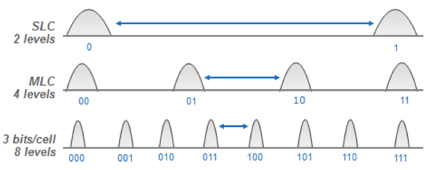
Truth to be told, 3D technology is ideal for TLC. The fundamental problem of TLC NAND has always been the limited endurance and performance, which is caused by the additional voltage states that are needed to store three bits (i.e. eight possible bit outputs) in one cell. With eight voltage states compared to four in MLC, TLC NAND is less resistant to wear out because it takes a smaller change in the cell charge to corrupt the cell value. Due to the way NAND works, the cells (or the insulators in the cell to be exact) wear out over time, which induces electron leakage that alters the cell charge and hence the voltage state. This gets worse with die shrinks because the number of electrons decreases, making the NAND even less tolerant to wear out.
The key aspect of 3D V-NAND is the process node. By going back to 40nm lithography, the number of electrons increase exponentially, which makes TLC a much more viable technology than it was with modern planar NAND. Obviously, V-NAND doesn't change the basics of TLC NAND because it still takes eight voltage states to differentiate all the possible 3-bit outputs, but thanks to the increased number of electrons there is more breathing room between the states and thus the cells are more error tolerant.
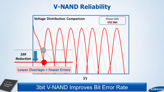
Samsung claims 10x reduction in voltage state overlaps, which is a massive change for the better. You can see how crammed the planar TLC voltage states are, so it's no wonder that the endurance is low because the states are practically overlapping at each point in the voltage distribution and hence even tiny changes in the cell voltage can alter the cell's voltage state.
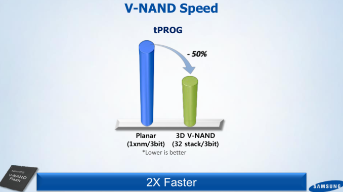
The larger cell structure also enables higher performance because it takes less iterations to program a cell. With planar TLC NAND it took multiple very high voltage pulses as well as numerous verification process to reach the right charge, but with looser voltage distribution the programming process has less steps and thus takes less time.
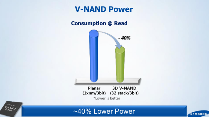
And given the lower read/program latencies and less need for error correction, the power consumption is also considerably lower.
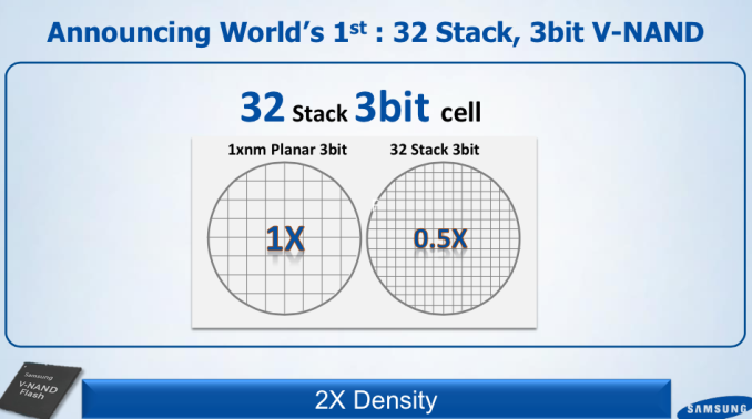
In addition to better latency and power consumption characteristics, Samsung claims doubled the density over its 19nm planar TLC NAND, but without knowing the die size of 128Gbit 32-layer TLC V-NAND, it's hard to say how accurate this is. There have been some whispering that the 128Gbit die would actually be identical to the 86Gbit MLC die because 86Gbit multiplied by 1.5 equals 129Gbit and at the silicon level MLC and TLC aren't any different, but for now that's just speculation.
What I do know is that Samsung started the mass production of TLC V-NAND later, which suggests that the two aren't completely uniform. Moreover, from what I know TLC NAND requires some changes to the peripheral circuitry in order to read three bits from one cell, so while the NAND memory arrays could be alike the die size is still likely at least slightly different. Anyway, we'll find out when Chipworks (or some other silicon analysis company) takes a closer look at the NAND die itself.
Endurance: Close to Planar MLC NAND
The big question with every new NAND generation is the endurance. We already saw 6,000 P/E cycles in the SSD 850 Pro and an amazing 40,000 P/E cycles in the SSD 845DC Pro, which proved that V-NAND provides substantially better endurance over today's planar NAND nodes. However, endurance was never really an issue with planar MLC NAND except in the enterprise space, so the 850 EVO with its TLC V-NAND offers a much more interesting insight to the capability of 3D NAND technology.
To test endurance, I put the 120GB 850 EVO through our usual endurance test suite. Basically I just used Iometer to write 128KB sequential data at queue depth of 1 to the drive while monitoring the Wear Leveling Count (WLC) and Total LBAs Written SMART values. The 'Current Value' of the WLC SMART value gives the remaining endurance as a percentage (starts from 99), whereas the 'Raw Data' value indicates the number of consumed P/E cycles. In order to estimate the endurance, I had to find the spot where the increase in 'Raw Data' value decreases the 'Current Value' by one.
| Samsung SSD 850 EVO Endurance | |
| Change in Current Wear Leveling Count Value | 6 |
| Change in Raw Wear Leveling Count Value | 128 |
| Total Data Written | 15,260GiB |
| Estimated Total Write Endurance | 254,325GiB |
| Observed Number of P/E Cycles | 1,987 |
It appears that TLC flavor of V-NAND is rated at about 2,000 P/E cycles. The raw WLC value seems to be based on the user capacity (i.e. 120GB = 1 P/E cycle) because just going by it puts the endurance at ~2,133 P/E cycles (128/0.06), but that doesn't add up with the raw NAND capacity and total data written. However, the estimated total write endurance (which is just 15,260/0.06) suggests that the NAND itself is rated at 2,000 P/E cycles, which would make sense as the number of P/E cycles is usually an even thousand and it's also inline with the increase that the 850 Pro saw (from 3,000 cycles in the 840 Pro to 6,000 cycles).
| Samsung SSD 850 EVO Lifetime Estimation | ||||
| 120GB | 250GB | 500GB | 1TB | |
| Raw NAND Capacity | 128GiB | 256GiB | 512GiB | 1024GiB |
| NAND P/E Cycles | 2,000 | |||
| Raw NAND Endurance | 250TiB | 500TiB | 1000TiB | 2000TiB |
| Lifespan with 20GiB of Host Writes per Day with 1.5x Write Amplification | 23.4 years | 46.8 years | 93.5 years | 187.0 years |
| Lifespan with 100GiB of Host Writes per Day with 3x Write Amplification | 2.3 years | 4.7 years | 9.4 years | 18.7 years |
While write endurance in client workloads was never truly an issue even with planar TLC NAND, the doubled endurance in TLC V-NAND makes it practically impossible to wear out the drive before it has become totally obsolete. Only some very extreme workloads could wear out the smaller capacities before the warranty runs out, but the 850 EVO is a wrong drive for such workloads in the first place. All in all, there should be absolutely no reason to worry about the endurance of the 850 EVO, especially given the endurance ratings Samsung is giving to the 850 EVO (75TB for 120/250GB and 150TB for 500GB/1TB).
Performance Consistency
Performance consistency tells us a lot about the architecture of these SSDs and how they handle internal fragmentation. The reason we do not have consistent IO latency with SSDs is because inevitably all controllers have to do some amount of defragmentation or garbage collection in order to continue operating at high speeds. When and how an SSD decides to run its defrag or cleanup routines directly impacts the user experience as inconsistent performance results in application slowdowns.
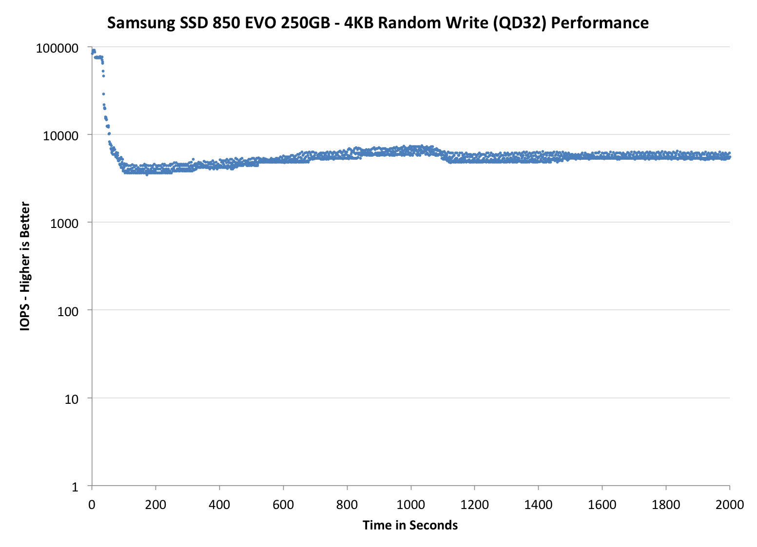
To test IO consistency, we fill a secure erased SSD with sequential data to ensure that all user accessible LBAs (Logical Block Addresses) have data associated with them. Next we kick off a 4KB random write workload across all LBAs at a queue depth of 32 using incompressible data. The test is run for just over half an hour and we record instantaneous IOPS every second.
We are also testing drives with added over-provisioning by limiting the LBA range. This gives us a look into the drive’s behavior with varying levels of empty space, which is frankly a more realistic approach for client workloads.
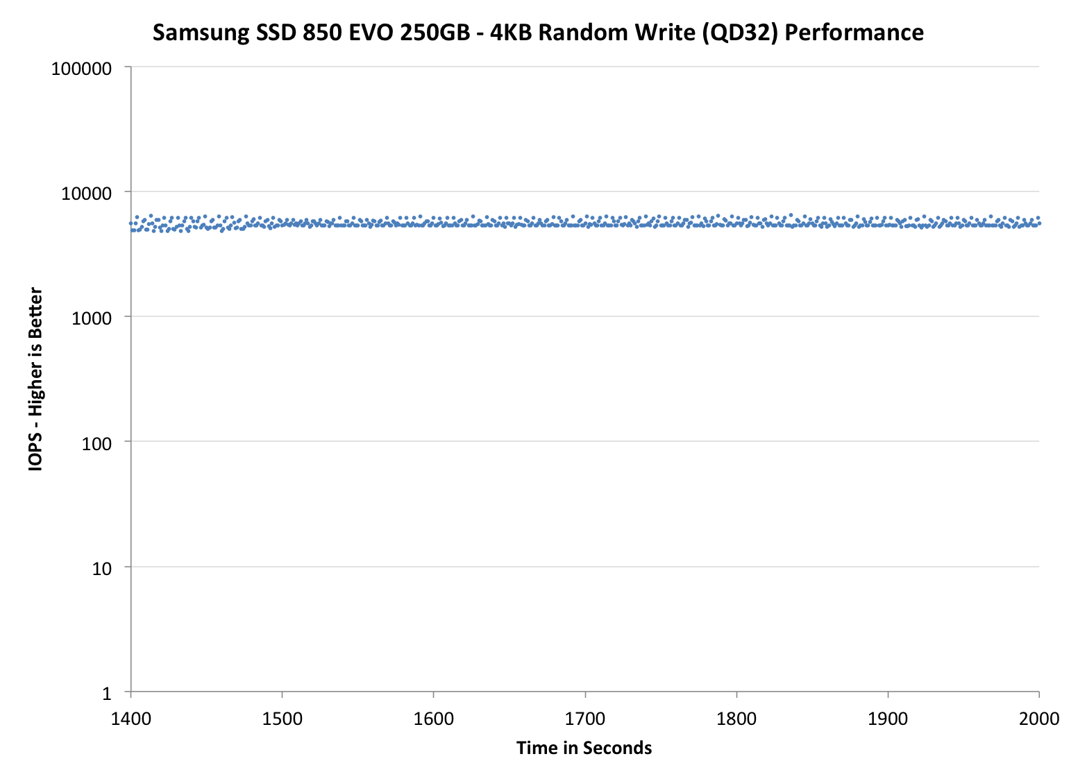
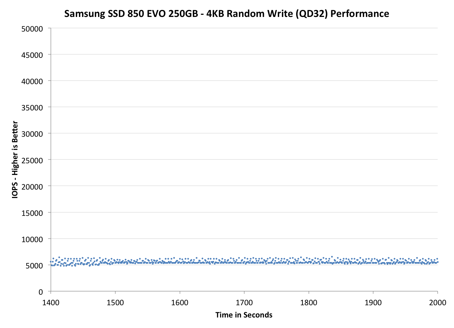
Each of the three graphs has its own purpose. The first one is of the whole duration of the test in log scale. The second and third one zoom into the beginning of steady-state operation (t=1400s) but on different scales: the second one uses log scale for easy comparison whereas the third one uses linear scale for better visualization of differences between drives. Click the dropdown selections below each graph to switch the source data.
For more detailed description of the test and why performance consistency matters, read our original Intel SSD DC S3700 article.
 |
|||||||||
| Default | |||||||||
| 25% Over-Provisioning | |||||||||
The 850 EVO presents a healthy increase in IO consistency. The 840 EVO wasn't exactly inconsistent in the first place, but the 850 EVO takes the steady-state IOPS from ~3,000-5,000 IOPS to 5,000-8,000 IOPS, which is actually nearly on par with the 850 Pro. The 850 EVO has without a doubt one of the highest performance consistencies out of the value/mainstream drives we have tested.
 |
|||||||||
| Default | |||||||||
| 25% Over-Provisioning | |||||||||
 |
|||||||||
| Default | |||||||||
| 25% Over-Provisioning | |||||||||
TRIM Validation
To test TRIM, I filled a 120GB 850 EVO with sequential 128KB data and proceeded with a 30-minute random 4KB write (QD32) workload to put the drive into steady-state. After that I TRIM'ed the drive by issuing a quick format in Windows and ran HD Tach to produce the graph below.
And TRIM works as expected.
AnandTech Storage Bench 2013
Our Storage Bench 2013 focuses on worst-case multitasking and IO consistency. Similar to our earlier Storage Benches, the test is still application trace based – we record all IO requests made to a test system and play them back on the drive we are testing and run statistical analysis on the drive's responses. There are 49.8 million IO operations in total with 1583.0GB of reads and 875.6GB of writes. I'm not including the full description of the test for better readability, so make sure to read our Storage Bench 2013 introduction for the full details.
| AnandTech Storage Bench 2013 - The Destroyer | ||
| Workload | Description | Applications Used |
| Photo Sync/Editing | Import images, edit, export | Adobe Photoshop CS6, Adobe Lightroom 4, Dropbox |
| Gaming | Download/install games, play games | Steam, Deus Ex, Skyrim, Starcraft 2, BioShock Infinite |
| Virtualization | Run/manage VM, use general apps inside VM | VirtualBox |
| General Productivity | Browse the web, manage local email, copy files, encrypt/decrypt files, backup system, download content, virus/malware scan | Chrome, IE10, Outlook, Windows 8, AxCrypt, uTorrent, AdAware |
| Video Playback | Copy and watch movies | Windows 8 |
| Application Development | Compile projects, check out code, download code samples | Visual Studio 2012 |
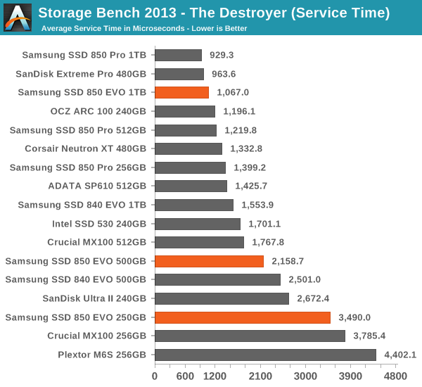
We are reporting two primary metrics with the Destroyer: average data rate in MB/s and average service time in microseconds. The former gives you an idea of the throughput of the drive during the time that it was running the test workload. This can be a very good indication of overall performance. What average data rate doesn't do a good job of is taking into account response time of very bursty (read: high queue depth) IO. By reporting average service time we heavily weigh latency for queued IOs. You'll note that this is a metric we have been reporting in our enterprise benchmarks for a while now. With the client tests maturing, the time was right for a little convergence.
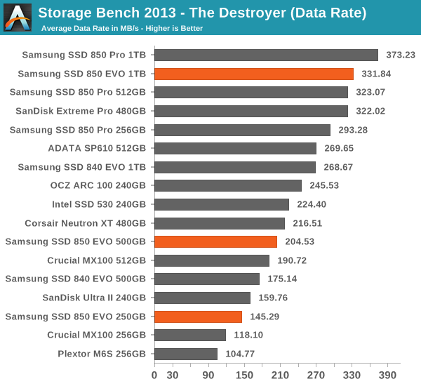
The faster NAND and better IO consistency results in increased performance in our 2013 Storage Bench. The 1TB version shines in the test and isn't far from the 850 Pro, but the 500GB and 250GB models end up being middle-class performers. Especially the performance of the 250GB model is a bit underwhelming because it is beaten by the Ultra II, even though the 850 EVO should have a performance advantage thanks to V-NAND.
AnandTech Storage Bench 2011
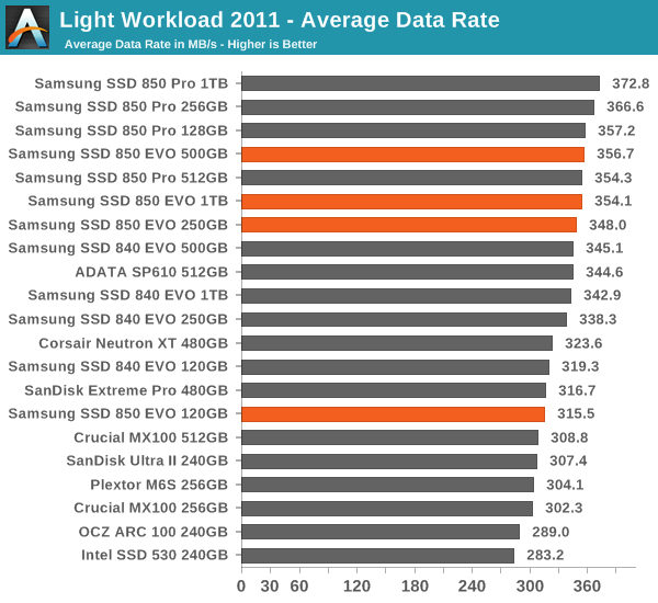
Back in 2011 (which seems like so long ago now!), we introduced our AnandTech Storage Bench, a suite of benchmarks that took traces of real OS/application usage and played them back in a repeatable manner. The MOASB, officially called AnandTech Storage Bench 2011 – Heavy Workload, mainly focuses on peak IO performance and basic garbage collection routines. There is a lot of downloading and application installing that happens during the course of this test. Our thinking was that it's during application installs, file copies, downloading and multitasking with all of this that you can really notice performance differences between drives. The full description of the Heavy test can be found here, while the Light workload details are here.
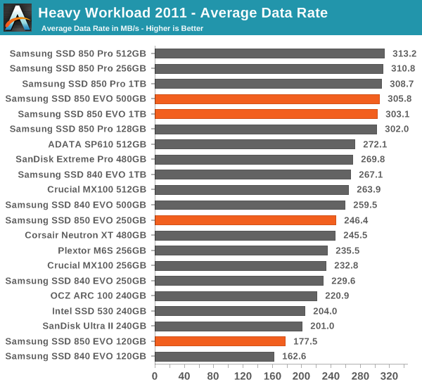
Fortunately the 850 EVO does much better in our 2011 Storage Benches, which are more representative of what a typical consumer would subject the drive to. In these tests the 850 EVO is actually more or less a match for the 850 Pro (excluding the 120GB model) and beats pretty much all of its main competitors (namely MX100 and Ultra II).
Random Read/Write Speed
The four corners of SSD performance are as follows: random read, random write, sequential read and sequential write speed. Random accesses are generally small in size, while sequential accesses tend to be larger and thus we have the four Iometer tests we use in all of our reviews.
Our first test writes 4KB in a completely random pattern over an 8GB space of the drive to simulate the sort of random access that you'd see on an OS drive (even this is more stressful than a normal desktop user would see). We perform three concurrent IOs and run the test for 3 minutes. The results reported are in average MB/s over the entire time.
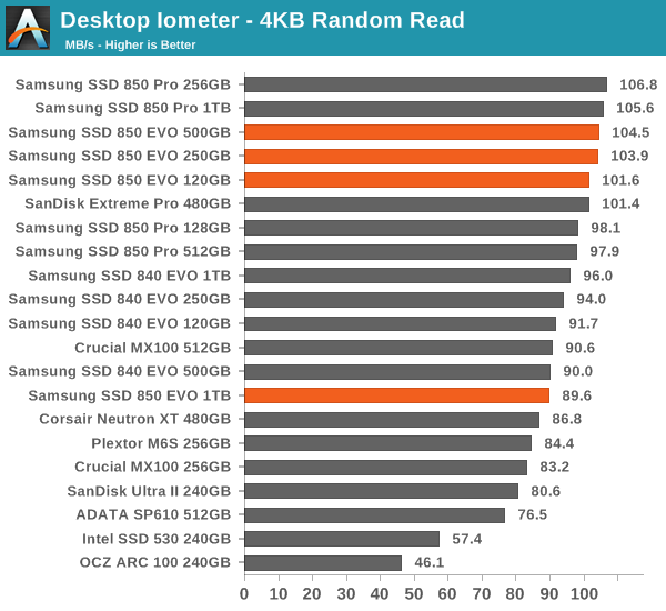
The models with the new MGX controller enjoy excellent random read performance, although the 1TB version isn't bad either. Without knowing the specifications of the MGX controller, it's hard to know what is causing the performance increase, but I still suspect it is due to a higher clock speed.
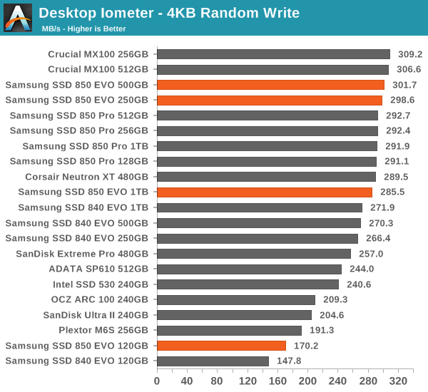
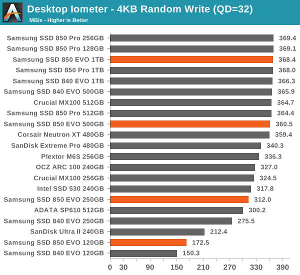
Random write performance also sees an increase across all capacities and is more or less on par with the 850 Pro at larger capacities.
Sequential Read/Write Speed
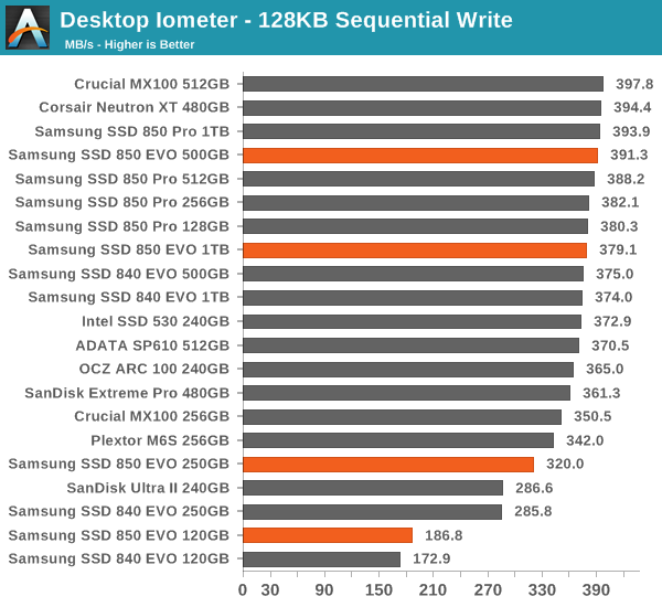
To measure sequential performance we run a 1 minute long 128KB sequential test over the entire span of the drive at a queue depth of 1. The results reported are in average MB/s over the entire test length.
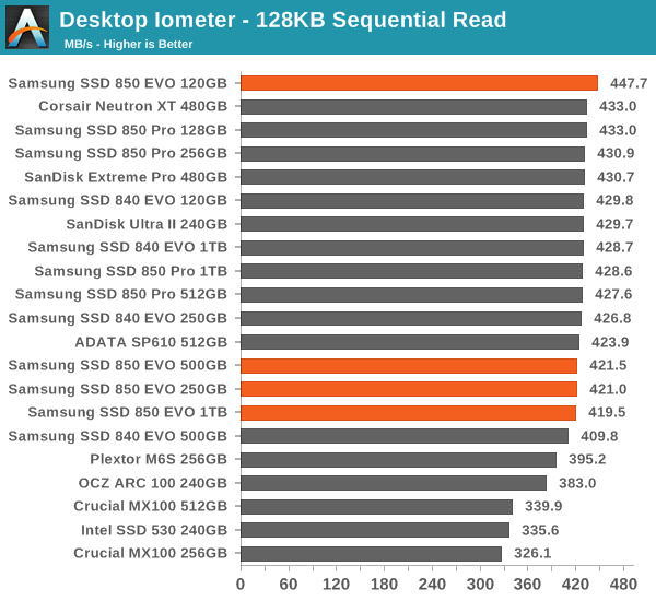
Sequential performance doesn't present any real surprises. Write speed at smaller capacities gets a small boost, but other than that the performance is typical SATA 6Gbps level.
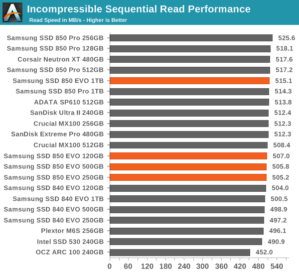
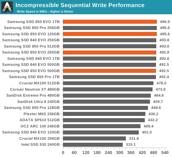
AS-SSD Incompressible Sequential Read/Write Performance
The AS-SSD sequential benchmark uses incompressible data for all of its transfers. The result is a pretty big reduction in sequential write speed on SandForce based controllers, but most other controllers are unaffected.
Performance vs. Transfer Size
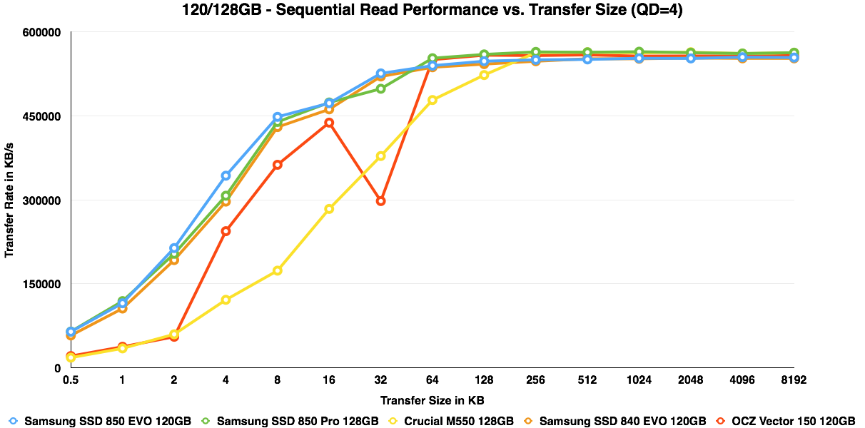
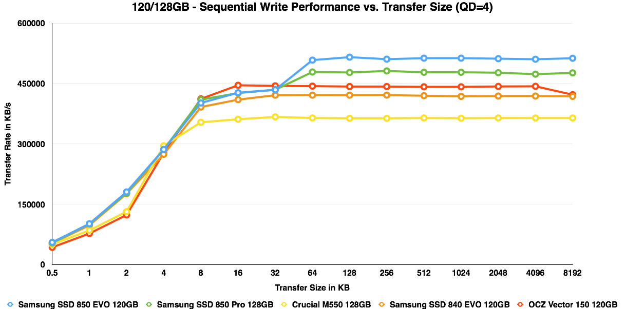
ATTO is a useful tool for quickly benchmarking performance across various transfer sizes. You can get the complete data set in Bench. The performance of the 850 EVO scales excellently across all transfer sizes, although I should note that TurboWrite has its fingers in play as ATTO's test size maxes out at 2GB, which is small enough that it will get written to the SLC buffer.
Power Consumption
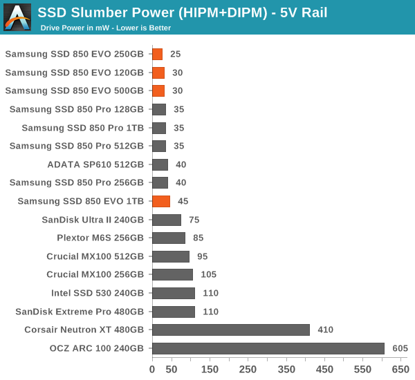
Samsung has always done a great job at power efficiency and the 850 EVO is no exception. In slumber mode the 850 EVO is one of the most efficient drives we have seen and it also explains why Samsung went with the new MGX controller as the 500GB and smaller capacities consume about 30% less power than the 1TB model.
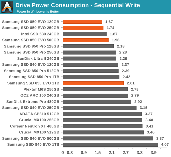
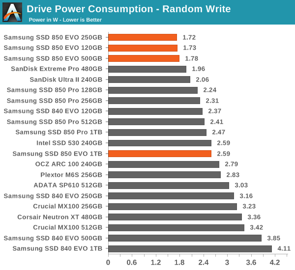
Load power consumption is also exceptional, although once again I should note that the writes are hitting the SLC buffer, which is more power efficient than writing to the TLC array. Right after I stopped writing to the drive I saw the power consumption increase to ~3W while the drive was reading data from SLC and writing it to TLC, but that didn't take longer than 10-20 seconds or so (though it depends on how much you write to the drive). I have some tests prepared for our 2015 SSD suite that will look at power over time more closely, so it will also better account for SLC to MLC/TLC writes.
Final Words
The 850 EVO is yet another showcase of Samsung's engineering talent and truth to be told there is a lot of good in the 850 EVO. By combining TLC with V-NAND technology, Samsung is eliminating any and all concerns that people might have had about the endurance of TLC NAND and to back that up Samsung is rating the 850 EVO's endurance higher than the MLC drives of most manufacturers. I never considered the endurance of TLC NAND to be an issue for average client workloads, but I saw many people who were doubtful about the sufficiency of 1,000 P/E cycles, so with twice that in TLC V-NAND I believe many will and should stop treating TLC as a second class citizen.
Not only is the endurance higher, but the 850 EVO's performance is also better compared to its predecessor. In our 2011 Storage Benches the 850 EVO matches up with the 850 Pro and is hence one of the fastest SATA 6Gbps SSDs for typical client workloads. In very heavy workloads, illustrated by our 2013 Storage Bench, the 850 EVO does okay, but it's clear that it's outperformed by drives that are more optimized for such usage.
| NewEgg Price Comparison (12/7/2014) | ||||
| 120/128GB | 240/250/256GB | 480/500/512GB | 960GB/1TB | |
| Samsung SSD 850 EVO (MSRP) | $100 | $150 | $270 | $500 |
| Samsung SSD 850 Pro | $105 | $180 | $320 | $630 |
| Samsung SSD 840 EVO | $85 | $125 | $230 | $440 |
| SanDisk Extreme Pro | - | $150 | $328 | $531 |
| SanDisk Ultra II | $80 | $110 | $220 | $420 |
| Crucial MX100 | $70 | $113 | $215 | - |
| Crucial M550 | $85 | $163 | $265 | $450 |
| Plextor M6S | $80 | $158 | $290 | - |
| Intel SSD 730 | - | $130 | $220 | - |
| Intel SSD 530 | $75 | $130 | $240 | - |
| OCZ ARC 100 | $70 | $100 | $215 | - |
There is one huge 'but' however – the price. The 850 EVO is a very competitive drive in performance and features, but neither of these warrants the premium Samsung is charging. As I've said before, there are only two main segments in the SSD market that I recognize, which are the value/mainstream and high-end/enthusiast segments.
For the value segment, the key consideration is the price because these are typically users who don't push their systems to the limits and thus shouldn't pay a premium for a performance increase that is likely to be negligible for their usage. Our Light Workload suite highlights this pretty well because the difference between most drives is on the order of 10-20% and while a possible 10% increase in performance would be worth $5, $10 and maybe even $20 to some users, it's definitely not worth the ~$50 Samsung is charging for the 850 EVO over Crucial's MX100 and SanDisk's Ultra II for example.
As for the high-end segment, Samsung already has that one covered by the 850 Pro. The 850 EVO, especially at the smaller capacities, isn't fast enough under IO intensive workloads to really compete with the 850 Pro and Extreme Pro. Given that the Extreme Pro can be had for about the same cost (depending on the capacity, of course), I would much rather have that if I was looking for a high-end SSD.
In other words, the 850 EVO falls into the infamous middle-class. It doesn't have an obvious niche in the market because it's too expensive for the value-oriented buyer and it's not fast enough to be considered as a competitive high-end SSD. If Samsung shaved $30 to $50 off the price, the 850 EVO would be competitive against the other value drives because the five-year warranty and Samsung's top-of-the-class software suite add some value, but with the current pricing there are just better options on the market.
A part of me sees that it might have been worthwhile for Samsung to do one more planar NAND shrink to be more competitive in the mainstream segment because right now the 850 EVO is missing that market. While 3D NAND will eventually become more cost efficient as the number of layers increases, we are not there yet. I absolutely love all the performance and endurance benefits V-NAND is bringing to the table, but if the 850 EVO can't even compete with MLC drives in price, that's a bit alarming.
There is still hope that the MSRPs are just conservative and street prices could end up lower. If they don't, while the 850 EVO is clearly the best performing "value" drive, it likely won't see the same sort of success as its predecessor. Samsung also has a strong presence in the OEM desktop and laptop markets, but OEMs may not see enough to sway them over from the 840 EVO if prices are quite a bit higher.

