Original Link: https://www.anandtech.com/show/8718/the-samsung-galaxy-note-4-exynos-review
ARM A53/A57/T760 investigated - Samsung Galaxy Note 4 Exynos Review
by Andrei Frumusanu & Ryan Smith on February 10, 2015 7:30 AM EST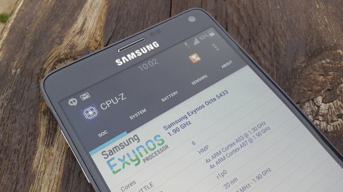
It's been over three months since Josh had the opportunity to review the Note 4 in its details. The defining characteristic of that review is that it was a look at the variant with Qualcomm's Snapdragon 805 SoC running at the heart of the device. This version is found in devices shipping in North America, Western Europe, China and Japan. While these markets have now been served by Qualcomm's silicon offerings, Samsung is now back on track at trying to expand its market-share of in-house Exynos SoCs. As such, all other markets (with small exceptions) seem to be getting served Exynos variants of the Note 4. While we normally try to cover all aspects of device performance, for this review we will focus on the SoC and the differences that result from this change.
Before we continue on, we'd like to thank international phone specialist 28Mobile.com for providing us with an Exynos unit of the Galaxy Note 4.
Model Breakdown
| Samsung Galaxy Note 4 Models | ||
| Samsung Galaxy Note 4 SM-N910 (F/A/V/T/P/06W/8V/G/0Z) |
Samsung Galaxy Note 4 SM-N910 (C/S/L/K/U/H) |
|
| SoC | 2.7 GHz Snapdragon 805 | 1.9GHz Exynos 5433 |
| RAM | 3GB 128-bit LPDDR3-1600 25.6GB/s bandwidth |
3GB 64-bit LPDDR3-1650 13.2GB/s bandwidth |
| NAND | Samsung 32/64GB NAND + microSD |
Samsung 32/64GB NAND + microSD |
| Display | 5.7” 1440p Super AMOLED | 5.7” 1440p Super AMOLED |
| Network | 2G / 3G / 4G LTE Qualcomm MDM9x35 Cat6 LTE (F) Qualcomm MDM9x25 Cat4 LTE (*) |
2G / 3G / 4G LTE Intel XMM7260 Cat.6 LTE (U) Samsung M303 Cat.6 LTE (S/K/L) Ericsson M7450 Cat.4 LTE (C) 2G / 3G Ericsson M7450 (H) |
| Dimensions | 153.5 x 78.6 x 8.5 mm, 176g | 153.5 x 78.6 x 8.5 mm, 176g |
| Camera | 16MP Rear Facing w/ OIS, 1/2.6" CMOS size, F/2.0 aperture (Sony IMX240) 3.7MP FFC w/ F/1.9 aperture (S.LSI S5K6D1) |
16MP Rear Facing w/ OIS, 1/2.6" CMOS size, F/2.0 aperture (Sony IMX240) 3.7MP FFC w/ F/1.9 aperture (S.LSI S5K6D1) |
| Battery | 3220 mAh, 3.85V, 12.397 Whr | 3220 mAh, 3.85V, 12.397 Whr |
| OS | Android 4.4.4 with TouchWiz UX | Android 4.4.4 with TouchWiz UX |
| Connectivity | 802.11a/b/g/n/ac + BT 4.1, USB2.0, GPS/GNSS, MHL, DLNA, NFC |
802.11a/b/g/n/ac + BT 4.1, USB2.0, GPS/GNSS, MHL, DLNA, NFC |
| SIM Size | MicroSIM | MicroSIM |
The model breakdown of the Note 4 is quite a mess. The S805 version breaks down into about 9 different local versions, each with different RF frequency support and varying modem configurations. The Exynos variants are even more convoluted in terms of modem choice. We've been reporting that we might see Intel's XMM7260 as the predominant modem in Samsung's SoCs, but that seems to have changed and the Intel modem is only shipped in a small percentage of total units on the SM-N910U model, which ships in South-East Asia.
In their home country of Korea Samsung continues to rely on their own modem, recently marketed as the "Exynos Modem" series. Samsung has been steadily developing their own modem hardware over the years and it seems the M303 is at feature parity with the Intel XMM7260 and Qualcomm's MDM9x35. This year Samsung has been pushing their modems outside of Korea in several devices such as the Galaxy S5 Mini, so I expect them in the future to be more prevalent in other global markets.
The surprise supplier and big winner of this generation is Ericsson; the M7450 is found in unarguably the largest portion of Exynos variants, the SM-910C and SM-910H, shipping throughout South America, Central and Eastern Europe, Africa, the Middle East, and some Asian countries. Brian first reported on this modem over 1.5 years ago and we haven't heard much about it since. The surprise here is that Ericsson managed to get such a big design win before announcing that they will discontinue development on modems altogether. The even more intriguing story is that the M7450 is used in the 3G version of the Note 4, usually a traditional Intel design win.
Whatever model you end up with, and as long as the frequency bands match your provider, the choice between Snapdragon and Exynos remains the biggest differentiation. Everything else from camera to WiFi to battery size remains the same in an identical form-factor.
For this review we're investigating the SM-910C running on firmware KTU84P.N910CXXU1ANJ8.
Exynos 5433 - The First Mobile ARM A57 SoC
I had reported back in September that Samsung's new Exynos 5433 found in the Note 4 is actually the first implementation of ARM's A53/A57 and T760 new SoC IP. While it took Samsung some time to actually officially announce the part, they eventually did confirm it. The interesting disclosure here is that they choose to market it in the Exynos 7 family, which certainly makes more sense than keeping it in the Exynos 5 category of SoCs.
Also in my initial article I shared my opinion that I doubted that Samsung would update the Note 4 to AArch64 - this was based on the fact that the kernel treats the SoC as an A7/A15 part and most of the software stack remained 32-bit. Events since then seem to point out that they will eventually upgrade it to 64-bit, since we're seeing official patches in upstream Linux with the chip being introduced with a full ARMv8 device tree. This is interesting to see and might point out that Samsung will go the effort to upgrade the BSPs to AArch64; however it remains unclear whether we'll see this on the Note 4. My personal opinion remains that we won't be seeing this overhaul in Samsung's 5.0 Lollipop update.
Let's take a look again at how things have evolved in terms of spec sheet since then:
| Samsung Exynos 5 Octa 2014 lineup | |||
| SoC | Samsung Exynos 5422 |
Samsung Exynos 5430 |
Samsung Exynos 5433 |
| CPU | 4x Cortex A7 r0p5 @1.3GHz 512KB L2 cache 4x Cortex A15 r2p4 @1.9GHz 2MB L2 cache |
4x Cortex A7 r0p5 @1.3GHz 512KB L2 cache 4x Cortex A15 r3p3 @1.8GHz 2MB L2 cache |
4x Cortex A53 [email protected] 256KB* L2 cache 4x Cortex A57 r1p0 @1.9GHz 2MB L2 cache |
| Memory Controller |
2x 32-bit @ 933MHz LPDDR3 14.9GB/s b/w |
2x 32-bit @ 825MHz LPDDR3 13.2GB/s b/w |
2x 32-bit @ 825MHz LPDDR3 13.2GB/s b/w |
| GPU | Mali T628MP6 @ 533MHz |
Mali T628MP6 @ 600MHz |
Mali T760MP6 @ 700MHz |
| Mfc. Process |
Samsung 28nm HKMG |
Samsung 20nm HKMG |
Samsung 20nm HKMG |
I've been able to confirm that the GPU on the 5433 is an MP6 configuration, meaning it sports the same amount of cores as the previous Mali T628 implementations in the 5430, 5422 and 5420. I've also acquired a Galaxy Alpha which I'll review at a later date, but noticed that Samsung is also shipping 825MHz memory on that device. As such, the bandwidth of the 5430 is corrected from the publicized 17GB/s down to 13.2GB/s.
Samsung has retained the cache sizes found in the older 54xx SoCs, meaning 512KB on the little cluster* We see a reduction to 256K on the L2 of the A53 cluster, and a continuation of 2MB on the big cluster. I would have liked to see the A53's getting 1MB of L2 but it seems we'll have to wait for future SoCs to see an improvement there.
In other regards, the 5433 differs very little from the 5430. It has almost identical auxiliary block IP, sharing the same ISP, hardware decoders and encoders, various interfaces, and a similar bus architecture.
* Correction 24/03/2015: Our initial info of 512K L2 cache on the A53 cluster was wrong and has henceforth been corrected to 256K (Source)
Miscellaneous differences
With the modem and SoC platform being the two main differences between the two Samsung devices, there are some other minor changes of components. On the audio side Qualcomm's WCD9330 is replaced by WolfsonMicro's WM5110 audio SoC. The Wolfson IC uses its integrated DSPs for voice processing, replacing the need for an additional Audience eS705 audio processing chip that is used in the Snapdragon variant. This might result in different call and audio quality between the two versions. The WM5110 also takes over device voice activation duties for the Exynos Note 4, which you can use with SVoice or Google Now.
I also noticed that yet again Samsung did not allow for native 44.1KHz audio playback in the default configuration of Android's AudioFlinger on the Exynos version, causing forced resampling of 44.1KHz content to 48KHz. Neither version allows for higher quality output, even though both audio solutions support 24-bit 192KHz audio in hardware. I'm not sure what Samsung's audio team is doing here but it's getting increasingly frustrating to see this issue continue, starting with the Galaxy S4.
In terms of media playback, Samsung has not exposed the HEVC/H265 hardware decoder of the Exynos 543X's to the media codec capabilities list of the system. The device is still shipping with the decoder block's firmware, so again this is either an oversight or something has gone wrong during development of the device. The Qualcomm version exposes the HEVC decoder of the Snapdragon 805.
A large functional difference between recent Exynos SoCs and Qualcomm variants comes with the capability of the display controller. Due to 1440*2560*32bpp*60fps picture bandwidth exceeding the transport capacity of a 4-lane MIPI DSI link from the SoC's display controller to the display driver, Qualcomm devices need to double up on this interface and use dual-DSI links.
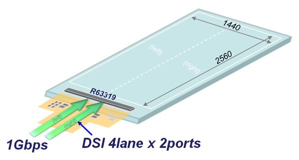
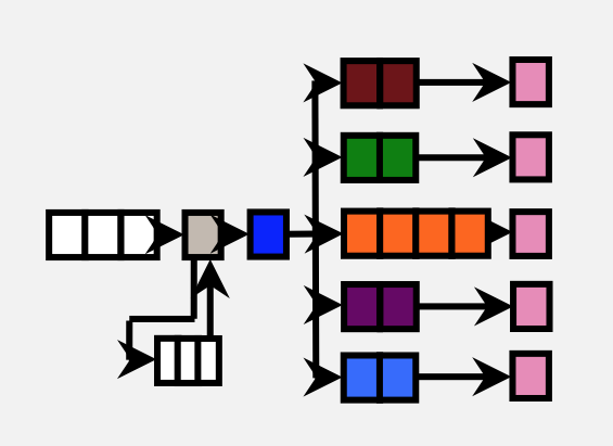
Image courtesy of Synaptics/Renesas (source)
The Qualcomm S805 uses two DSI ports with 4 lanes each to drive the display in halves of 720x2560 pixels, while the Exynos SoCs since the 5420 are able to make do with just a single 4-lane port with help of Mobile Image Compression. MIC compresses the data stream and thus avoids this bandwidth bottleneck. The disadvantage here is that the display driver itself must be able to decompress the stream.
With Samsung developing their own AMOLED display drivers they can however take advantage of this vertical integration and implement this in their phones and tablets. The power advantages here can vary up to 150mW if the image stream is able to be highly compressed, or about 100mW on average. This of course has the biggest impact on highly dynamic content, as static content power consumption has mostly been resolved by Panel Self Refresh, which has seen wide adoption over the last 18 months.
20nm Manufacturing Process
Both Samsung Semiconductor and TSMC delivered their first 20nm products in Q3 2014, but they don't represent the same jump in efficiency. Samsung's 28nm HKMG process varied a lot from TSMC's 28nm HPM process. While Samsung initially had a process lead with their gate-first approach when introducing 32nm HKMG and subsequently the 28nm shrink, TSMC went the route of gate-last approach. The advantage of the gate-last approach is that it allows for lower variance in the manufacturing process and being able to allow for better power characteristics. We've seen this as TSMC introduced the highly optimized HPM process in mobile. Qualcomm has been the biggest beneficiary as they've taken full advantage of this process jump with the Snapdragon 800 series as they moved from 28nm LP in previous SoCs.
In practical terms, Samsung is brought back on even terms with TSMC in terms of theoretical power consumption. In fact, 28nm HPM still has the same nominal transistor voltage as Samsung's new 20nm process.
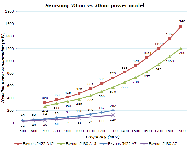
Luckily Samsung provides useful power modeling values as part of the new Intelligent Power Allocation driver for the 5422 and 5430 so we can get a rough theoretical apples-to-apples comparison as to what their 20nm process brings over the 28nm one used in their previous SoCs.
I took the median chip bin for both SoCs to extract the voltage tables in the comparison and used the P=C*f*V² formula to compute the theoretical power figure, just as Samsung does in their IPA driver for the power allocation figures. The C coefficient values are also provided by the platform tables.
We can see that for the A15 cores, there's an average 24% power reduction over all frequencies, with the top frequencies achieving a good 29% reduction. The A7 cores see the biggest overall voltage drop, averaging around -125mV, resulting in an overall 40% power reduction and even 56% at the top frequency. It's also very likely that Samsung has been tweaking the layout of the cores for either power or die size; we've seen this as the block sizes of the CPUs have varied a lot between the 5410, 5420 and 5422, even though they were on the same process node.
While these figures provide quite a significant power reduction by themselves, they must be put into perspective with what Qualcomm is publishing for their Krait cores. The Snapdragon 805 on a median speed bin at 2.65GHz declares itself with a 965mW power consumption, going down to 57mW at 300MHz. While keeping in mind that these figures ignore L2 cache power consumption as Qualcomm feeds this on a dedicated voltage rail, it still gives us a good representation of how efficient the HPM process is. The highest voltages on the S805 are still lower than the top few frequencies found on both the 5430 and the 5433.
20nm does bring with itself a big improvement in die size. If we take the 5420 as the 28nm comparison part and match it against the 5430, we see a big 45% decrease on the A7 core size, and an even bigger 64% reduction on the A15 core size. The total cluster sizes remain relatively conservative in their scaling while shrinking about 15%; this is due to SRAM in the caches having a lower shrinking factor than pure logic blocks. One must keep in mind that auxiliary logic such as PLLs, bus interfaces, and various other small blocks are part of a CPU cluster and may also impact the effective scalability. Samsung also takes advantage of artificially scaling CPU core sizes to control power consumption, so we might not be looking at an apples-to-apples comparison, especially when considering that the 5430 is employing a newer major IP revision of the CPU cores.
| Exynos 5420 vs Exynos 5430 block sizes | ||||
| Exynos 5420 | Exynos 5430 | Scaling Factor | ||
| A7 core | 0.58mm² | 0.4mm² | 0.690 | |
| A7 cluster | 3.8mm² | 3.3mm² | 0.868 | |
| A15 core | 2.74mm² | 1.67mm² | 0.609 | |
| A15 cluster | 16.49mm² | 14.5mm² | 0.879 | |
The Mali T628 between the 5420 and the 5430 actually had an increase in die size despite the process shrink, but this is due to a big increase in the cache sizes.
Samsung regards their 20nm node as very short-lived and the 5430 and 5433 look to be the only high volume chips that will be coming out on the process as their attention is focused on shipping 14nm FinFET devices in the next few months. In fact at the Samsung Investor Forum 2014 they announced mass production of a new high-end SoC has already begun mid-November and will be ramping up to full volume in early 2015. I suspect this to be the Exynos 7420 as that is the successor SoC to the 5433.
All in all, the argument that this 20nm chip should be more power efficient than the competitors' 28nm is not completely factual and doesn't seem to hold up in practice. The process still seems young and unoptimized compared to what TSMC offers on 28nm.
Before we get to the performance and power figures, I'm handing things over to Ryan as we take a look at the architectural changes, starting with an analysis of the Cortex A53.
Cortex A53 - Architecture
As the owners and creators of the ARM instruction set architecture, ARM (the company) is in an interesting place with regards to both CPU and ISA development. Unlike any other ISA architect, ARM both designs CPUs off of their ISA and licenses that ISA out to other companies as well, creating a marketplace where ARM is both a master and a competitor all at once. From a financial perspective ARM wins either way – architecture licensees pay royalties as well as CPU licensees – but it means that ARM’s CPU designs are by no means a shoe-in, especially at the lucrative high-end of the market.
At the same time the forward-looking nature of ARM’s licensing business means that we get to see their hand well before anyone else’s, as ARM’s licensing model is based around announcing their in-house Cortex CPU designs years in advance to attract customers. Quite often we will know what ARM’s CPU designs are months (or years) before we know what their competition will be. Case in point, for ARMv8 ARM announced their Cortex A53 and Cortex A57 designs over 2 years ago, meaning that although the A53 and A57 product designations are well known, it’s only now that we truly get to see the fruits of ARM’s labor in the consumer market.
At the small end of ARM’s ARMv8 processor lineup is the A53. The successor to the A7, the A53 embodies the same incredibly low power, small die size, and moderate performance goals of the A7 while extending the architecture to 64-bits, as well as working in some further performance improvements. A7 was popular on its own in lower-end Android devices, and for A53 we expect the situation to be much the same. However for the purpose of Exynos, its calling will be as the LITTLE half of its big.LITTLE configuration to drive the SoC during low-performance circumstances.
As with A7, A53 is an in-order design, which in some ways makes it the more interesting of the two ARMv8 designs out of ARM. While A57 gets a comparatively huge die size and power budget to implement high performance features, A53 gets little power, little die size, and ultimately has to get whatever performance it can out of in-order execution. With out-of-order execution being prohibitively expensive in die space and power for A53, this puts ARM in the position of trying to optimize an in-order design as far as they can, explicitly without making the jump to Out-of-Order Execution (OoOE).
Peter Greenhalgh, lead architect of the A53, had a few words to say on the design goals of A53 while taking questions as a guest late last year in a Q&A session here at AnandTech:
Cortex-A53 has the same pipeline length as Cortex-A7 so I would expect to see similar frequencies when implemented on the same process geometry. Within the same pipeline length the design team focused on increasing dual-issue, in-order performance as far as we possibly could. This involved symmetric dual-issue of most of the instruction set, more forwarding paths in the data-paths, reduced issue latency, larger and more associative TLB, vastly increased conditional and indirect branch prediction resources, and expanded instruction and data prefetching. The result of all these changes is an increase in SPECInt-2000 performance from 0.35-SPEC/MHz on Cortex-A7 to 0.50-SPEC/MHz on Cortex-A53. This should provide a noticeable performance uplift on the next generation of smartphones using Cortex-A53.
At its core, the A53 retains the same execution characteristics of the A7. This means we’re looking at a dual-issue in-order CPU with a nice and short 8-stage pipeline. This is coupled with a variable amount of both L1 data cache and L1 instruction cache, ranging from 8KB to 64KB each. L2 cache meanwhile is optional and similarly variable from 128KB to 2MB – Exynos 5433 uses 512KB 256K of the stuff – with there being a single, wide interface between the entire collection of A53 cores and the L2 cache, allowing each core to access the L2 in sequence.
| ARM CPU Core Comparison | ||||||
| Cortex-A7 | Cortex-A53 | |||||
| ARM ISA | ARMv7 (32-bit) | ARMv8 (32/64-bit) | ||||
| Issue Width | 2 micro-ops | 2 micro-ops | ||||
| Pipeline Length | 8 | 8 | ||||
| Integer Add | 2 | 2 | ||||
| Integer Mul | 1 | 1 | ||||
| Load/Store Units | 1 | 1 | ||||
| Branch Units | 1 | 1 | ||||
| FP/NEON ALUs | 1x64-bit | 1x64-bit | ||||
| L1 Cache | 8KB-64KB I$ + 8KB-64KB D$ | 8KB-64KB I$ + 8KB-64KB D$ | ||||
| L2 Cache | 128KB - 1MB (Optional) | 128KB - 2MB (Optional) | ||||
For A53, ARM has opted to focus on improving the processor at every stage in order to improve the performance of its dual-issue design. Of these changes, the biggest changes are in the dual-issue capabilities of the processor itself, along with changes to branch prediction.
In the case of dual-issue capabilities, ARM has increased the types of operations that can be issued from the second instruction slot, slot-1. With A7 slot-0 was full-featured while slot-1 could only issue branch and integer data; now for A53, slot-1 can also issue load-stores and FP/NEON operations, bringing it up to parity with slot-0. This means that as far as dual-issue conditions go, A53 should now only be limited by available execution units and whether the next operation can safely be co-issued.
Meanwhile for branch prediction, ARM has worked on beefing up A53’s branch unit to improve the hit rate and otherwise reduce the time wasted on mispredicted branches. Here A53 gains new conditional and indirect predictors, with the conditional predictor being a 6Kbit gshare predictor, while the indirect predictor can hold 256-entries with path history.
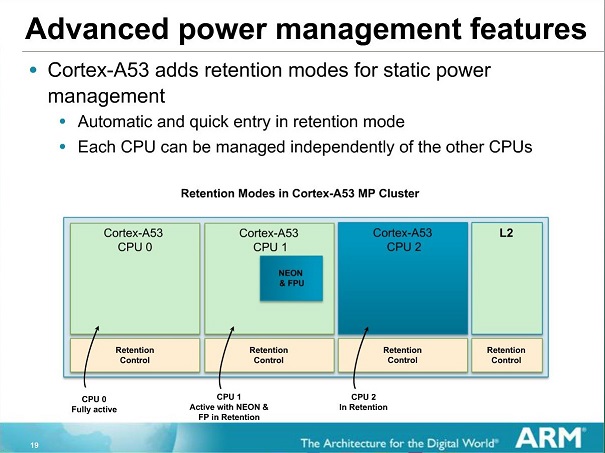
Elsewhere, when it comes to power, the A53 has an optional new ability to better switch between power states. The new architecture adds new retention states that are able to power-gate individual blocks of the CPU core, such as for example the NEON unit, and provide lower latency power-gating idle states.
As far as performance goes, ARM tells us that A53 can match A9 in performance at equivalent clock speeds. Given just how fast A9 is and just how small A53 is, to be able to match A9’s performance while undercutting it in die size and power consumption in this manner would be a feather in ARM’s cap, and an impressive follow-up to the A8-like performance of A7.
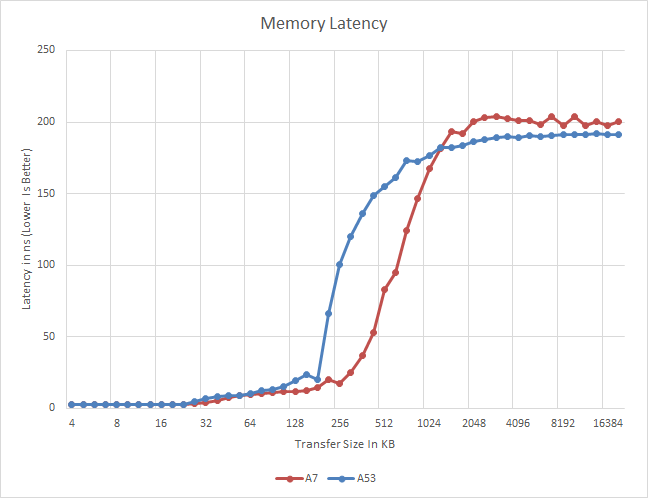
Meanwhile a quick look at some of our synthetic tests finds that the A53 cores in the Exynos 5433 are doing unusually poorly in latency compared the A7 cores, despite the fact that both parts have 512KB 256K of L2 cache. We have other reasons to believe the 5433 has 512KB of L2 cache for the A53 cores,* but looking at this you wouldn't think so, as latency shoots up much earlier, making it seem as if the chip has only 256KB of cache.
* Correction 24/03/2015: Our initial info of 512K L2 cache on the A53 cluster was incorrect and has henceforth been edited to 256K as published by Samsung. (Source)
Given the new information, it looks like the A53 is behaving as it should and the anomaly we saw in the data is actually a proper representation of the real-world scenario.
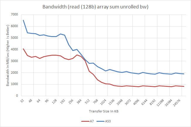
Switching from latency to read bandwidth, we find an interesting outcome for the A53 in the Exynos 5433: memory bandwidth, a lot of it. Truth be told I'm still scratching my head at this one; it's not clear whether this is a result of the dual-issue improvements, something Samsung did for 5433, both, or something else entirely. But the A53 cores in the 5433 have roughly twice as much memory bandwidth as the A7 cores in 5430. This is the case both inside the cache areas and outside to main memory, which points to some greater factor at work here.
Finally, it’s interesting to note at this point that after taking care of the dual-issue bottlenecks on A53, ARM has come very close to pushing a dual-issue in-order design as far as they can go. With most instructions executing in 1 cycle, A53 executes as wide a variety of instructions as quickly as it can, and consequently improving branch prediction is one of the few avenues left for further improving performance. This may partially explain why ARM has already announced the A57’s successor for a couple of years down the line – A72 – but has not announced an A53 successor. Short of going wider or OoOE, I would be curious to see what ARM does after A53.
Cortex A53 - Synthetic Performance
Usually big.LITTLE HMP designs have all their cores online and available to the system, and migrate a more demanding process to the big cores only when necessary. This poses a problem for us when trying to isolate the performance of the little cores.
Initially I was unable to turn off the cores via traditional methods such as simply hot-plugging the CPU cores, a method I used on Huawei's HiSilicon Kirin 920 for example. This caused a bit of a headache and I had to circumvent this by taking advantage of the Global Task Scheduling parameters of the kernel to block off any processes migrating over to the big cluster and enabling forceful down-migration on any entity that is forked on the big CPUs.
Later on, I finally found which mechanism was preventing me from turning off the cores properly - one of Samsung's own power management drivers that serves to hot plug cores when turning the screen off was keeping me from turning a CPU off while the screen was on. I disabled this driver at a later date after doing the performance and initial power measurement, and I re-verified and checked that my numbers were still valid, which luckily they were.
For starters, we turn to SPECint2000. Developed by the Standard Performance Evaluation Corporation, SPECint2000 is the integer component of their larger SPEC CPU2000 benchmark. Designed around the turn of the century, officially SPEC CPU2000 has been retired for PC processors, but mobile processors are roughly a decade behind their PC counterparts in performance. Keeping that in mind it still provides an excellent benchmark for today's mobile phones and allows us to do single-threaded architectural comparisons between the competing CPU designs out there.
I'd also like to mention that we're still working with an ARMv7 version of the benchmark and thus it doesn't fully take advantage of the Exynos 5433's ARMv8 cores, even though it's limited to AArch32 by software for now.
| SPECint2000 - Estimated Scores | ||||||
| Exynos 5430 (A7) |
Exynos 5433 (A53) |
% Advantage | ||||
| 164.gzip | 686 | 814 | 19% | |||
| 175.vpr | 292 | 272 | -7% | |||
| 176.gcc | 431 | 597 | 39% | |||
| 177.mesa | 505 | 633 | 25% | |||
| 179.art | 225 | 523 | 132% | |||
| 181.mcf | 202 | 291 | 44% | |||
| 186.crafty | 342 | 448 | 31% | |||
| 197.parser | 321 | 348 | 8% | |||
| 252.eon | 677 | 935 | 38% | |||
| 253.perlbmk | 393 | 529 | 35% | |||
| 254.gap | 395 | 544 | 38% | |||
| 255.vortex | 427 | 529 | 24% | |||
| 256.bzip2 | 344 | 362 | 5% | |||
| 300.twolf | 302 | 284 | -6% | |||
We're comparing the A7 in the Exynos 5430 versus the A53 in the Exynos 5433. Here we see an overall increase of 30% for the A53 cores. Both SoCs run the little clusters at the same frequency and thus it gives us a direct IPC comparison between the two architectures.
The biggest outlier here is the ART test, which is an image recognition / neural network workload that tests floating point rather than integer performance. There are also drops in performance on the VPR and TWOLF tests, which may be running into the L2 cache performance issues discussed on the previous page.
Our other synthetic performance benchmark is GeekBench 3. Here we're able to take advantage of at least the AArch32 mode of the CPU, which has a big impact on the crypto scores:
| GeekBench 3 - Integer Performance | ||||||
| A7 (ARMv7) | A53 (AArch32) | % Advantage | ||||
| AES ST | 23.1 MB/s | 662 MB/s | 1865% | |||
| AES MT | 89.4 MB/s | 2570 MB/s | 1874% | |||
| Twofish ST | 26.9 MB/s | 45.9 MB/s | 70% | |||
| Twofish MT | 101.8 MB/s | 277.2 MB/s | 172% | |||
| SHA1 ST | 53.9 MB/s | 281.2 MB/s | 421% | |||
| SHA1 MT | 210.8 MB/s | 1880 MB/s | 791% | |||
| SHA2 ST | 30.1 MB/s | 69.6 MB/s | 131% | |||
| SHA2 MT | 115.8 MB/ | 330.6 MB/s | 185% | |||
| BZip2Comp ST | 1.95 MB/s | 2.09 MB/s | 7% | |||
| BZip2Comp MT | 5.52 MB/s | 11.7 MB/s | 111% | |||
| Bzip2Decomp ST | 2.83 MB/ | 3.24 MB/s | 14% | |||
| Bzip2Decomp MT | 7.41 MB/s | 14.0 MB/s | 89% | |||
| JPG Comp ST | 6.84 MP/s | 9.95 MPs | 45% | |||
| JPG Comp MT | 26.2 MP/s | 59.5 MP/s | 127% | |||
| JPG Decomp ST | 11.4 MP/s | 14.3 MP/s | 25% | |||
| JPG Decomp MT | 43.1 MP/s | 72.0 MP/s | 67% | |||
| PNG Comp ST | 0.51 MP/s | 0.591 MP/s | 16% | |||
| PNG Comp MT | 1.28 MP/s | 2.49 MP/s | 94% | |||
| PNG Decomp ST | 7.35 MP/s | 9.68 MP/s | 31% | |||
| PNG Decomp MT | 25.2 MPs | 39.2 MP/s | 55% | |||
| Sobel ST | 18.2 MP/s | 22.0 MP/s | 21% | |||
| Sobel MT | 67.7 MP/s | 103.8 MP/s | 53% | |||
| Lua ST | 0.469 MB/s | 0.579 MB/s | 23% | |||
| Lua MT | 1.42 MB/s | 1.75 MB/s | 23% | |||
| Dijkstra ST | 2.31 Mpairs/s | 2.84 Mpairs/s | 23% | |||
| Dijkstra MT | 6.7 Mpairs/s | 11 Mpairs/s | 64% | |||
Due to new cryptographic instructions in the ARMv8 ISA we see huge improvements in the AES and SHA tests, not too different from the increase we saw when Apple introduced the A7 in the iPhone 5S. However, if we disregard the crypto benchmarks, we see a more reasonable but still very impressive average improvement of 49% across the rest of the benchmarks. Only the BZip compression and decompression tests show only minor improvement in their single-threaded runs, which oddly enough were not reproduced in the multi-threaded runs.
| GeekBench 3 - Floating Point Performance | ||||||
| A7 (ARMv7) | A53 (AArch32) | % Advantage | ||||
| BlackScholes ST | 1.68 Mnodes/s | 2.12 Mnodes/s | 26% | |||
| BlackScholes MT | 6.53 Mnodes/s | 12.9Mnodes/s | 97% | |||
| Mandelbrot ST | 448.6 MFLOPS | 519.7 MFLOPS | 15% | |||
| Mandelbrot MT | 1.75 GFLOPS | 3.44 GFLOPS | 96% | |||
| Sharpen Filter ST | 305.5 MFLOPS | 607.2MFLOPS | 99% | |||
| Sharpen Filter MT | 1.17 GFLOPS | 2.69 GFLOPS | 129% | |||
| Blur Filter ST | 0.365 GFLOPS | 0.488 GFLOPS | 33% | |||
| Blur Filter MT | 1.44 GFLOPS | 2.95 GFLOPS | 11% | |||
| SGEMM ST | 0.601 GFLOPS | 0.577 GFLOPS | 104% | |||
| SGEMM MT | 0.869 GFLOPS | 3.78 GFLOPS | 339% | |||
| DGEMM ST | 0.234 GFLOPS | 0.239 GFLOPS | 2% | |||
| DGEMM MT | 0.578 GFLOPS | 2.52 GFLOPS | 342% | |||
| SFFT ST | 0.318 GFLOPS | 1.22 GFLOPS | 283% | |||
| SFFT MT | 1.27 GFLOPS | 4.89 GFLOPS | 285% | |||
| DFFT ST | 215.3 MFLOPS | 919.8 MFLOPS | 327% | |||
| DFFT MT | 0.758 GFLOPS | 3.01 GFLOPS | 297% | |||
| N-Body ST | 147.1 Kpairs/s | 381.4 Kpairs/s | 159% | |||
| N-Body MT | 0.504 Mpairs/s | 1.54 Mpairs/s | 205% | |||
| Ray Trace ST | 0.598 MP/s | 1.72 MP/s | 187% | |||
| Ray Trace MT | 2.30 MP/s | 7.24 MP/s | 214% | |||
In the floating point performance benchmarks we again see massive improvements, with many scores being twice or even three times the performance of the A7. Again there's a peculiarity in that the multi-threaded scores show a higher improvement over the A7 than the single-threaded tests.
Power Consumption
Testing out power consumption on the little cores was a bit tricky as I needed to remain on the little clusters without spilling over four threads that might wake up the big cores. For this, I use hot-plugging to disable the cores that we're not measuring directly to avoid any power overhead caused by unwanted activity that might occur on the big cluster.
To get to these figures, I derived the power numbers by measuring total energy consumption during each test for a 1 minute period and repeated this several times to ensure the accuracy of the numbers. Power of the screen has also been subtracted via the same methodology and verified that it is accurate enough to give a pure representation of the load power of the SoC only. On both devices the GPU and display pipeline are power-gated and as such the load power should consist primarily of the regulator overheads, CPU cores, L2 caches, system memory and interconnect bus interfaces.
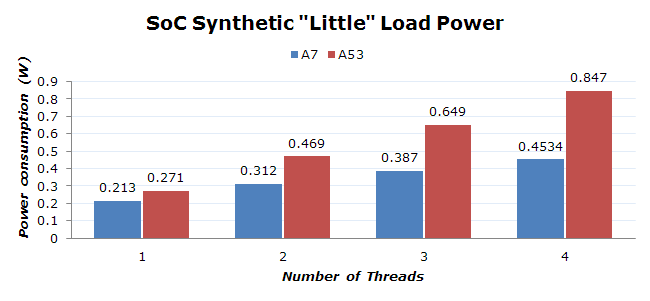
When loading a various number of threads on the little cluster we see some interesting numbers when comparing the 5430 to the 5433. First of all, it's obvious that the A53 is more power hungry than the A7. The surprise is that this factor seems to be quite big. For the A7, we see a base 213mW system load power when firing up one thread, with decreasing increments for each additional thread. We see 99, 75, and 66 mW additional power for the added threads.
I'm not quite sure why the numbers are diminishing here - I first thought that the scheduler would've been fast enough to try to fill the cores' capacity causing each additional core to have more idle time to itself since we're targeting a 96% load per thread. But that's not the case, as each thread was on its own core and the load was evenly distributed.
Looking at the A53, we see a similar story but with inflated figures. The base 271mW load power with one thread is a tad higher for the new ARMv8 cores than for the A7, and that difference gets bigger with each additional thread we run.
Initially I had tested these figures without shutting down the cores individually, and used the HMP scheduler controls to isolate the big cluster, which led me to the further investigations in the scheduler. It seems that the current GTS implementation delivered on these devices is still lacking a feature called "Small Task Packing". Small task packing allows the scheduler to try and pack low-load tasks onto an already woken up CPU core instead of spreading the load throughout the cores of the cluster.
In case of the current big.LITTLE implementations, spreading loads throughout the cluster is a disadvantageous strategy as it forces cores to come out of their independent power collapse states on a frequent basis. I'm not sure if that's why we're seeing diminishing power consumption numbers with increased thread count; the low-thread power numbers may be inflated by rogue idle wake-ups on the what should have been remaining idle cores. This delta decreases as we increase thread count and thus CPUs which are awake, so this would be a sensible explanation of the effect.
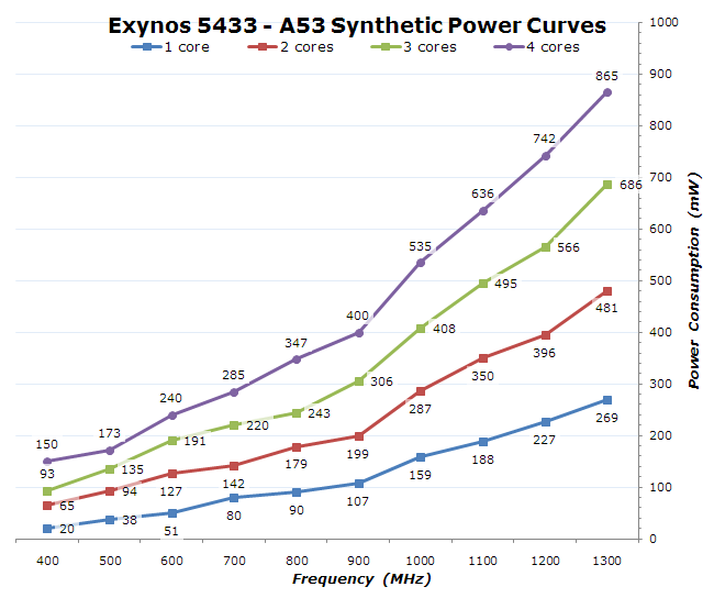
To verify this I re-ran a full power analysis on the full frequency curve of the CPU while isolating the cores via hot plugging. This should avoid any incorrect measurements that would have occurred by the other method.
The effect is repeated here too, but only the highest frequency of the A53, it was harder to notice on the lower frequencies. The interesting thing about the curves to notice is that power goes up by a relatively large amount after the 1GHz P-state. This also correlates with a higher voltage bump from 962.5mV on the 900MHz state to 1025mV and up at higher frequencies.
What we're left with is a rough estimate of per-core power load for both the A7 and the A53 at their highest frequencies of 1300MHz. I calculated this number by trying to account for the cluster power overhead and just look at the power of the cores themselves:
| Estimated Little Per-Core Power Consumption | |||
| A7 (Exynos 5430) | A53 (Exynos 5433) | Increase | |
| Little per-core load | ~85mW | ~189mW | 122% |
I think it's safe to say the A53 consumes a little over twice the power of an A7 core given almost the same SoC platform. This seems a lot given the actual performance increase is much less than that; it would mean that the performance/Watt (perf/W) has actually gone down with the A53. We also have to keep in mind that the A53 adds a lot of new silicon to the die, so let's look at the block sizes between the A7 and the A53:
| A7 vs A57 Block Sizes | ||||
| A7 (Exynos 5430) | A53 (Exynos 5433) | Scaling Factor | ||
| Core | 0.40mm² | 0.70mm² | 1.75 | |
| Cluster | 3.30mm² | 4.58mm² | 1.38 | |
While still maintaining rather minuscule core sizes of under 1mm², the A53 is still 1.75 times bigger than an A7 core on the same process node. The total cluster size difference comes in at a lesser 1.38x factor, but that is because the cache sizes have remained the same between the two implementations.
To try to actually measure a realistic and real-world scenario of perf/W, I tried hard to find a good test-load. After some searching around and trying out various items from our benchmark suite, I ended up focusing on BaseMark OS II's XML sub-test. The test is a good candidate because it offers a scaling load with three threads that put both a high load on some cores and let others exercise their power management states at the same time, definitely behavior you would see in day-to-day applications.
| BaseMark OS II - XML Parsing Energy Efficiency | ||||
| Performance | Energy | Performance/Energy | ||
| A7 (Exynos 5430) | 77.93MB/s | 10.56mWh | ~7.38 | |
| A53 (Exynos 5433) | 109.36MB/s | 17.11mWh | ~6.39 | |
Indeed we see that the A53 is able to achieve greater performance than the A7, but at a greater added cost of energy than the performance increase itself. The effect is that the overall perf/W went down by 15% in this particular test. This is an interesting metric as it validates the continued existence of standalone A7 SoCs over A53 designs, with the new A53 cores being something like an extension to the perf/W curve.
All in call, I think ARM made the right choices here with the A53. The performance increases were definitely needed - not only for standalone SoCs which rely solely on the A53, but also for big.LITTLE SoCs. What I hope to see in the future is more aggressively clocked A53 implementations going beyond the 1.5-1.7GHz that we currently see as the upper limits in SoCs such as the Snapdragon 810 and the Snapdragon 615. The question is whether clock increases and coming upgrades to the memory systems such as the introduction of LPDDR4 memory next year will be enough to keep the core competitive. I certainly hope, and think so.
While we have a good impression of the A53 cores, actual high-end performance is delivered by the A57 cores. So let's have a look and repeat our exercise for the A57.
Cortex A57 - Architecture
Shifting gears to a look at the Exynos 5433’s high-performance CPU cores, we have the Cortex-A57, the successor to ARM's earlier ARMv7 Cortex-A15.
As ARM’s first high-performance ARMv8 core, A57 is jumping into an interesting market. A57’s first year is likely to be even more successful than A15 was, and yet this is going to be the most competitive landscape yet within the ARM ecosystem, thanks to a larger number of ARM architecture licensees than ever before. Many of these licensees are in the server realm – companies like AppliedMicro who are making a run at the server market – meanwhile others such as Apple and NVIDIA have used their designs in the consumer market, even beating out A57 by nearly a year in the case of Apple. Still, within the narrower confines of the Android space, A57 is currently the CPU to beat for 2015, with everyone from Samsung to Qualcomm licensing the design for their high-end CPUs.
Diving into A57 itself then, A57 is in many ways a direct evolution and continuation of the A15 design. Intended for 28nm and newer nodes, A57 essentially picks up where A15 left off, introducing ARMv8 support while further ramping up ARM's IPC, overall single-threaded performance, and even energy efficiency. Under the hood ARM has made a number of changes to improve efficiency while retaining other elements of A15 that still make sense. The end result is something akin to an Intel “tock”, meaning we’re looking at something that isn’t a massive overhaul of the architecture (e.g. Cyclone or Denver) but institutes a number of new features and optimizations.
A57 is at its heart a fully out-of-order design, making for a very interesting contrast to NVIDIA’s Denver, which we took a look at last week. This basically being the norm to NVIDIA’s unorthodoxy, A57 is a much more traditional CPU design that follows ARM’s historical design tendencies and is similarly intended to fit in roughly the same design envelope as A15.
From a high-level perspective, ARM makes a fairly straightforward tradeoff in terms of performance and power consumption. A57 is designed to be bigger and more performant than A15, but in turn it can consume more power as well. ARM’s internal projections for A57 are that it can achieve 25-50% better IPC at a cost of 20% higher power consumption if built on the 28nm node. In terms of overall energy efficiency this should leave A57 with a decent edge over A15, thanks to performance increases outpacing the power consumption increase.
The wildcard factor in all of this will be the manufacturing node, especially the temperamental 20nm processes. While A57 can be produced on 28nm, in keeping with the pace of manufacturing technology and the need to offset its larger size, the first consumer A57 designs like the Exynos 5433 are being produced at 20nm, as opposed to 28nm for the bulk of A15 designs. The smaller process helps to keep the size of A57 relatively small – enough to easily fit four cores on an SoC – and it means that we’re getting the power efficiency gains that come from a smaller process node, adding to A57’s architectural gains. However it also means that the performance gains on shipping A57 SoCs are going to be influenced by manufacturing factors such as leakage and the viability of higher clock speeds, so the real-world performance gains over A15 are going to be a bit more variable. Overall ARM is pushing for a higher IPC design in part to better control these factors, as higher IPC designs would allow for partners to ramp down the clock speeds a bit, and thereby voltage and power consumption.
In any case, let’s talk about the design of the A57. In creating the A57, ARM tells us that their goal was to design the CPU around the kinds of compute workloads they expect to see over the next few years, in order to get the best real-world performance out of their design. To that end, ARM says that in planning A57 they found that mobile workloads aren’t as instruction pipeline sensitive as they once were, and as a result the biggest bottlenecks aren’t in the pipeline itself but rather in feeding the pipeline. Consequently, A57’s design has made fewer changes to the A15 pipeline and focused more on improving the hardware supporting the pipeline, such as fetch, decode, and out-of-order execution capabilities.
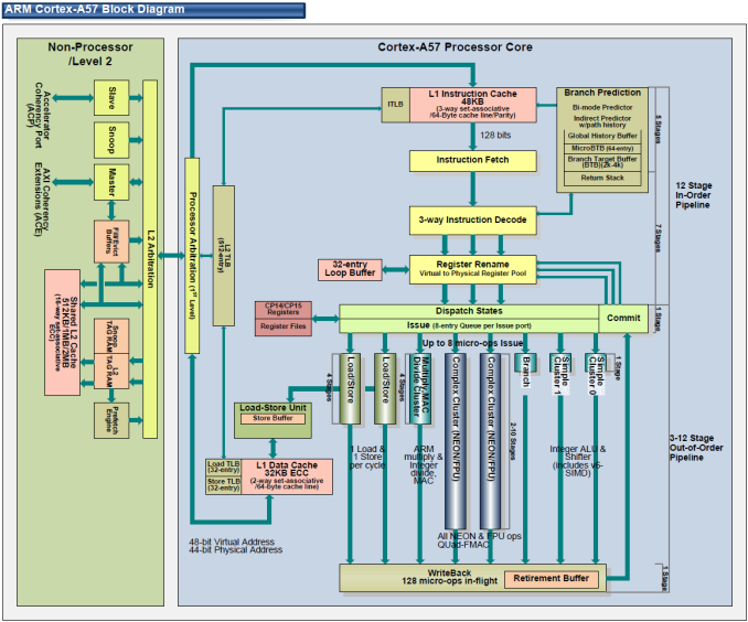
Image courtesy of Hiroshige Goto
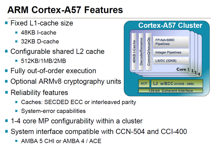
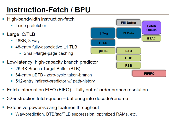
Starting at the front then, at the fetch stage ARM has made numerous small changes. The L1 cache has been expanded from 32KB in A15 to 48KB in A57, and similarly its associativity has gone from 2-way to 3-way. The overall increase in cache helps to improve performance, though perhaps more importantly the larger instruction cache helps to offset the larger size of the 64-bit ARM instructions. Meanwhile the Branch Target Buffer, used to store past branches and better predict future branches, has seen its size doubled entirely, now coming in at 2K-4K. Meanwhile on the data side the L1 data cache is left unchanged at 32KB.
L2 cache on the other hand is configurable on a per-SoC basis. A57 supports L2 cache sizes between 512KB and 2MB, with the cache being 16-way set-associative. Each A57 core gets its own interface to the L2 cache, so there is no bandwidth sharing at the interface level. It also bears mentioning at this point that with A57 ARM now supports multiple memory page sizes on top of the standard 4K memory page size, though the larger pages are primarily for server use.
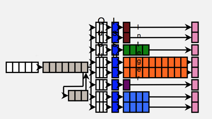
For instruction decoding, A57 retains the familiar 3-wide decoder front-end. ARM always faces a fine balancing act on decoder size – wider decoders are physically larger – and as with A57 this falls in line with ARM’s goal to focus on feeding the pipeline as opposed to the pipeline itself, as ARM believes they are not yet at the limit of a 3-wide pathway. Though not wider, the decoder has seen other changes to improve performance and power efficiency. Of particular note, the various decode planes for each instruction set – Thumb, NEON, AArch64, and ARMv7 – can now be power gated so that only the decode plane necessary is powered up, helping to offset the cost of needing to support four different instruction formats. Register renaming has also been tweaked at the decode stage, particularly to take advantage of the fact that ARMv8 allows for a flat register map, as opposed to the earlier banked register map.
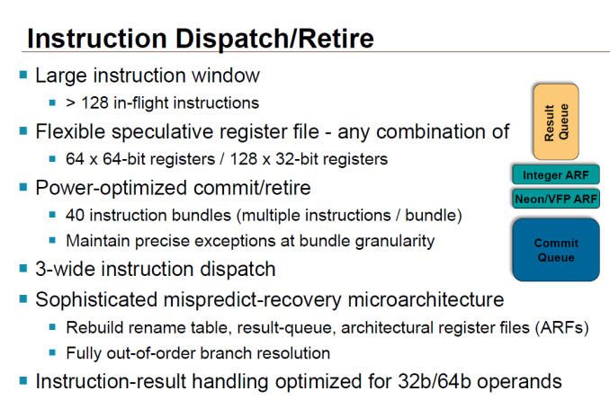
Meanwhile ARM has also made a few important changes at the instruction dispatch and execution stage. Of note, the instruction window for OoOE has once again been increased in size; ARM still isn’t commenting on the precise size, but it is said to be able to hold more than 128 instructions to further improve OoOE performance. Elsewhere the register file has been given its own enhancements, primarily for AArch64 compatibility. Each 4K segment of the register file can now be configured as 128 32-bit registers or 64 64-bit registers, allowing for relatively small portions of the file to be switched over to 64-bit mode and avoiding wasting space on values that don’t require the larger register format.
| ARM CPU Core Comparison | ||||||
| Cortex-A15 | Cortex-A57 | |||||
| ARM ISA | ARMv7 (32-bit) | ARMv8 (32/64-bit) | ||||
| Decoder Width | 3 micro-ops | 3 micro-ops | ||||
| Pipeline Length | 18 stages | 18 stages | ||||
| Branch Mispredict Penalty | 15 cycles | 15 cycles? | ||||
| Integer Add | 2 | 2 | ||||
| Integer Mul | 1 | 1 | ||||
| Load/Store Units | 1 + 1 (Dedicated L/S) | 1 + 1 (Dedicated L/S) | ||||
| Branch Units | 1 | 1 | ||||
| FP/NEON ALUs | 2x64-bit | 2x128-bit | ||||
| L1 Cache | 32KB I$ + 32KB D$ | 48KB I$ + 32KB D$ | ||||
| L2 Cache | 512KB - 4MB | 512KB - 2MB | ||||
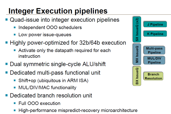
As for the pipeline itself, both the integer and floating point units have seen some upgrades for performance and 64-bit compatibility reasons. Though ARM doesn’t go into great detail on how they have this arranged, they have integer datapaths for both 32-bit and 64-bit execution, allowing them to only fire up the 64-bit path when they need it. Additional paths do create some complexity, but the pay-off over a single 64-bit path is that additional transistors are not fired up and additional power burnt just to run 32-bit code.
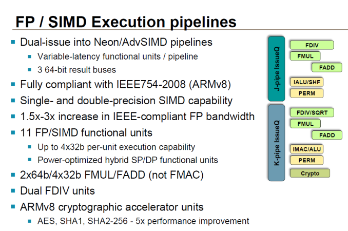
The floating point/NEON units on the other hand are outright wider, doubling from 64-bits to 128-bits and in turn potentially doubling NEON performance (when the FP units can be fully fed). Unlike the integer pipeline there aren’t separate paths for different data sizes, but ARM does tell us that they have worked in some further power optimizations to keep power usage down. These units are now also IEEE-754-2008 compliant when executing ARMv8 code. For the consumer market this does not have much of an impact, but it is an important distinction for the server market, which is another area ARM is hoping to get the A57 into now that they have 64-bit addressing capabilities. Finally, A57 supports an optional cryptography accelerator unit at this stage to speed up AES and SHA1/SHA2-256 performance.
Last but certainly not least, the load/store units have learned a few new tricks as well. Loads can now bypass non-disambiguated stores, which is good for around another 5% increase in performance. At the same time a dependence predictor is now in place at this stage, primarily to help improve OoOE performance by preventing A57 from over-speculating and otherwise harming performance during speculative memory operations.
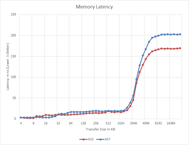
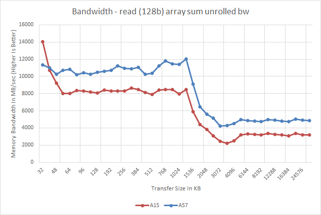
Meanwhile a quick look at memory latency and bandwidth on the A57 cores in the Exynos 5433 finds an unexpected pairing. Latency is virtually unchanged from the A15 through the L2 cache, but once it hits main memory the latency increases by nearly 40ns. On the other hand memory bandwidth is consistently better on the A57, even in cache. As far as latency is concerned this may be due to a Samsung design decision in the SoC itself. Meanwhile the improved bandwidth is likely a consequence of A57's various enhancements to improve throughput within the CPU cores.
ARM's relatively poor memory bandwidth figures have garnered them a poor reputation when it comes to memory performance, but what we are seeing here might be a gross misrepresentation of real-world performance. To understand how these figures come to be, we need to look at how the CPU is wired to the SoC's interconnect and memory controllers. ARM, as opposed to designs by Apple or NVIDIA, uses separate read and write data-ports in its fabric. On the cluster level, this is a dual 128-bit interface (one for reads, one for writes) that connects to matching ports of the SoC's memory controllers via the CCI's (Cache Coherent Interconnect) crossbar architecture. On the Exynos 5430 and 5433, the CCI runs at half the DRAM frequency, meaning 412.5 MHz for the aforementioned SoCs. This results in a maximum physical bandwidth of 6.6 GB/s in each direction.
What most of today's synthetic benchmarks portray is only the bandwidth measured in either direction, giving ARM a distinctive disadvantage. Total achievable bandwidth can reach double these figures. In fact, when we execute simultaneous read and write tests (multithreaded on two CPUs) we benchmark bandwidth numbers reaching the theoretical peaks of the memory controllers at 13.2GB/s. Interestingly, it seems ARM is employing the same setup to the L2 cache as bandwidth there also doubles to up to 25GB/s for the 5430's A15 and 27.5GB/s for the 5433's A57 clusters.
As to why ARM prefers this kind of configuration is a good question. We suspect that there may be power or latency advantages to the design, but we cannot be certain of it. Overall, it should have less of an impact in real-world scenarios as the benchmarks would lead one believe. Use cases where computations are either read or write heavy should only appear in scenarios such as video encoding or texture decompression such as loading video game assets, with the the former not being a real issue in the mobile space due to fixed-function hardware dedicated to the task.
Overall then, as put together A57 serves as the natural step up from A15, both in terms of the underlying design and of the overarching architecture. There is no single great change to drive performance here – and in fact the instruction pipeline isn’t much different in execution – but by focusing on building out for AArch64 execution and improvements to better feed those pipelines, ARM expects that they can get a significant IPC increase over A15. Coupled with 20nm and later 16nm/14nm processes ARM and their partners are hoping to push A57 far, though given the fact that A15 was already a bit power hungry in phones, it will be interesting to see how much of those process gains are spent on performance (clock speeds) and how much is spent on bringing down power consumption.
Meanwhile, ARM’s long-term plans for A57 also call for it to lead a double-life as a server CPU. With a 64-bit memory space, applications running on the A57 can finally address all the memory they need (and then some), so coupled with the IPC increase ARM is hoping to crack the server market in a way that early A15 efforts never did. Among the first companies shipping a server CPU will be AMD and their A1100, so it will be interesting to see how A57 plays out in the server market over the coming year.
Cortex A57 - Synthetic Performance
We once again turn to SPECint2000 for an estimated performance score of the architecture - again, keeping in mind that this a deprecated and retired benchmark on the PC space.
| SPECint2000 - Estimated Scores | ||||||
| Apple A8 | Tegra K1-64 (Denver) |
Exynos 5430 (A15) |
Exynos 5433 (A57) |
5433 > 5430 %Advantage |
||
| 164.gzip | 842 | 1269 | 703 | 813 | 15% | |
| 175.vpr | 1228 | 1312 | 782 | 1120 | 44% | |
| 176.gcc | 1810 | 1884 | 1222 | 1549 | 28% | |
| 177.mesa | 2187 | 1308 | 1666 | 28% | ||
| 179.art | 5146 | 2113 | 2574 | 24% | ||
| 181.mcf | 1420 | 1746 | 983 | 1192 | 23% | |
| 186.crafty | 2021 | 1470 | 854 | 1149 | 34% | |
| 197.parser | 1129 | 1192 | 728 | 841 | 16% | |
| 252.eon | 1933 | 2342 | 1585 | 2096 | 32% | |
| 253.perlbmk | 1666 | 1818 | 994 | 1258 | 27% | |
| 254.gap | 1821 | 1844 | 1279 | 1466 | 15% | |
| 255.vortex | 1716 | 2567 | 1283 | 1652 | 32% | |
| 256.bzip2 | 1234 | 1468 | 898 | 1027 | 15% | |
| 300.twolf | 1633 | 1785 | 1102 | 1260 | 16% | |
When we look at the results of the SPEC scores, the gains are indeed smaller than what the A53 got over the A7. We get a relatively even 25% average boost throughout the various sub-tests of SPECint2000. Considering that the Exynos 5430 ran at 1.8GHz versus 1.9GHz for the 5433, this slight advantage goes down to 18% average when normalizing for clock speeds. The 177.mesa and 179.art tests are normally not part of the SPECint2000 suite but part of SPECfp2000 (being floating points tests), and usually don't get taken into account in the integer score of SPEC.
| GeekBench 3 - Integer Performance | ||||||
| A15 (ARMv7) | A57 (AArch32) | % Advantage | ||||
| AES ST | 68.4 MB/s | 1330 MB/s | 1844% | |||
| AES MT | 267.9 MB/s | 4260 MB/s | 1490% | |||
| Twofish ST | 64.4 MB/s | 81.9 MB/s | 27% | |||
| Twofish MT | 249.6 MB/s | 440.5 MB/s | 76% | |||
| SHA1 ST | 187.6 MB/s | 464.2 MB/s | 147% | |||
| SHA1 MT | 712.2 MB/s | 2020 MB/s | 183% | |||
| SHA2 ST | 80.5 MB/s | 121.9 MB/s | 51% | |||
| SHA2 MT | 316.0 MB/ | 528.3 MB/s | 67% | |||
| BZip2Comp ST | 3.81 MB/s | 4.88 MB/s | 28% | |||
| BZip2Comp MT | 13.5 MB/s | 19.3 MB/s | 43% | |||
| Bzip2Decomp ST | 5.93 MB/ | 7.41 MB/s | 25% | |||
| Bzip2Decomp MT | 22 MB/s | 29.7 MB/s | 35% | |||
| JPG Comp ST | 14.7 MP/s | 19.3 MPs | 31% | |||
| JPG Comp MT | 60.8 MP/s | 88.8 MP/s | 46% | |||
| JPG Decomp ST | 35.5 MP/s | 43.5 MP/s | 22% | |||
| JPG Decomp MT | 120.3 MP/s | 149.6 MP/s | 24% | |||
| PNG Comp ST | 990.7 MP/s | 1110 MP/s | 12% | |||
| PNG Comp MT | 3.65 MP/s | 4.57 MP/s | 25% | |||
| PNG Decomp ST | 15.3 MP/s | 19.1 MP/s | 25% | |||
| PNG Decomp MT | 53.6 MPs | 78.8 MP/s | 47% | |||
| Sobel ST | 49.7 MP/s | 58.6 MP/s | 17% | |||
| Sobel MT | 162.5 MP/s | 221.3 MP/s | 36% | |||
| Lua ST | 0.975 MB/s | 1.24 MB/s | 27% | |||
| Lua MT | 2.59 MB/s | 2.48 MB/s | -4.25% | |||
| Dijkstra ST | 4.05 Mpairs/s | 5.23 Mpairs/s | 29% | |||
| Dijkstra MT | 11.5 Mpairs/s | 17.1 Mpairs/s | 48% | |||
GeekBench's integer benchmarks paint a similar picture - if we disregard the huge boost to the cryptography scores we see an average advantage of 31% for the Exynos 5433's A57 cores, or 29% when we normalize for clock speeds.
There's not much to say here - the IPC improvements on the A57 seem to bring an average of 20-30% improvement on a per-clock basis. The pure integer benchmarks shouldn't change too much with AArch64 or A57, as most advantages of the chip are in FP workloads with the wider FP units.
| GeekBench 3 - Floating Point Performance | ||||||
| A15 (ARMv7) | A57 (AArch32) | % Advantage | ||||
| BlackScholes ST | 3.78 Mnodes/s | 4.37 Mnodes/s | 15% | |||
| BlackScholes MT | 14.8 Mnodes/s | 20.4 Mnodes/s | 37% | |||
| Mandelbrot ST | 1.02 GFLOPS | 1.14 GFLOPS | 11% | |||
| Mandelbrot MT | 4.01 GFLOPS | 5.09 GFLOPS | 27% | |||
| Sharpen Filter ST | 810.7 MFLOPS | 1030 MFLOPS | 27% | |||
| Sharpen Filter MT | 2.99 GFLOPS | 4.31 GFLOPS | 44% | |||
| Blur Filter ST | 0.93 GFLOPS | 1.27 GFLOPS | 36% | |||
| Blur Filter MT | 3.61 GFLOPS | 5.03 GFLOPS | 39% | |||
| SGEMM ST | 1.88 GFLOPS | 1.81 GFLOPS | -3.72% | |||
| SGEMM MT | 6.41 GFLOPS | 6.1 GFLOPS | -4.84% | |||
| DGEMM ST | 0.626 GFLOPS | 0.573 GFLOPS | -8.41% | |||
| DGEMM MT | 2.2 GFLOPS | 2.29 GFLOPS | 4% | |||
| SFFT ST | 0.948 GFLOPS | 1.1 GFLOPS | 16% | |||
| SFFT MT | 3.65 GFLOPS | 4.56 GFLOPS | 25% | |||
| DFFT ST | 678 MFLOPS | 1.02 MFLOPS | 50% | |||
| DFFT MT | 2.18 GFLOPS | 3.46 GFLOPS | 58% | |||
| N-Body ST | 322.3 Kpairs/s | 370.4 Kpairs/s | 15% | |||
| N-Body MT | 1.24 Mpairs/s | 1.44 Mpairs/s | 16% | |||
| Ray Trace ST | 1.51 MP/s | 1.7 MP/s | 12% | |||
| Ray Trace MT | 5.79 MP/s | 6.65 MP/s | 15% | |||
GeekBench's FP improvements are on the conservative side, where we see a rough 21% overall improvement.
It's here that things might improve in the future as AArch64 compiled tasks should allow for more effective register usage.
Power Consumption
Similar to the little core power consumption measurements, we repeat the exercise of trying to isolate power to a single cluster. The problem of threads spilling over to the other cluster is still prevalent: instead of blocking the GTS parameters to force threads to remain on the little cores, I force the mechanism to avoid migrating down processes and make them stay on the big cores. The issue here is that although most processes stay on the big cluster, there's still inevitable activity on the little cores. This is due to core0 of the system being treated as a special case and many kernel-related tasks being forcefully scheduled on that specific core. I expect this overhead to be in the 10-100mW range.
As opposed to the little cluster which ran at the same frequency in both our comparison SoCs, the A57 cluster on the 5433 runs 100MHz faster than the 5430's A15 cores. As such, I did a power measurement on both the stock 1.9GHz that the phone ships with, and at a limited 1.8GHz to be able to have a comparison figure at the same frequency as the A15 cores in the 5430.
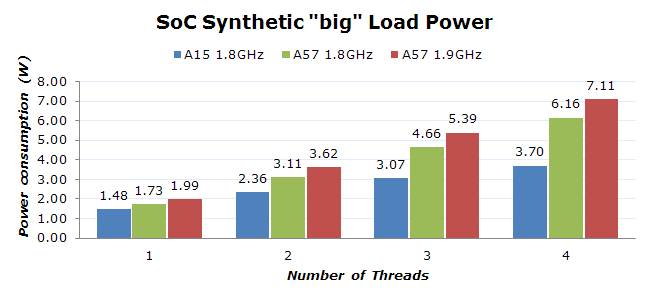
The difference in power is quite staggering. What jumps out immediately as out of the norm is the relatively low power consumption the 5430 is able to achieve. In the past we've seen A15 cores consume well north of 1.5W per core, something I've verified in the Exynos 5410 and Kirin 920. The combination of r3 A15 silicon IP and 20nm in the 5430 seems to have dramatically lowered the power consumption of the A15 to levels comparable to Qualcomm's Krait cores. It seems Samsung has gained a lot of experience with the A15 over the years and fed this back into the 5430, resulting in basically twice the power efficiency over past SoCs such as the 5420. But while the A15 numbers are interesting, we're here to check out the A57.
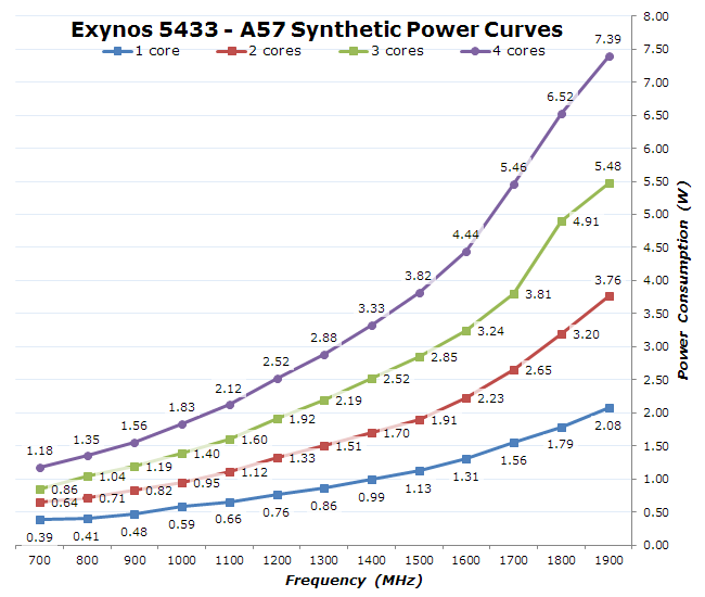
Alas, it doesn't look as good for the new cores. On a pure per-core basis it seems the A57 is about twice as power hungry. This is a significant figure that is quite worrisome. Investigating the voltages of the big cores on both SoCs reveals that the 5433 increases the voltage on the A57 cores by a rough 75mV across most used frequencies. We're averaging 1175mV at 1800MHz across the various speed bins, and reaching up to 1262mV on the worst speed bins at 1.9GHz. This results in some very high figures for the stock speeds of the 5433, being able to momentarily reach over 7W load on the big cluster. The thermal management doesn't allow this state to be sustained for more than 10 seconds when loading four threads, with the frequencies quickly dropping to the first thermal throttling levels.
I repeated my analysis over all frequency states and core count combinations, providing me with a detailed power curve for the A57 CPUs in the Exynos 5433:
I was able to catch the effect of temperature over power consumption in these tests: over the period of a minute power would continuously increase as the silicon heated up. After only 10 seconds of load the consumption would increase by 5%. Frequencies above 1600MHz especially suffer from this effect, as static power leakage seems to be increasing a whole lot on these states, so I wasn't able to account for the measured power to dynamic leakage alone. This might also be an effect of overhead elsewhere on the system; I imagine that the PMIC is working very hard at these kind of loads.
In any case, this points to the importance of having responsive and smart power management mechanisms that take into consideration not only frequency and voltage in their power modeling but also temperature. Luckily the Exynos 5433's power management is one of the best out there, having a full power arbitration system in place that does not allow the higher power figures for longer than short little bursts. Most work done should find itself in the lower frequencies, enabling much higher efficiency levels. The battery savings mode of the phone also caps the frequency of the A57 cores at 1400MHz, allowing for a very reasonable maximum 3.3W cap on the big cores while still providing excellent performance.
Again, we're able to get some rough estimates on the per-core power consumption figures for both SoCs running at equal frequency:
| Estimated Big Per-Core Power Consumption @ 1.8GHz | |||
| A15 (Exynos 5430) | A57 (Exynos 5433) | Increase | |
| Big per-core load | ~750mW | ~1480mW | 97% |
The A57 cores being an ARMv8 evolution of the A15 with only minor architectural additions beyond that shouldn't be that much bigger than the A15. Indeed we can see this in the block sizes of the SoCs:
| A15 vs A57 Block Sizes | ||||
| A15 (Exynos 5430) | A57 (Exynos 5433) | Scaling Factor | ||
| Core | 1.67mm² | 2.05mm² | 1.22 | |
| Cluster | 14.50mm² | 15.10mm² | 1.04 | |
We're seeing a much more conservative 1.22x scaling, less than the 1.75x found in the A53 cores. The total cluster size increases only by 4%, pointing out that Samsung made some improvements elsewhere on the cluster.
I repeat the XML test of BaseMark OS II to be able to give an impression of real-world performance/power.
| BaseMark OS II - XML Parsing Energy Efficiency | ||||
| Performance | Energy | Performance/Energy factor |
||
| A15 (Exynos 5430) | 99.69MB/s | 19.75mWh | ~5.04 | |
| A57 (Exynos 5433) | 155.29MB/s | 27.72mWh | ~5.60 | |
As opposed to the A53 which lost perf/W over the A7, the A57 actually gains efficiency over the A15. This shouldn't make sense given that the active power of the A57 seems to be roughly double that of the A15 on these specific SoCs. We go back to why I choose this particular test: the nature of the the XML test allows for cores to exercise their idle power states in a realistic manner.
ARM claims the A53 and A57 bring better and more fine-grained pipeline power- and clock-gating as part of the architectures, and my suspicion is that this is what we are seeing here in practice. I don't have other fitting devices at my disposal to be able to make an apples-to-apples comparison, but it seems that in daily real-world usages the A57 is able to outperform the A15 quite a bit in terms of power efficiency.
While we investigated both the A53 and A57 separately as individual clusters in the SoC, I was also very interested to see how the XML test would fare in the default big.LITTLE mode. We repeat the power measurement but leave the GTS parameters as configured by Samsung.
| BaseMark OS II - XML Parsing Energy Efficiency | ||||
| Performance | Energy | Performance/Energy factor |
||
| A7 (Exynos 5430) | 77.93MB/s | 10.56mWh | ~7.38 | |
| A15 (Exynos 5430) | 99.69MB/s | 19.75mWh | ~5.04 | |
| A7+A15 (Exynos 5430) | 76.53MB/s | 12.85mWh | ~5.95 | |
| A53 (Exynos 5433) | 109.36MB/s | 17.11mWh | ~6.39 | |
| A57 (Exynos 5433) | 155.29MB/s | 27.72mWh | ~5.60 | |
| A53+A57 (Exynos 5433) | 96.85MB/s | 18.77mWh | ~5.15 | |
What we're seeing here in our particular XML power efficiency test is that the whole mechanism falls flat on its face. For both the Exynos 5430 and Exynos 5433, the practical performance drops below what even the little cores would have been able to achieve on their own. While on the Exynos 5430 we lose efficiency over the little cores, it's still an improvement over letting the A15 cores handle the load alone. However when looking at the numbers of the 5433, things look bad. Running this benchmark on the default A53+A57 GTS mechanism not only is worse than simply running it on the little A53 cores, but it's also worse than letting the benchmark stay on the A57 cores. I could see the load jumping around between big and little cluster in a frequent manner.
As to why this performance degradation happens is not certain. I've been told that this may have been related to the way the benchmark was programmed and possible data-dependencies coming into play that cause an unusal overhead on the CCI. This is an interesting thought as this would be one particular case where ARM's newly announced CCI-500 interconnect would help out with the introduction of a snoop filter on the interconnect. I certainly did not aim for such a result in my search for a test-case micro-benchmark, but it raises the question of how many other real-world situations run into such bottlenecks.
It's also important to note that these numbers cannot be used as an argument against the efficiency of HMP itself. Running the big cores only is not a realistic use-case as there are vast power efficiency disadvantages in idle scenarios. A proper comparison would be if I had run the SoCs in a cluster-migration scheme and used that as a comparison point against the HMP operation. Sadly this is not a technically viable scenario for me to reproduce due to software limitations in the firmware. As such, these numbers are more of a representation of the A57 cores' efficiency rather than that of big.LITTLE and HMP as a whole.
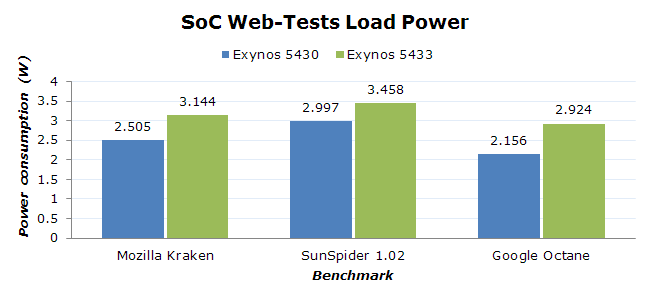
I've had some concerns raised to me for the fact that I don't have a fixed-load benchmark test in regards to power efficiency, so I went ahead and ran a power efficiency test on some of our web-browser tests. As a reminder, these tests may represent a real-world workload in terms of computations that are being done, but they don't represent a proper scaling load as we would find in real-world usage. For that, I have included some benchmarks in the battery section of the review which we'll investigate later in the article.
| Stock Browser - Web Tests Power Efficiency | ||||
| Score | Mean Power | Score/Power factor |
||
| Kraken (E5430) | 4973ms | 2.505W | ~80.27 | |
| SunSpider (E5430) | 449ms | 2.997W | ~743.13 | |
| Octane (E5430) | 5762 | 2.156W | ~2.67 | |
| Kraken (E5433) | 4160ms | 3.144W | ~76.45 | |
| SunSpider (E5433) | 395ms | 3.458W | ~732.11 | |
| Octane (E5433) | 7466 | 2.924W | ~2.55 | |
Before discussing the results I'd like to mention that I saw a huge discrepancy between Chrome and the stock browser. In Chrome, which I checked was indeed running the exactly same build version for both the Note 4 and the Alpha, I could see the Alpha consistently outperforming the Note 4 in all the tests. Due to this I deemed Chrome to be extremely unreliable as an apples-to-apples comparison of efficiency and reverted to the stock browser. Here I could see proper performance scaling that we would actually expect from the new core architectures and the clock advantage.
As for the browser efficiency scores themselves, what I see is that the Exynos 5430 again beats the 5433 in power efficiency, although this margin is just 4%. I have to reiterate again that we're dealing with Samsung's sixth generation of A15 SoC, and that's if we don't count consumer TV SoCs which also had A15 cores deployed over 2 years ago. The Exynos 5433 is only Samsung's second (after their unreleased GH7 server SoC) A57 implementation that we're seeing and it is also running at higher voltages on an immature process. I fully expect this gap to reverse in the future as we see vendors gain more experience with the IP and optimize their layouts and implementation.
I've talked in more detail on how currently HMP is implemented by vendors in the Huawei Honor 6 review which can be read here. For those who are still unfamiliar with the subject a quick explanation is that the current mechanism in the kernel that is used for controlling HMP operation is "GTS", or Global Task Scheduling. This mechanism is developed by Linaro, a consortium of ARM vendors which collaborate on the open-source software development side of SoCs. GTS is a Linux kernel modification that enables the scheduler to differentiate between the little and big cores of a system, and migrates tasks depending on their load.
The current mechanism as of late 2014 and found in all commercially available devices determines the decision of migrating a task on a target cluster with help of a geometric load value of a given task, a value that is defined by the kernel scheduler. The window in which the load is averaged depends on the vendor, but we've seen mostly 16ms in the case of Huawei and 32ms in Samsung's implementations. If a scheduler entity (a process) surpasses a certain upper threshold, the system migrates that entity to a fast cluster. Similarly, if it falls below a lower threshold, it is migrated to the slow cluster.
The problem with this approach is that the scheduler is totally unaware of the power consumption of the hardware when doing a migration. As a reminder, this process is done transparently in hardware via help of a cache-coherent bus interconnect such as ARM's CCI-400.
Not only does this cause migration overhead on the CCI due to cache flushes, but it messes with the idle mechanisms of the CPU. When a lower number of high load threads get migrated away from the big cluster and back to it, the cluster is allowed to enter its cluster power collapse state that also shuts down the L2 cache. This turning off and on of the cluster in repeated and high-frequency fashion consumes more power than had the load simply stayed on the big cluster and dealt with the active power penalty of the A57.
Samsung's implementation of GTS worsens this behavior as they employ a boosting mechanism that is tied with the interactive CPU frequency governor and user-space triggers such as switching applications or touchscreen events via the touch-booster mechanism. The boost here temporarily lowers the migrations thresholds to very low levels (15% down, 40% up) to be able to improve device fluidity.
In my opinion this is overkill as trivial tasks such as scrolling through an application like Reddit Sync (with already loaded content) causes the processes to reside on the big cluster. It's possible to disable this behavior via the power savings mode of the device. In my example of the Reddit app there is no discernable loss of fluidity when just scrolling through posts, and the big cores remain idle, making for much lower power consumption. The disadvantage of the power savings mode is that it caps the CPU to 1.4GHz and the GPU to 350MHz. I wish Samsung would provide a two-stage power savings mode where we could control both the boost mechanic and the clock frequency limits separately.
It's been over two years since the first big.LITTLE SoCs were introduced, and even if we ignore the first generations such as the Exynos 5410 and 5420 that were limited to cluster-migration schemes, ARM has had plenty of time to produce a more effective software stack that takes advantage of big.LITTLE. The fact that the Note 4 is using a 14-month old implementation of GTS that is lacking some key improvements in the scheduler in terms of power management demonstrates a grave problem of the big.LITTLE approach, as the software represents the Achilles' Heel of the technology and severely limits its potential.
ARM and Linaro are working on a solution for upstream Linux that has been discussed for well over a year. To this day the power-aware scheduler still hasn't seen a definitive implementation, and when we brought up the issue with ARM they admitted that progress has been slow due to the fundamental changes the solution requires and the many stakeholders it involves. The process has been complicated by the fact that ARM wants to get it right the first time and work in a generic solution that can be carried over to future ARM SoCs, a process that takes longer than implementing a one-off non-upstream solution for a specific product.
Meanwhile ARM is also calling attention to their Intelligent Power Allocation project for upstream Linux. Like the new power-aware scheduling solution, it too has yet to make it upstream. IPA has already seen limited adoption in shipping products in at least Samsung's devices, and ARM believes it can mitigate some of the issues related to the scheduler. While IPA is an excellent thermal management implementation, it cannot serve as a replacement for a proper mechanism that tries to optimize power efficiency in HMP operation, as it has no control over where a task is placed on the CPUs. Also, IPA is only enabled when the SoC passes a certain threshold temperature and any arbitration below that is still left to the kernel scheduler.
In any case, I'd wager we won't be seeing ARM's power aware scheduling solution in devices for well over another 18 months at minimum. Meanwhile, Qualcomm is entering the big.LITTLE ring with its own Snapdragon 810 with a fully working, custom-developed, and power-aware scheduler implementation that alleviates many of the issues I've identified here in this piece.
In the future, I hope Samsung SLSI invests more time and R&D in its software implementations, as being first to market with the hardware and relying on Linaro's basic software stack simply isn't enough if they wish to continue using big.LITTLE as the corner-stone of their SoCs.
Mali T760 - Architecture
The Midgard GPU architecture has been around for over two years now since we saw the first Mali T604MP4 implemented in the Exynos 5250. Since then ARM has steadily done iterative improvements to the GPU IP resulting in what we now find in the Exynos 5433: the Mali T760. Over the last summer we've had the pleasure of getting an architectural briefing and disclosure from ARM, which Ryan has covered in his excellent piece: ARM’s Mali Midgard Architecture Explored. It's a must-read if you're interested in the deeper workings of the current generation Mali GPUs employed by Samsung and other vendors.
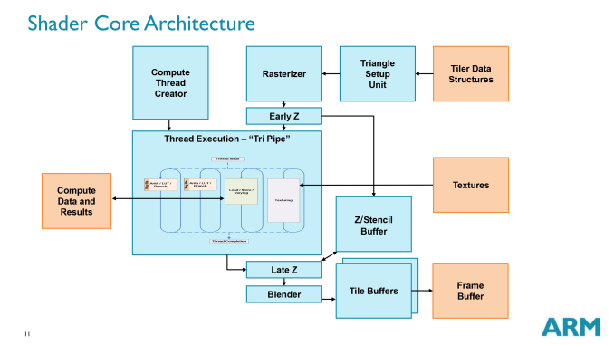
The T760's predecessor, the T628, has been now used for over a year in the Exynos 5420, 5422, 5430, 5260 and HiSilicon Hi3630, and regrettably it wasn't as competitive as we would have wished, in terms of performance and in power efficiency. Hoping that the T760 brings the Mali GPU in better competitive shape, there are two main points that we should be expecting from the T760 in terms of advancements over the T628.
- Improved power efficiency due to internal wiring optimizations between the cores and the L2 cache.
- Improved performance and power efficiency due to both reduced bandwidth usage and increases in effective usable bandwidth by help of ARM Frame-Buffer Compression (AFBC).
Mali T760 - Synthetic Performance
To be able to do an architectural comparison, I lock the T628 and T760 to 550MHz so that we can get a directly comparable perf/MHz figure for both architectures. Since both SoCs have the same internal bus architecture, same memory speed, and even same cache sizes on the GPU, performance differences should be solely defined by efficiency gains of the new architectural additions of the new Midgard GPU in the Exynos 5433. To do this we use GFXBench as the base comparison benchmark as it is our de-facto benchmark for graphics.
| GFXBench @ 550MHz Offscreen | ||||||
| Mali T628MP6 | Mali T760MP6 | % Advantage | ||||
| Manhattan | 12.8 fps | 14.5 fps | 13.2% | |||
| T-Rex | 31.5 fps | 35.1 fps | 11.1% | |||
| ALU performance | 42.4 fps | 41.6 fps | -1.8% | |||
| Alpha-blending | 3006.5 MB/s | 3819 MB/s | 27% | |||
| Driver overhead | 29.1 fps | 45.05 fps | 55.3% | |||
| Fill-rate | 2907 MTexels/s | 3120 MTexels/s | 7.3% | |||
If we begin with the synthetic numbers first, we see that there is a non-change in ALU throughput, with only a minor 1.8% decrease in performance over the T628MP6. The tri-pipe design hasn't changed on the T760 so this was an expected result. The small decrease could be attributed to many things but I don't think it's worth any serious attention.
It's on the alpha-blending test things get interesting: performance jumps 27% compared to the T628 at the same frequency. I initially thought this would have been an effect of AFBC and the resulting increased bandwidth, but ARM has explained this is an architectural improvement of the new Midgard generation on the T7XX series. The 7.3% fill-rate increase might also be a gain of this particular addition to the T760.
Completely unrelated to any architectural changes is a massive 55% boost in the driver overhead score. The Galaxy Alpha shipped with an r4p0 driver release while the Note 4 sports r5p0 Mali drivers. This is an outstanding increase for Android as it not only gives the T760 and ARM's new drivers a big advantage over its predecessors, but it also now suddenly leads all Android devices in that particular benchmark by a comfortable margin.
We've seen that Android devices have traditionally suffered in this test while iOS phones and tablets lead by a factor of 3x. This confirms a long-standing suspicion that we're still a long way from achieving acceptable driver overhead on the platform. I was curious as to what ARM did here to achieve such a big increase, so I reached out to them and they happily responded. The r5pX drivers improve on three main areas:
- Workload efficiency: The shader compiler was updated to make better use of the shader pipelines and achieve better cycle efficiency; in the case of the T760 there are also optimizations to AFBC usage.
- Improved driver job scheduling: Improvements to the kernel job scheduler making sure that hardware utilization is as close to 100% as possible.
- Overall optimizations to reduce CPU load, allowing for more performance in CPU-bound scenarios and otherwise lower power consumption.
At the same time it should be noted that CPU performance certainly also plays a part in driver overhead scores - when measuring overhead we're essentially measuring how much CPU time is being spent on the drivers - though how big of a role is up for debate. A57 in particular offers some solid performance increases over our A15-backed Exynos 5430, which can influence this score. However in testing, by lowering the CPU performance I was only able to get down to 29fps in the driver overhead test when limiting the frequency to 1 GHz on the A57 cores, giving much lower performance than the what the 1.8GHz A15 would achieve.
Based on the above, I believe that if ARM can bring these driver improvements to previous generation devices there should be a sizable performance boost to be had. It won't be as great due to the lack of the corresponding A57 CPU, but it should still be a solid boost.
Overall, the aggregate of these new technologies can be measured in the Manhattan and T-Rex practical tests. Here we see an 11-13% increase of performance per clock. Ultimately this means that the raw performance gains from the T760 alone are not going to be huge, but then as T760 is an optimization pass on Midgard rather than a massive overhaul, there aren't any fundamental changes in the design to drive a greater performance improvement. What we do get then from T760 is a mix of performance and rendering efficiency increases, power efficiency increases, and the possibility to be a bit more liberal on the clock speeds.
Power Consumption
I was first interested to see how ARM's GPU would scale in power and performance depending on core count. To do this I locked the system again to the little cores as to avoid any power overhead the A57 cores might have on the measurement. I locked the GPU to 500MHz as I wanted to do a direct comparison in terms of scaling with the T628 and chose that frequency to run both devices; however, that ended up with bogus numbers for the T628 as there seems to be some misbehavior in the drivers of the Galaxy Alpha when trying to limit the core count to less than the full 6-core configuration.
In any case, I was more looking to get an impression of the inevitable overhead of the CPU and rest-of-SoC and how power consumption scales between cores. I'm using GFXBench's T-Rex Offscreen test to measure these power figures, again with already-accounted screen and system idle power consumption.
As we see in the chart, using additional cores on the Mali T760 seems to scale quite linearly. Adding an additional core adds on average another 550mW at 500MHz to the total power consumption of the system. If we actually go subtract this figure from the MP1 power value we end up with a difference of around 550mW that should be part CPU, RoS (Rest-of-SoC), memory, and common blocks on the GPU that are not the shader cores. Of course this is all assuming there is no power increase on the CPU and RoS due to increased load of the GPU. It's quite hard to accurately attribute this number without doing hardware modifications to the PCB board to add sense resistors to at least five voltage rails of the PMIC, but for our purposes it gives a good enough estimate for the now following measurements.
As mentioned I wanted to include the T628 in the same graphs, but due to driver issues I can only give the full-core power consumption numbers. The Exynos 5430 used 3.74W at the same 500MHz lock; this 110mW difference could very well be just the increased consumption of the A53 cores over the A7 cores, so it seems both GPUs consume the same amount of power at a given frequency.
In terms of performance, the Mali T760 scaled in a similar way as the power consumption:
| Mali T760 Core Performance Scaling @ 500MHz | ||||||
| MP1 | MP2 | MP3 | MP4 | MP5 | MP6 | |
| fps | 5.8 | 11.5 | 17 | 22.5 | 27.6 | 32.2 |
| fps per core | 5.8 | 5.75 | 5.66 | 5.62 | 5.52 | 5.36 |
We see a slight degradation of ~1-1.5% on the per-core fps with each additional core but this seems within reasonable overhead of the drivers and hardware. All in all, the scaling on Mali T760 seems to be excellent and we should be seeing predictable numbers from future SoCs that employ more shader cores. The T760 supports up to an MP16 configuration, and while I don't expect vendors to implement this biggest setup any time in the near future, we should definitely see higher core numbers in future SoCs this year.
Again, I can only give the MP6 number for the T628 here: 26.2fps. This means that the T760 is roughly 23% more efficient in terms of perf/W than its predecessor while operating at the same frequency. In the aspect of silicon efficiency, this is also an improvement. The Mali T760MP6 on the 5433 comes in at 30.90mm² 25mm² of the total SoC area, only a meager 0.29mm² more than the T628MP6 in the Exynos 5430.
While until now I was measuring performance and power consumption at a fixed frequency for facultative reasons, it's time to see what the GPU is actually capable of at it's full frequency. But there's a catch.
While I initially reported that the T760 on the 5433 was running at 700MHz, and that frequency is indeed used as a maximum of the DVFS mechanism, there's also a secondary maximum frequency of 600MHz. How can this be? In fact the DVFS mechanisms of both the 5430 and 5433 have a new addition in their logic that is both very unusual and maybe, dare I say, innovative in the mobile space.
Until now, and for all other SoCs other than these two, classical DVFS systems would base their scaling decision on the general load metric provided by the GPU drivers. This is normally computed by reading out some hardware performance counters from the hardware. The DVFS logic would take this load metric and apply simple up- and down-thresholds of certain percentages to either increase or decrease the frequency.
In the case of both 5430 and 5433, Samsung goes deeper into the architecture of the Mali GPU and retrieves individual performance counters of each element of a tri-pipe.

It evaluates the individual load of the (combined) arithmetic pipelines (ALUs), load/stores unit (LS), and the texture (TEX) unit. What it does is that when the load on the LS unit exceeds a certain threshold, the higher DVFS frequency of 700MHz is blocked off from being reached. Similarly it also denies the higher frequency when the ALU utilization is greater than 70% of the LS utilization.
In practice, what this does is that workloads that are more ALU heavy are allowed to reach the full 700MHz while anything that has a more balanced or texture-heavy usage stays at 600MHz. This decision making is only valid for the last frequency jump in the DVFS table, as anything below that uses the classical utilization metric supplied by the ARM drivers. This is the main reason why I needed to cap the GPU frequency to a P-state that is not affected by this mechanism, as it's not possible to disable it by traditional means and I needed to run the same frequency on both the T628 and T760 for the synthetic performance benchmarks.
Now as to why this matters for the general user, the 700MHz state in the Exynos 5433 comes with a vastly increased power requirement, as it's clearly running a high overdrive state at 1075mV versus 975mV at 600MHz. This means that the 700MHz state is 42% more power hungry than the 600MHz state, and in fact, we'll see this in the full power figures when running under the default DVFS configurations.
On the T628 this overdrive state happens on the 550MHz to 600MHz frequency jump. Here the power penalty should be less heavy as the voltage and frequency jump account for a "mere" theoretical 13% increase.
I've always suspected that the Manhattan test was more of an ALU heavy test compared to past Kishonti benchmarks. What this peculiar DVFS mechanism on the 5433 allowed me to do is actually confirm this as I could see exactly what is happening on the pipelines of the GPU. While the texture load is more or less the same on both Manhattan and T-Rex, the load/store unit utilization is practically double on the T-Rex test. On the other hand, Manhattan is up to 55% more ALU heavy depending on the scene of the benchmark.
The result is that power draw in Manhattan on the 5433 is coming in at a whopping 6.07W, far ahead of the 5.35W that is consumed in the T-Rex test. Manhattan should actually be the less power hungry test on this architecture if the tests were to be run at the same frequency and voltages. We can see this in the Exynos 5430, as the power draw on Manhattan is lower than on T-Rex, even though it's using that 13% more power intensive 600MHz hardware state.
Why Samsung chose to bother to implement this state is a mystery to me. My initial theory was that it would allow more ALU heavy loads to gain performance while still keeping the same power budget. ARM depicts the ALU inside the tri-pipe diagram in a smaller footprint as the LS or TEX units, which traditionally pointed out to a very rough correlation of the actual size of the blocks in silicon. The huge jump in power however does not make this seem viable in any realistic circumstance and definitely not worth the performance boost. I can only assume Samsung was forced to do this to close the gap between the Mali T760 and Qualcomm's Adreno 420 in the Snapdragon 805 variant of the Note 4.
I have yet to do a full analysis of today's current games to see how many of them actually have a heavy enough ALU workload to trigger this behavior, but I expect it wouldn't be that many. BaseMark X for example is just on this threshold as half the scenes run in the overdrive state while the other half aren't ALU heavy enough. For everything else the 600MHz state is the true frequency where the device will cap out.
| Exynos 5430 vs Exynos 5433 T-Rex Offscreen Power Efficiency |
||||||
| FPS | Energy | Avg. Power | Perf/W | |||
| Exynos 5430 (stock) | 31.3 | 80.7mWh | 5.19W | 6.03fps/W | ||
| Exynos 5433 (stock) | 37.7 | 91.0mWh | 5.85W | 6.44fps/W | ||
| Exynos 5430 (little lock) | 29.3 | 73.2mWh | 4.71W | 6.23fps/W | ||
| Exynos 5433 (little lock) | 37.3 | 88.6mWh | 5.70W | 6.55fps/W | ||
The end power/W advantage for the T760 at its shipped frequencies falls down to under 6% because of the higher clocks and voltages. Another peculiarity I encountered while doing my measurements was that the Exynos 5430 was affected much more by limiting the system to the little cores. Here the Mali hits CPU-bound scenarios immediately as the scores drop by 7% on the off-screen test and a staggering 26% on the on-screen results of T-Rex. Usually GFXBench is a relatively CPU light benchmark that doesn't require that much computational power, but the A7 cores are still not able to cope with simple 3D driver overhead. The 5433 on the other hand is basically not affected by this. This is a very good improvement as it means much less big core activity while gaming, one of big.LITTLE's most damning weak-points.
I'm still not satisfied with the power consumption on these phones, a little over 5.7W TDP is certainly unsustainable in a phone factor and will inevitably lead to thermal throttling (as we'll see in the battery rundown). Apple's SoCs here definitely have a power efficiency advantage no matter how you look at it. I'm curious to see how an Imagination GPU would fare under the same test conditions.
All in all, as the T700 series is largely an optimization pass on Midgard, the resulting T760 brings some improvements over its T628 counterpart but it's not as much of an improvement as I'd like to see. Since doing these measurements I've received a Meizu MX4Pro that also sports an Exynos 5430, but it came with an average binned chip as opposed to the almost worst-case found in the Galaxy Alpha that I've used for comparison here. In preliminary measurements I've seen almost a 1W reduction in power over the Alpha.
This leaves me with a blurred conclusion on the T760. There is definitely an improvement, but I'm left asking myself just how much of this is due to the newer drivers on the Note 4 or just discrepancies between chip bins.
CPU and System Performance
While we've gone over some hefty material till now, we're still missing a crucial comparison for the Note 4 with Exynos 5433. How does it fare against the Snapdragon 805 version?
For this comparison we go to check one last time the estimated SPECint2000 score of the two devices. Again, this benchmark is purely for an architectural comparison between Qualcomm's Krait cores and ARM's new A57 CPUs. This is an outdated and deprecated benchmark and isn't really representative of mobile workloads, but it gives a good idea of synthetic CPU performance.
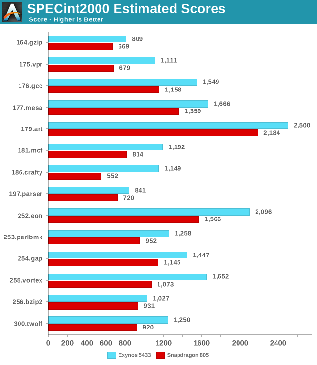
Qualcomm's Krait core is by now almost three years old - a long time since we first saw the first Snapdragon S4 phones come out. Qualcomm has been able to squeeze a lot of life out of the architecture with the help of incremental updates, but now it's clearly reaching its limits. At 2.7GHz the device is still at an estimated 37% overall disadvantage against the 1.9GHz clocked A57 in the Exynos 5433 variant.
The Snapdragon 810 is just around the corner and we'll be seeing Qualcomm adopt ARM's new ARMv8 cores instead of relying on their own design. Qualcomm is certainly working on their own custom ARMv8 core, but there's still not much in the way of details other than to expect it around roughly a year from now. As it stands, the first half of 2015 seems to be dominated by A57 SoCs.
We continue on to our more classic set of browser JavaScript based benchmarks. This time around I'm including the stock browser scores alongside Chrome to demonstrate an issue I'll be getting to in just a bit...
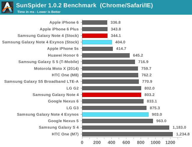
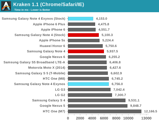
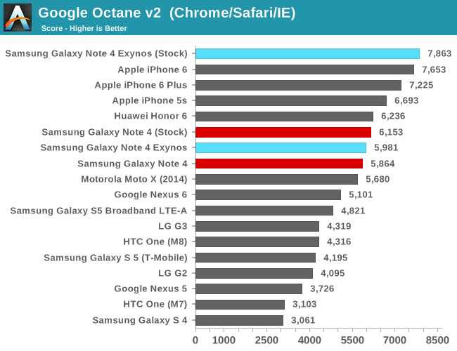
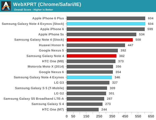
What we're seeing here is an increasing problem of our browser benchmarks. Vendors have optimized their stock browser libraries to target the specific CPU and GPU of a given device to be able to squeeze all possible performance out of the hardware. This aspect grows increasingly important as the architectures start to vary quite a lot between each other. Here employing Chrome as-is by Google is a great disadvantage as it's not optimized for any one platform. Google offers partial solutions (e.g. the Chrome Samsung Support Library which enables Chrome to use some stock OS browser libraries - a definite improvement in speed over vanilla Chrome), but it hasn't seen an update in over eight months and doesn't work on the Exynos 5433.
With significant performance improvements of the ARMv8 cores of the Exynos 5433 needing at least an AArch32 compiled code-base for them to be unleashed, it's natural to try to stick to Samsung's own solutions until the Android ecosystem gets updated. Curiously, the Snapdragon 805 also benefits from the stock browser, meaning Samsung is also extensively optimizing for that platform.
The scores on the Exynos version of the Note 4 are outstanding, beating out all existing devices in our more complex benchmarks. SunSpider is the exception, but seeing the vast discrepancy between browsers and even the Snapdragon version matching Apple's new A8 has made us come to the conclusion that this benchmark has run it's time as a valid test case, and thus we're dropping it from our 2015 test suite going forward.
Heading over to BaseMark OS II as our more general system benchmark, we see again the Exynos version outperform the Snapdragon. It's not quite enough to beat Apple's A8 processor in the new iPhones, still lagging a bit behind their custom architecture and OS.
We'd like to mention that there has been a big overhaul in BaseMark OS II in a recent December release, fixing various issues regarding score computation, and it also introduced changes in the benchmarks themselves. As such, the new scores are not directly comparable to reviews published in the past. We've re-run the most recent flagship devices through the new benchmark and will go forward with the new version for future articles. The new scores are now labeled "BaseMark OS II 2.0" instead of "BaseMark OS II".
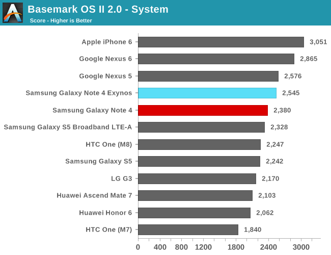
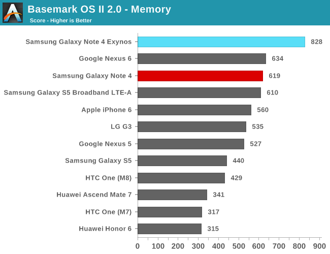
The memory test is a general NAND speed test. Here the Exynos version is outperforming the Snapdragon by quite a bit. This is intriguing as one would expect both versions to employ the same eMMC, but that's not the case. This Exynos version uses an R21AMA eMMC chip while our tested Snapdragon unit has an R218MA chip. They're both 32GB units, so I'm not too sure if there's a performance delta between what appears to be different series of this eMMC model or if this can be attributed to Samsung's use of a more performant Synopsys DesignWare MMC controller in the Exynos compared to Qualcomm's own SDCC. I double checked this in our AndroBench test and there there was no significant deviation from the Snapdragon review unit, so this might just be a peculiarity of the specific load of the memory test in BaseMark OS II that favors the Exynos eMMC controller and SoC architecture.
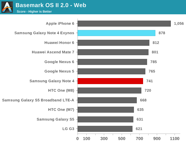
The web test is dependent on resolution as it's rendering an HTML canvas elements and doing CSS transformations on-screen. The Exynos Note 4 leads all other Android devices, only again coming short of the iPhone 6 - but one must keep in mind this test is resolution dependent and the iPhone's lower resolution for sure helps.
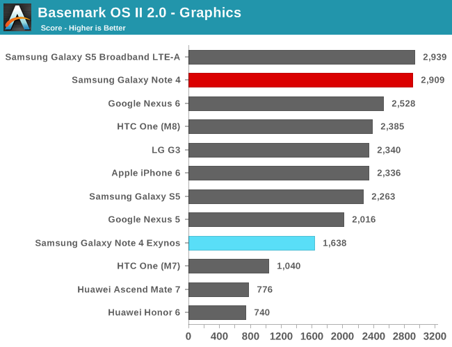
The graphics test again is dominated by the Snapdragon version of the Note 4. The Adreno 420's vast ALU and fillrate throughput are clearly visible as it manages to separate itself from the competition. The Mali T760, while still leading the ARM pack, is well behind Qualcomm's and Imagination's GPUs.
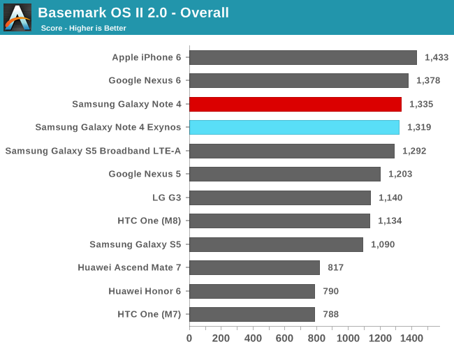
Due to the underwhelming graphics score, it brings down the overall result of BaseMark OS a bit beneath that of the Snapdragon version of the Note 4.
As part of our 2015 test suite we're introducing Futuremark's PCMark for Android into our mobile device reviews. PCMark is an overall system workload that uses Android's built-in libraries and APIs, a very common use-case that we find in a lot of Android applications.
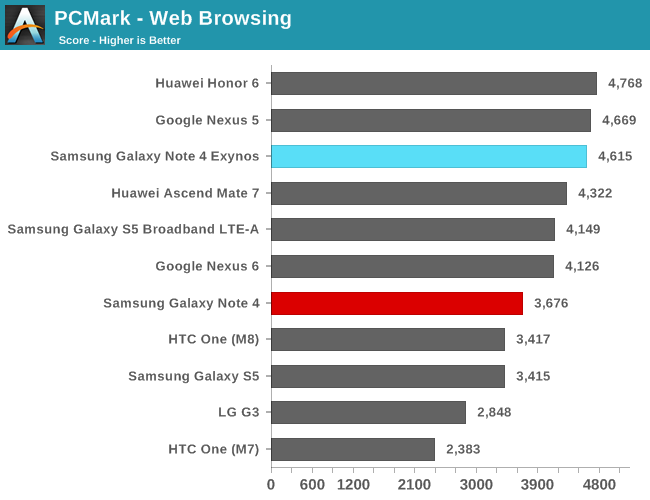
The web browsing test on PCMark uses a native Android WebView to display and interact with the web pages. It tests performance by measuring time to render pages, search for content (JavaScript performance), and time to re-render the page as images are altered.
Here we see the Exynos version again outperforming the Qualcomm Note 4 by a substantial amount. It's also interesting to see the Nexus 5 and Honor 6 that high up on the test, definitely a sign of how this is a system test rather than just a purely synthetic CPU performance test.
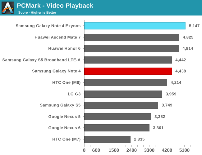
The video playback test uses the native Android MediaPlayer API to play back a 1080p H.264 baseline 4.0 video, with a variable target bit rate of 4.5Mbps at 30 FPS. What is measured here is the time needed to open the video samples, their average frame rates, and the seek time when skipping through the videos.
The Exynos is again at the top, outperforming all other benchmarked devices. Beyond testing the OS and API performance, this is also a test stressing the hardware as it tests the eMMC speed and the hardware decoder of the devices. We're seeing top notch performance from Samsung's device here as the video loads and seeks virtually instantly. I've seen excellent performance from Exynos hardware decoders ever since the Galaxy S2 and the Exynos 4210, which back in the day (as opposed to the competition) had no issues with even heavy 50Mbps streams. It seems Samsung is continuing that trend to this day.
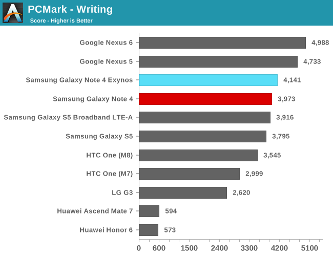
The writing test measures performance when manipulating a native EditText view. It loads, decompresses, and pastes two documents together into a large 200k character piece of text. This is then compressed into a ZIP and saved. Further text manipulation is done and the API overhead and performance is measured.
The Exynos has a slight edge over the Qualcomm Note 4, but they're both beat out by the Android 5.0 Lollipop Nexus 5 and 6 devices. I'm happy to see a test being able to measure general UI and API performance on Android as it's an aspect of device performance that was rarely touched upon.
As a side note, I've seen abysmal performance on my Huawei devices for this test. It seems there is some issue in EmotionUI that leads the Mate 7 and Honor 6 to lag behind by a considerable amount in this benchmark.
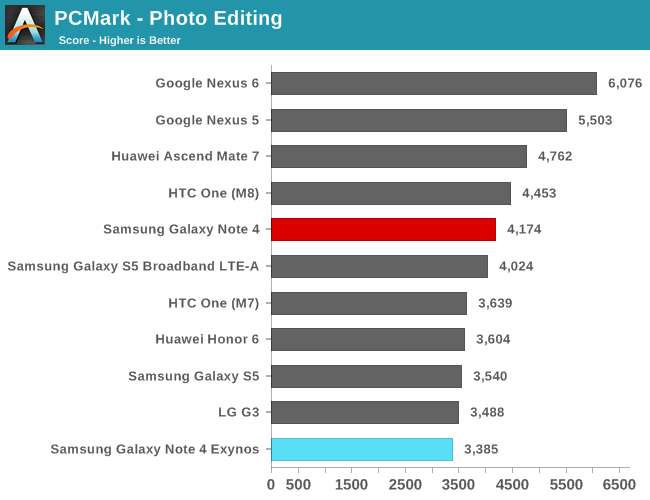
The photo editing test is a mix between API performance and both GPU and CPU performance. Image effects are applied via both the native effect API in Android as well as a RenderScript that tests heterogeneous processor performance (GPU and CPU). Additionally a Java library is used to test Java performance through processing filters that are computed on the CPU.
We see the Exynos performing last in this test-case, while our Lollipop devices lead the pack. It seems this is an issue with the OS libraries as the Mate 7, which also employs a Mali GPU, performs quite well in this test, pointing out that it's not a hardware performance limitation.
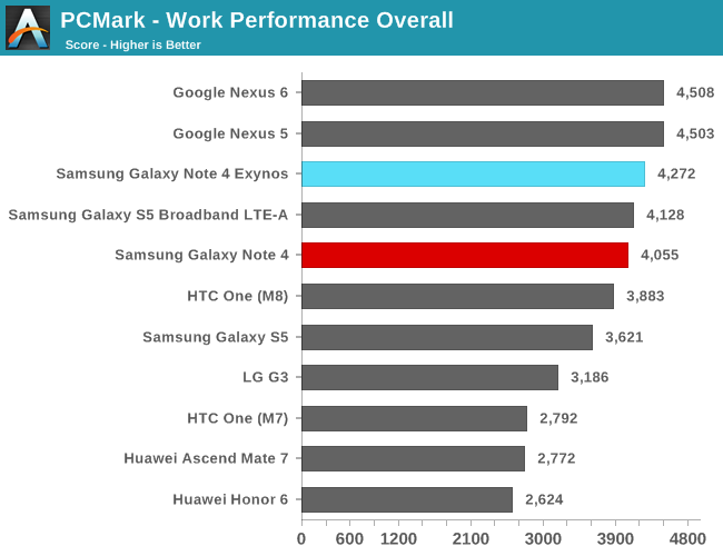
The overall work performance score for the Exynos Note 4 falls slightly ahead of the Qualcomm version. It will be interesting to see how the battlefield changes as more devices get updated to Lollipop; there's evidently a large performance boost to be expected as portrayed by our Nexus 5/6 numbers.
Overall, the Exynos's CPU is much ahead of the Snapdragon. This is not only seen in benchmarks but also real-world usage as the device is snappier and more fluid. Some people might notice microstutters on the Snapdragon version; Qualcomm is still relying on CPU hot-plugging for their power management. Hot-plugging is a Linux kernel operation that takes a CPU out of coherency and is a slow and expensive operation that forces the device to stop for a certain time. This overhead has been vastly reduced over the years as things were optimized in the Linux kernel, but it is still very much an unfavorable mechanic nowadays. Modern ARM Cortex CPUs now use their power collapse states via the CPUIdle framework, which avoids such issues.
Next let's inspect the graphics performance of the Exynos Note 4.
GPU Performance
In the graphics department we're matching up Qualcomm's Adreno 420 versus the Mali T760MP6. The Adreno is running at 600MHz and is able to benefit from almost double the memory bandwidth at 25.6GB/s versus 13.2GB/s due to the Snapdragon's increased 128-bit memory interface. Let's look at how both compare in our overall benchmarks:
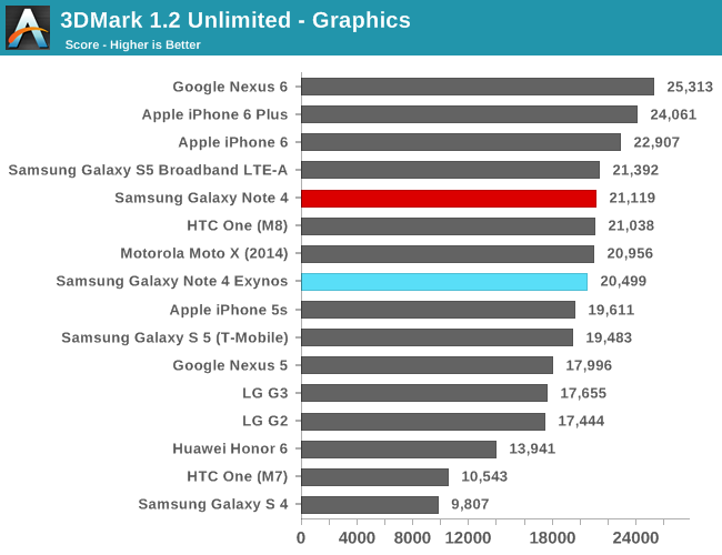
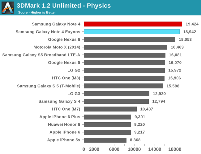
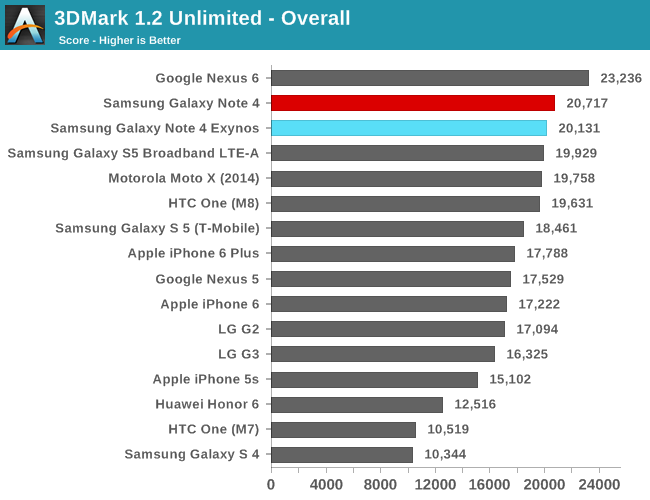
In 3DMark Unlimited the Exynos version comes just short of a few fps behind the Adreno 420. What is also surprising is that the Exynos 5433 performs much better in the physics score than I had anticipated; the same test on Huawei's SoCs limited the thread onto the little cores in the default settings giving mediocre performance results. However, it seems the A53 is performing much better and is able to match Qualcomm's offering now.
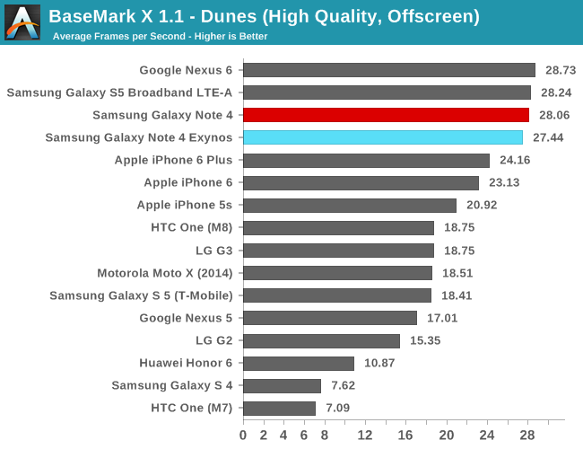
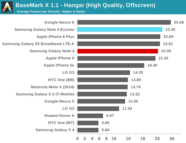
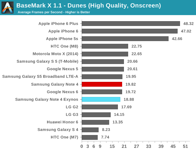
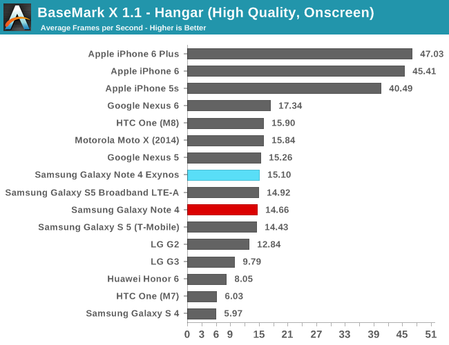
In BaseMark X 1.1, the Exynos is again neck-and-neck with the Snapdragon version. It loses by a slight margin in the Dunes benchmark while winning in the Hangar scenes by a similarly small margin. BaseMark X is again one of the benchmarks that can trigger the 700MHz state of the Mali GPU, offering higher performance at a much higher power draw depending on which scene is currently rendered on both tests.
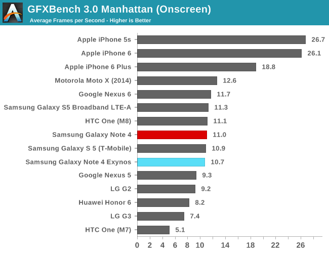
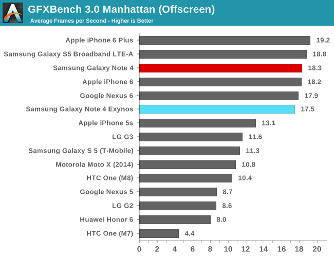
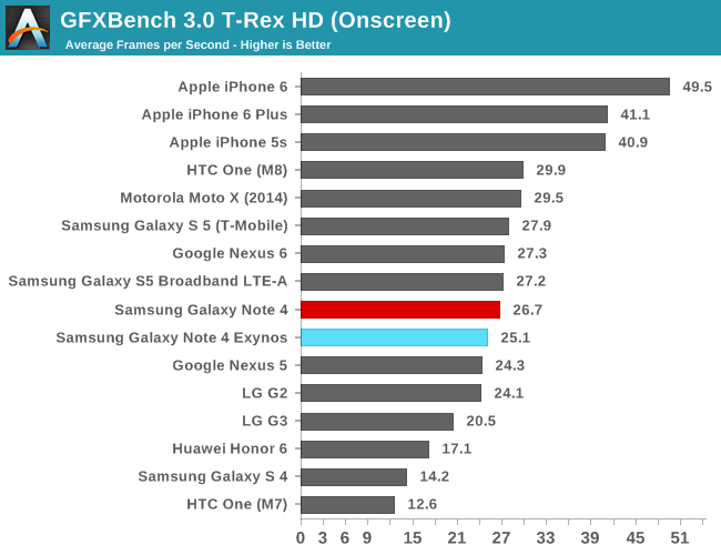
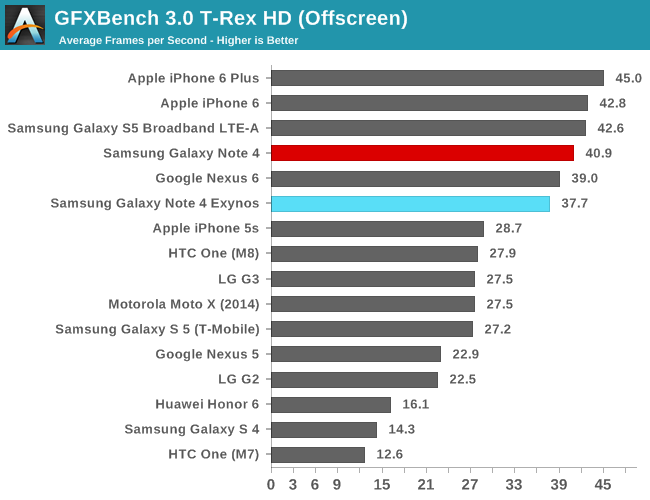
Again we continue to see the same pattern in GFXBench's scenario benchmarks, with the Exynos version lagging a few frames behind the Qualcomm GPU in both Manhattan and T-Rex, in both on-screen and off-screen results.
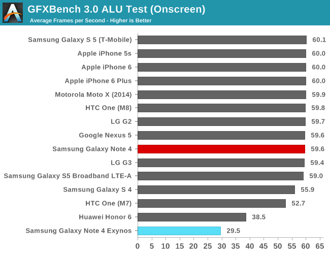
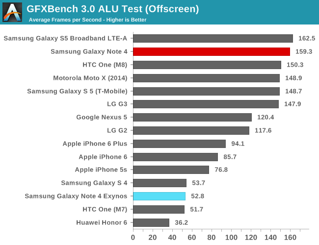
It's on the synthetic tests that we finally see some major deviation between the two architectures. ARM's Mali simply can't seem to keep up with the ALU throughput of Qualcomm's architecture. Both the Adreno 330 and 420 have a clear computational power advantage, exceeding even Imagination's PowerVR GPUs in the iPhones, leaving Mali strictly on the lower end of the performance spectrum.
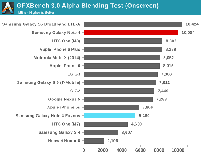
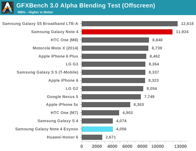
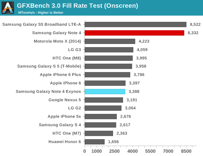
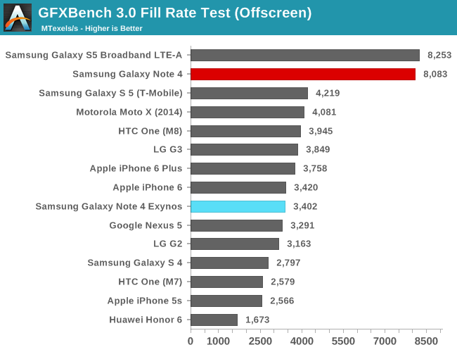
We see a similar situation in the Alpha Blending and Fillrate tests, as the Adreno offers 2-3x the throughput. Utilizing the extra memory bandwidth here seems to be key to the success of the Snapdragon 805's graphics performance.
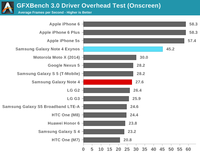
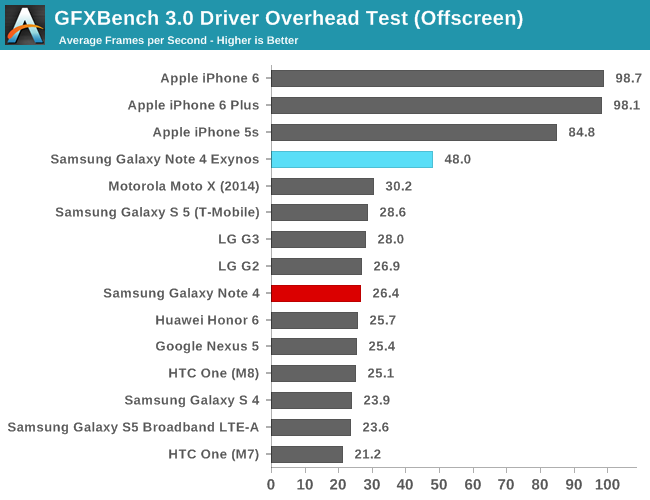
I've already mentioned the Driver Overhead score in the the more in-depth analysis of the T760. It's the first Android device to truly stand out from the rest of the crowd, finally making some progress into trying to catch up with Apple's excellent performance on iOS. Here's hoping more vendors concentrate on improving this metric in future driver updates.
I did some extensive power measurements on the Note 4 Exynos in this review, so naturally we're keen to see how this transforms into our battery benchmarks on the next page.
Battery Life
Both the Note 4 Exynos and the Snapdragon version sport the same size 3220mAh 3.85V battery. The difference is in the internal components, one running off Qualcomm's Snapdragon 805 platform that includes their own PMIC, audio solution, and modem IC. On the other hand Samsung provides their own PMIC too, but relies on audio solutions from WolfsonMicro and modem from Ericsson.
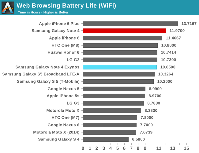
Unfortunately the battery disadvantage for the Exynos versions is quite large in our web browser benchmark. Here the Exynos comes out 79 minutes shorter than the Qualcomm version. I commented in the A57 page how bad Samsung's software power management is on the Exynos 5430 and 5433, running a quite outdated version of GTS to control big.LITTLE migration in the Linux kernel scheduler. I see this result as a direct consequence of an inferior configuration in terms of CPUIdle drivers and lacking big.LITTLE optimization. I mentioned in the A53 power analysis that the kernel is lacking several power management features such as "Small Task Packing".
In the time between starting this article and publishing it, I was able to confirm this and improve the power efficiency by applying a handful of patches onto the stock kernel. I'm looking forward and hoping to do a more in-depth article about user-customization of device firmware in the future, especially on the topics of overclocking and undervolting in the mobile space.
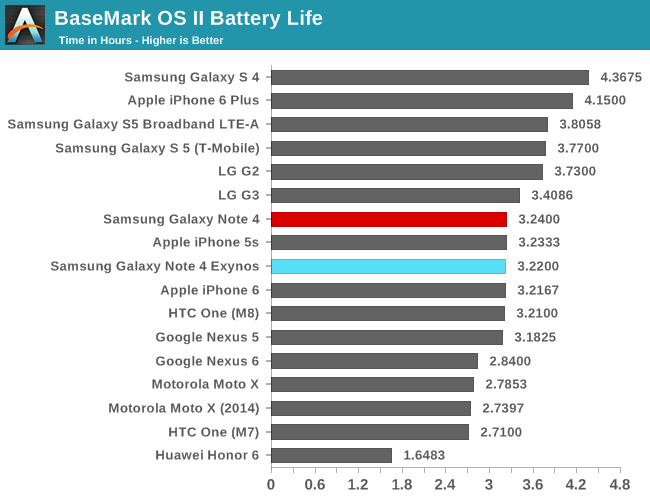
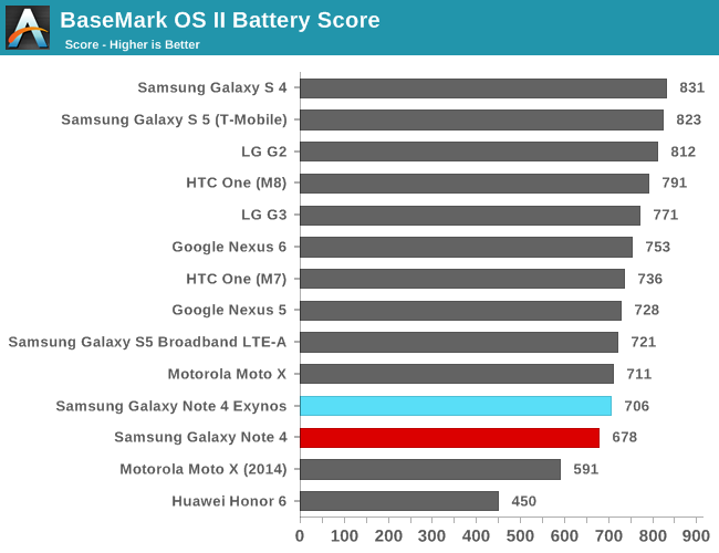
The BaseMark OS II Battery benchmark is a CPU run-down test. Here we're seeing the devices limited by thermal drivers and power allocation mechanisms. Both the Exynos and the Qualcomm are neck-and-neck in this benchmark, representing around 3.85W total device TDP. The Exynos is able to do more work in the same period, awarding it a slightly higher battery score.
Since we are adding PCMark to our 2015 suite, I decided it would also make a good test candidate for overall device power consumption. For this I measure the power draws during the various subtests. These figures portray total device power, meaning the screen is included in the measured power. The video test in particular is something that will be interesting as we have stopped publishing video playback battery life because modern devices routinely exceed 12 hours of lifetime.
Although we can't do much with the device power figures without having comparison devices, we can see the power differences between running the device in normal versus power-savings mode. The power savings mode limits the A57 cluster to 1.4GHz and disables all boost logic in the scheduler, meaning the threads are no longer aggressively scheduled on the big cluster due to lowered migration thresholds.
It's interesting to see the perf/W go up in battery savings mode. I've commented in the A57 section how Samsung's default scheduler settings are much too aggressive in normal usage and may have detrimental effects on power consumption. The figures presented by PCMark corroborate my suspicions as real-world loads are negatively impacted in power efficiency.
I hope to continue using PCMark as a power consumption test in future devices whenever it's possible so that we can paint a better picture of general power consumption of devices.
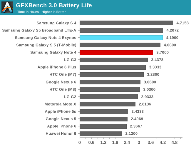
On the GFXBench battery rundown the Exynos leads the Snapdragon by half an hour. It's worth mentioning that I ran this several times while Josh ran his review unit under different ambient temperature conditions; we found the score can fluctuate a lot depending on much heat the phone is allowed to dissipate.
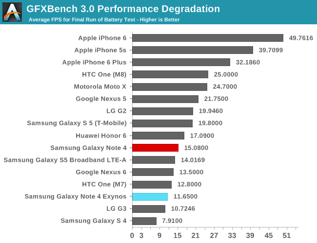
The performance degradation metric is exceptionally bad on the Exynos version. While the Snapdragon also has its thermal throttling issues, it seems to degrade much more gracefully than the Exynos. The Mali T760 is here limited to half its frequency during most of the benchmark run, spiking back to full frequency momentarily before throttling again. I'm disappointed to see such throttling behavior; it would've made much more sense to scale down to some of the higher frequencies first rather than dropping immediately to 350MHz.
The Exynos rendered 202K frames while the Snapdragon achieved 252K, 24.5% more. On the other hand the Exynos ran 18% longer. I have a feeling if both devices actually had similar throttling policies we would be seeing much closer scores in the end, taking into account screen power overhead.
All in all it seems the Qualcomm version has superior power management and is able to outpace the Exynos in day-to-day usage. I think this difference is not a matter of hardware efficiency differences but rather software oversights. The question is whether Samsung is willing to invest the time and effort into fixing their own SoC software, or if we'll see this pattern continue on for the foreseeable future.
Display Power
Until now we never really had the opportunity to take an in-depth look at a mobile phone's display power. This is particularly a problem in trying to characterize the power consumption and battery life of emissive screen technologies such as OLED. I went ahead and measured the device's power consumption at all its available brightness points and a few APL and grey-scale levels totalling 191 data points.
The x-axis represents the luminance measured at 100% APL throughout the device's 65 hardware brightness points, but the sunlight boost mode with auto brightness couldn't be included with this test. At 100% APL, meaning a full white screen, we see the power consumption rise up to 1.7W. The phone has a base power consumption of around 440mW when displaying a black screen, meaning the screen emission power to display white at 336 cd/m² of this particular device comes in at about 1.25W. The measurements were done in the sRGB accurate "Movie" screen mode; more saturated modes should increase the power usage due to the higher intensities on the OLEDs.
The power consumption seems to scale pretty linearly with luminance when using the device's brightness settings. However what is extremely interesting is how power scales with APL (Average Picture Level) and grey-scale level. Theoretically, an OLED's screen power should scale with APL and grey-scale level identically as a 70% grey-scale image is the same APL as an artificial 70% APL image. Here in our measurements we use APL samples consisting of pure white areas and pure black areas to achieve a target APL over the whole screen area.
Instead of our theoretical scenario, we see a huge discrepancy between a 70% APL pattern and a 70% grey-scale level image. This is due to how primary brightness and secondary luminance of color components are controlled in Samsung's AMOLED screens. I mentioned that power scaled more or less linearly when luminance is altered via the device's brightness controls. This is due to the panel increasing brightness by increasing the PWM cycle of all pixels on the panel.
In fact, if one had a high-speed camera or DSLR with fast enough shutter speed one could see and capture the rolling-shutter-like effect of how the panel is lit up: multiple horizontal stripes of pixels rolling from the top of the device towards the bottom in a similar fashion to how a CRT's electron beam behaves when moving in one axis. The brightness depends on the thickness of the stripes, or in other words how much active area is powered up vs inactive pixels. When looking from a single pixel's perspective, this results in nothing but a typical PWM pulse.
What remains to be answered is why we see a large difference in power when looking at the grey-scale power figures at equal APL as the APL pattern images. Although the primary brightness is controlled by PWM, the actual color output of each OLED is controlled via voltage. In my research in the past I've actually managed to retrieve the display driver IC's programmed voltage to see how the sub-pixels, and thus color, is actually controlled. Although I haven't looked into the Note 4's driver yet (it's an extremely time-consuming procedure), I had saved up the table of my old Galaxy S4:
If the Note 4's voltage curve behaves anywhere near the same, it's clear why an image containing white consumes more power than an equal homogeneous grey-scale picture with the same APL. There's a steep voltage increase towards the last few levels for each color component (white being 255 on all three RGB channels).
I am holding off trying to do any comparisons with LCD screens and past AMOLED generations as I still lack enough data points to make any educated statement on the power efficiency of the different technologies and panel generations. What can be said for certain is that the increasingly higher APL values, and especially white interfaces of Android, are AMOLED's Achilles' Heel. There's no doubt that we could see some very large power efficiency gains if UX design would try to minimize on colors nearing 100% saturation, which leaves some justification for the "grayscale mode" when using extreme power saving modes.
Charge Time
While Josh already tested the charge time on the Qualcomm version of the device, I wanted to add a charge graph comparing the two charge modes and add a little comment in regards to fast-charging.
The Exynos model supports the same fast-charging capabilities as the Qualcomm version - in fact many people have been calling this a feature enabled by Qualcomm's Snapdragon platform, or "Quick Charge", but that is only half correct. Both Note 4 variants' fast-charging mechanisms are enabled by Maxim Integrated's MAX77823 charger IC chip. The IC has been around for a bit but it has seen limited usage in only Japanese models of the Galaxy S5.
Samsung has not used Qualcomm's charger ICs in any of their recent products and always relied on Maxim solutions, even in combination with Snapdragon SoCs. What Qualcomm markets as Quick Charge is actually the proprietary signalling between the charger and a dedicated voltage switcher IC on the phone. What seems to be happening here is that although the Qualcomm device is advertised as QC2.0 compatible, it doesn't use it. Instead what appears to be implemented in the stock charger is Qnovo's Adaptive Fast Charging technology, which provides a similar solution.
The phone is able to detect if there's a 9V charger plugged in, enabling this charge mode if you enable it in the battery screen option, and it requires you to re-plug the device cable for the new mode to be active. The included charger supplies up to 1.67A at 9V, or 15W. Otherwise the normal charging mode takes place at 2A on 5V, or 10W.
We see in the fast-charging graph that the phone is being delivered just short of 11W of power up until the 75% capacity mark, after which the charger IC vastly limits the input power and gradually switches to trickle charging the device. The phone is able to be charged to 75% in just 50 minutes, which is quite amazing. A mere 15 minutes of charging on the fast charger can charge up to 25% of the battery. The total charging time in this mode is 138 minutes.
In the "slow" charging mode over a normal 5V charger, the device gets delivered around 7W of power up until the ~85% mark. Again the charger IC slows down the power gradually until the device reaches true 100% capacity. You will notice that the fuel-gauge will report 100% capacity much earlier than the input power reaching zero, but power continues for another 30 minutes after that. This is due to modern fuel-gauges faking the top few percent of a battery's capacity. Here it takes about 50 minutes to reach the 50% battery capacity mark, and a total of 171 minutes to truly fill up the battery.
Conclusion
Samsung's System LSI business had a rough two years as their decision to go with ARM's big.LITTLE SoC architecture cost them a lot of market share, thanks in part to immature software and implementation issues. Usually in the past Samsung's own Exynos SoCs were regarded as the more performant variant given the choice of Qualcomm's Scorpion CPU based solutions. This changed as the Exynos 5410 came out with a malfunctioning CCI, crippling the chip to the most battery inefficient operating mode of big.LITTLE.
Qualcomm's Snapdragon 800 capitalized on the new 28nm HPM manufacturing process, along with the advantage of being able to offer an integrated modem solution, and has dominated the market ever since. It's only now that Samsung is able to recover as the new 20nm manufacturing process allowed them to catch up and start to offer their own Exynos SoC in more variants of its products, a trend that I expect to continue in Samsung's future lineup.
The Note 4 with the Exynos 5433 is the first of a new generation, taking advantage of ARM's new ARMv8 cores. On the CPU side, there's no contest. The A53 and A57 architectures don't hold back in terms of performance, and routinely outperform the Snapdragon 805 by a considerable amount. This gap could even widen as the ecosystem adopts ARMv8 native applications and if Samsung decides to update the phone's software to an AArch64 stack. I still think the A57 is a tad too power hungry in this device, but as long as thermal management is able keep the phone's temperatures in reign, which it seems that it does, there's no real disadvantage to running them at such high clocks. The question is whether efficiency is where it should be. ARM promises that we'll be seeing much improved numbers in the future as licensees get more experience with the IP, something which we're looking forward to test.
On the GPU side, things are not as clear. The Mali T760 made a lot of advancements towards trying to catch up with the Adreno 420 but stopped just short of achieving that, leaving the Qualcomm chip a very small advantage. I still find it surprising that the Mali T760 is able to keep up at all while having only half the available memory bandwidth; things will get interesting once LPDDR4 devices come in the next few months to equalize things again between competing SoCs. Also ARM surprised us with quite a boost of GPU driver efficiency, something I didn't expect and which may have real-world performance implications that we might not see in our synthetic benchmarks.
It's the battery life aspect that I think it's most disappointing to me. It's a pity that Samsung didn't go through more effort to optimize the software stack in this regard. When you are able to take advantage of vertical integration and posses multi-billion dollar semiconductor manufacturing plants with what seem to be talented SoC design teams, it's critical to not skimp out on software. I might be a bit harsh here given that the battery disadvantage was just 12% in our web-browsing test and might be less in real-world usage, and the GPU battery efficiency seems neck-and-neck. Still, it's the wasted potential from a purely technical perspective that is disheartening.
This is definitely a wake-up call to ARM and their partners as well. If the software situation of big.LITTLE isn't improved soon I'm fearing that ship will have sailed away, as both Samsung and Qualcomm are working on their custom ARMv8 cores.
So the question is, is it still worth to try and get an Exynos variant over the Snapdragon one? I definitely think so. In everyday usage the Exynos variant is faster. The small battery disadvantage is more than outweighed by the increased performance of the new ARM cores.

