Original Link: https://www.anandtech.com/show/8557/x99-motherboard-roundup-asus-x99-deluxe-gigabyte-x99-ud7-ud5-asrock-x99-ws-msi-x99s-sli-plus-intel-haswell-e
The Intel Haswell-E X99 Motherboard Roundup with ASUS, GIGABYTE, ASRock and MSI
by Ian Cutress on September 25, 2014 11:30 AM EST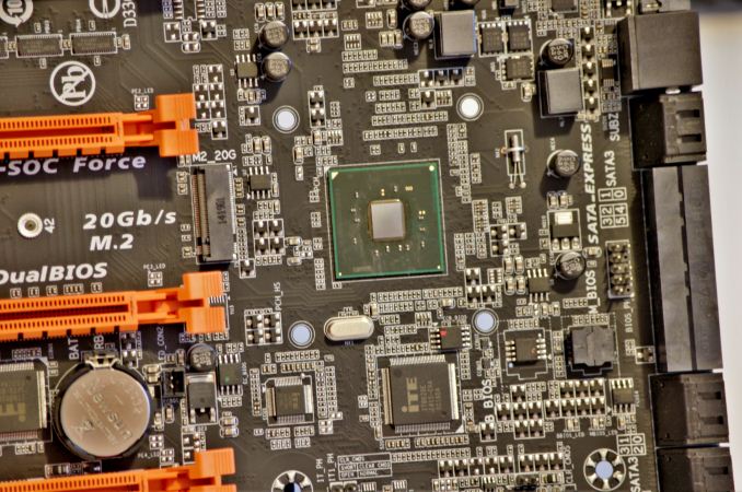
The launch of Haswell-E ushered in a triumvirate of new technology – a new CPU line, a new motherboard chipset and DDR4 memory. Today we focus on the new consumer motherboard chipset, X99, with motherboards from all four major manufacturers: the ASUS X99-Deluxe, the GIGABYTE X99-UD7 WiFi, the ASRock X99 WS and the MSI X99S SLI Plus. X99 represents the upgrade over the previous extreme chipset generation, X79, in several key areas in order to align itself better with the mainstream Z97 and Z87 platforms.
The X99 Chipset
Intel’s processor strategy at the high performance end of the spectrum ensures that the same line of motherboards with the same CPU socket and chipset are kept for two generations of CPUs. With the Nehalem and Westmere CPUs there was socket LGA1366 and the X58 chipset, and with Sandy Bridge-E/Ivy Bridge-E CPUs we had LGA2011-0 and the X79 chipset. This new line of Haswell-E processors (along with the future Broadwell-E ones) will use the LGA2011-3 socket and the X99 chipset. This means that users investing in the new Haswell-E processors must also invest in a new motherboard. This has several upsides in the levels of functionality.
For the first half of 2014, the zeitgeist of the X79 platform was centered on its age and the comparison to the newer Z87 and Z97 platforms aimed at the mainstream processor lines. The Z87 and Z97 chipsets afforded more native SATA 6 Gbps ports, more native USB 3.0 ports, PCIe based storage in the form of SATA Express and M.2 and more flexibility from the point of view of the manufacturers – the chipset had a certain amount of configurable input/output from the chipset to the motherboards could be designed with specific users in mind.
| Chipset Comparison | ||||
| X79 | Z87 | Z97 | X99 | |
| Launch Date | November 2011 | June 2013 | May 2014 | August 2014 |
| CPU Cores | 4 or 6 | 2 or 4 | 2 or 4 | 6 or 8 |
| PCIe Lanes | 40 | 16 | 16 | 28 or 40 |
| PCIe Configuration | 2x16 / 4x8 | 16, 8/8 | 16, 8/8, 8/4/4 | 2x16 / 5x8 |
| DRAM | Quad Channel DDR3 | Dual Channel DDR3 | Dual Channel DDR3 | Quad Channel DDR4 |
| TDP | 130W | 84W | 88W | 140W |
| Socket | LGA2011-0 | LGA1150 | LGA1150 | LGA2011-3 |
| SATA 6 Gbps | 2 | 6 | 6 | 10 |
| USB 3.0 | 0 | 6 | 6 | 6 |
| Thunderbolt Capable from CPU | No | No | Yes | Yes |
| Intel SRT/RST | No | Yes | Yes | Yes |
| PCIe Storage | No | Controller | Yes | Yes |
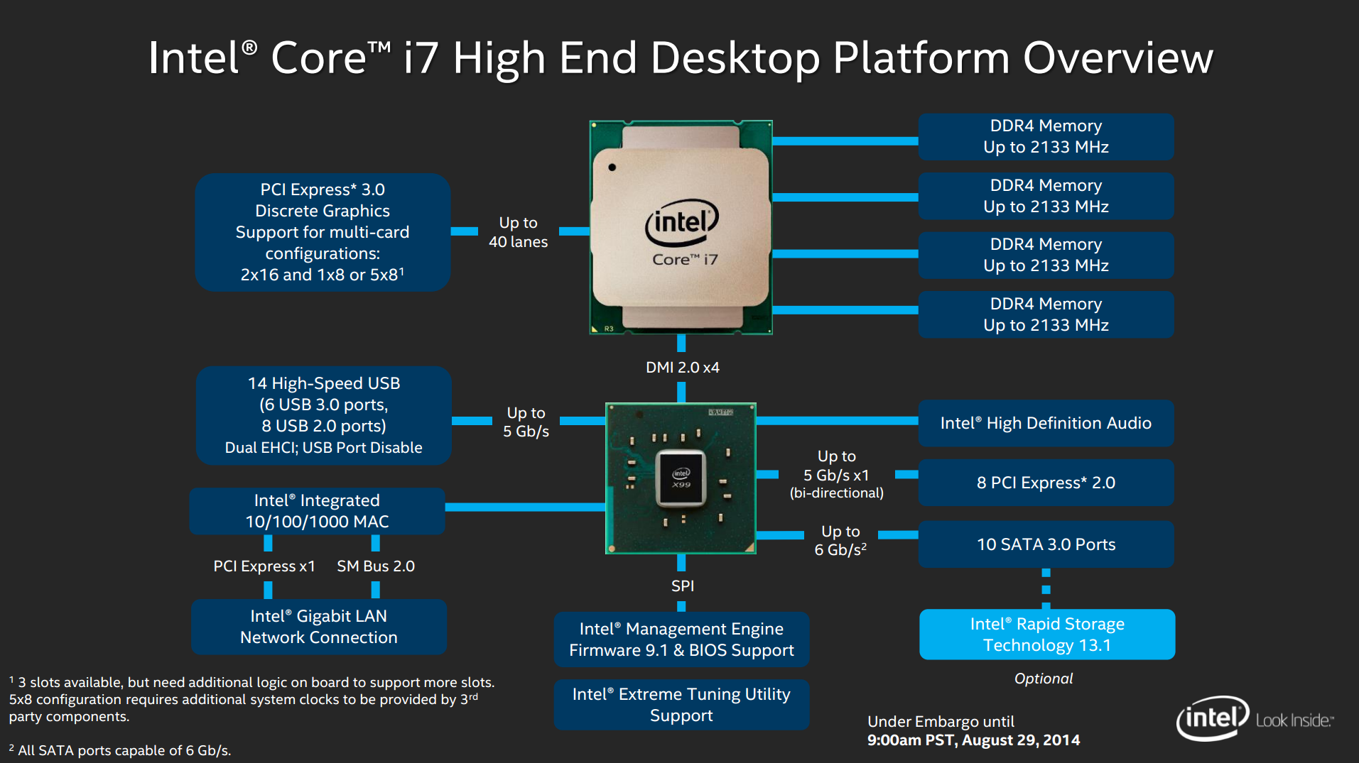
With X99, we get some significant upgrades all around. The chipset now supports ten SATA 6 Gbps ports natively, with six of those being RAID capable (more on this later). There is also up to six USB 3.0 ports native, direct Thunderbolt support and more possible PCIe configurations. The new PCIe storage options (SATA Express and M.2 via PCIe) are also both supported. The platform requires DDR4 compared to the older DDR3, but still retains forty PCIe 3.0 lanes from the CPU and eight PCIe 2.0 lanes from the chipset (in 8x1, 4x2 or 2x4 configurations).
PCIe Storage and Lane Allocation
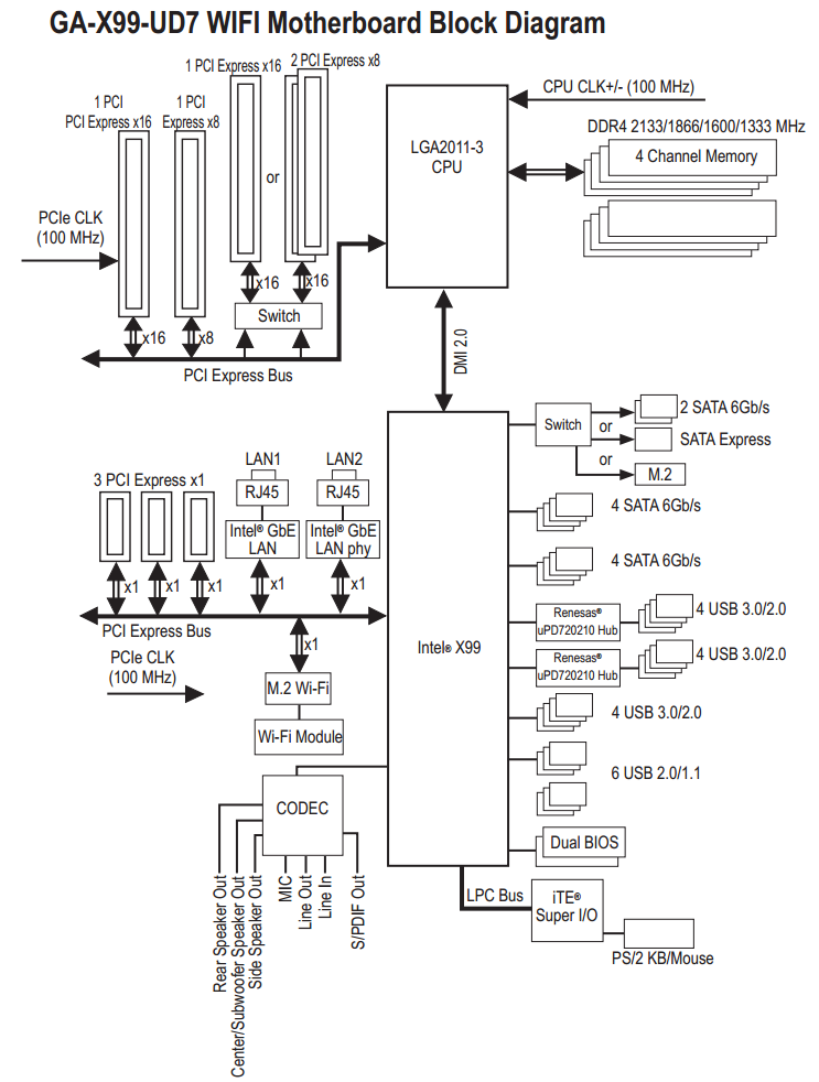
The inclusion of PCIe storage makes more sense for a platform like X99 as there seems to be PCIe bandwidth to spare. For each SATA Express connection, two PCIe lanes are required. For M.2 in PCIe mode, motherboard manufacturers can use two lanes or four lanes depending on the bandwidth they wish to support. With 40 lanes of CPU bandwidth, manufacturers need not use a PCIe 2.0 x4 slot from the chipset for three-way Crossfire support, giving extra free lanes to the chipset for these new storage technologies. Alternatively, some manufacturers are taking advantage of the CPU lanes and using four of these for an M.2 slot, as shown in this MSI chipset diagram:
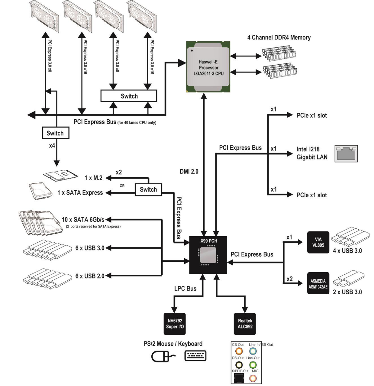
Here, four way GPU support is given by x8/x8/x16/x8, as it will be with most X99 motherboards, but the fourth PCIe slot can switch between a PCIe 3.0 x8 slot or a PCIe 3.0 x4 M.2 slot. This means that if the M.2 slot is used in PCIe 3.0 x4 mode, only 3x graphics can be used. But, to double up some potential confusion, the system can use M.2 slot in PCIe 2.0 x2 mode from the chipset, allowing four-way GPU configurations again.
This may seem complicated, but at the end of the day the extreme enthusiast can have either:
- 3x GPUs + PCIe 3.0 x4 M.2, or
- 4x GPUs + PCIe 2.0 x2 M.2.
This is such an excruciating decision to make (-sarcasm!). Joking aside, it is a clever solution to the PCIe storage issue if these drives ever get to market in significant number.
With regards to the SATA port situation, Intel is enabling ten SATA ports total but only six of them for RAID. While this is an update over X79, it seems more of a fudge. One would assume that it could be a bandwidth issue, because the link between the CPU and chipset (PCH) is at 20 Gbit/s, or 2.5 GBps which would be saturated by a 5-6 disk RAID-0 array. However, it seems silly to not have RAID on four of those ports. Due to Intel’s previous flex-IO arrangement on Z97, this seems more of an integrated SATA 6 Gbps hub, splitting the bandwidth into four ports. Due to the hub it would limit throughput in RAID so it makes sense to disable it completely for those ports. Intel is telling us that this is due to two separate AHCI controllers in the chipset, with only one of the AHCI controllers enabled for RAID.
For motherboard manufacturers, this gives several options. If the chipset is using Flex-IO which we believe it is (we are still awaiting confirmation), then the amount of SATA 6 Gbps/USB 3.0/PCIe 2.0 lanes is slightly flexible similar to Z97. By providing 10 possible SATA 6 Gbps ports (6+4 of RAID/non-RAID), the motherboard manufacturer could implement a 4+4 arrangement to give more PCIe lanes, or shift around the PCIe lanes in that 4+4 to give a full six USB 3.0 ports. The truth of the matter is that there are very few users who require a six-drive RAID, and so motherboard manufacturers can target different orientations of motherboards for different user segments. The non-RAID possible ports are still fine for optical storage or hard drives with a software RAID-1 applied over the top.
The PCIe Arrangement – 40 or 28 PCIe lanes?
In Intel’s chipset platform overview above, it states that for up to 40 lane CPUs, multi-card configurations are available as 2x16 + 1x8 or 5x8 configurations. There are two interesting points to note here, and the first is the implementation of 5x8.
In the bottom of this slide it shows the following:

In the MSI chipset diagram above, we see that in order to get x8/x8/x16/x8, an additional switch is used such that one of the x16 can be split into x8/x8. Although GIGABYTE claim that it is not that simple, and without an external clock generator (as mentioned in the image above) motherboards may be limited to x8/x8/x8/x8:
Given the pricing of X99 motherboards ($240-$500), one would hope that all manufacturers who are aiming at a four-way GPU design specifically for gaming or PCIe limited compute would implement the single full x16 alongside the trio of x8 slots for quad-PCIe devices.
The second issue to arise from PCIe lane allocation derives from the CPUs themselves. While some X99 motherboards will support Xeons, all the LGA2011-3 oriented CPUs will feature 40 PCIe 3.0 lanes except the Core i7-5820K, which will only support 28. As a result, instead of x16/x16 gaming for two-way GPUs, 5820K users will have x16/x8. As we tested in our CPU review of the Haswell-E consumer processors, for two-way SLI gaming at 1080p, this has almost zero effect on actual frame rates. The 5820K is also limited in three-way GPU gaming, offering x8/x8/x8 rather than x16/x16/x8, and cannot be used for four-way SLI gaming without the addition of a PLX chip. On the motherboard side, this means that manufacturers have to cater for both 28 PCIe lane processors and 40 PCIe lane ones as well.
Normally, the 40 PCIe lane processors will use the PCIe slots in typical fashion, however users are recommended to look into the manual for three-way implementation. For example, the ASRock X99 WS in this review gives the following:
| ASRock X99 WS | 1 GPU | 2 GPUs | 3 GPUs | 4 GPUs |
| 40 PCIe 3.0 | x16/-/-/-/- | x16/-/-/x16/- | x8/x8/-/x16/- | x8/x8/-/x8/x8 |
| 28 PCIe 3.0 | x16/-/-/-/- | x16/-/-/x8/- | x8/x8/-/x8/- |
This gives both orientations the same sequence of adding in graphics cards, but users should look in the manual to find out the best way. For our X99 reviews, we will try to aid this in our board specifications tables. As a feature, ASUS has added a series of LEDs connected to an ‘SLI/CFX Switch’ that light up the LEDs next to the PCIe slots to use for 2x and 3x GPU configurations:
The DDR4 Conundrum
As we will explain in our DDR4 coverage, this new platform is a boon for DRAM manufacturers and resellers. Each new computer needs a new memory kit and cannot simply recycle the old DDR3 into a new build.
Almost all motherboards will support either one or two DIMMs per channel, giving a maximum of 64GB of DRAM using 8 GB modules – this does not change anything from X79 then, except the DDR4 itself being lower voltage and different sub-timings. X99 also puts in extra provisions for internal testing – on the first POST with new memory detected, or a change in the DRAM speed, the system will spend a few seconds stress testing the memory in order to find if the settings are out of step. The only potential spanner in the works regarding compatibility is the timing of the launch.
The original date for the release of Haswell-E and X99 was during IDF, on the 9-11th of September. Everyone had their schedules locked in for those dates, but when Intel bought the release date to two weeks earlier than expected, panic (almost) ensued. The motherboard manufacturers were there or there about with their products, as typically the last few weeks are dedicated to compatibility testing with memory. However the memory manufacturers were still organizing their product lines and module categories.
As a result, the motherboard manufacturers were not as prepared as usual to qualify all the memory ready to go on sale (this has been fixed now with the latest BIOS updates) and memory manufacturers are still putting kits together. Combined with the high price of DDR4 and the initial limited quantity, prices for DDR4 were particularly high: $250 for 16GB as we noted at Haswell-E launch.
Memory manufacturers are still preparing kits, and motherboard manufacturers are continuously updating their qualified lists. With all the memory kits I have in to test, I have not had a motherboard not POST because of it, however in order to get the best performance out of that new high end memory kit (2666 MHz+), BIOS updates should be the number one priority. Most manufacturers have software that can do this (MSI’s Live Update 6) or users can download and update manually. Navigating to a BIOS update via the motherboard manufacturer website might show something like:
X99-DELUXE BIOS 0801: 3. Improve XMP settings
X99-UD7 WiFi BIOS F7b: 2. Improve DDR4 3000&2800MHz 4Gx4 compatibility
This happens throughout the lifetime of the product, and keeping up to date if you purchase a DDR4-3000 kit is vital.
I want to touch on voltages here as well, because although 1.2 volts is the standard for DDR4, there are two other voltage modes for memory on the platform:
| DRAM Comparison | |||
|
Low Voltage |
Standard Voltage |
Performance Voltage |
|
| DDR | 1.80 V | 2.50 V | |
| DDR2 | 1.80 V | 1.90 V | |
| DDR3 | 1.35 V | 1.50 V | 1.65 V |
| DDR4 | 1.05 V | 1.20 V | 1.35 V |
Low voltage modules will be placed at 1.05 volts in order to draw less power, but might be limited on speed. High performance modules (typically DDR4-2666 or higher) will run at 1.35 volts, which is an identical swing in the other direction. 1.35 volts for a high end memory kit is reasonable and should not affect longevity of the platform.
The Motherboard Market
As it stands, almost all the motherboard manufacturers announced a number of X99 models, with about half ready to go on day one, and the rest to trickle through over the next few months. These will be the core motherboards through Haswell-E and Broadwell-E, although we might see a partial update nearer Broadwell-E launch.
The following have been announced or are on offer:
| Motherboard Price List | |
| Price | Motherboard |
| $600 | ASUS Z10PE-D8 WS |
| $520 | ASUS X99-E WS |
| $500 | ASUS Rampage V Extreme |
| $429 | MSI X99S Gaming 9 |
| $400 | MSI X99S Xpower AC |
| $400 | EVGA X99 Classified |
| $400 | ASUS X99-Deluxe |
| $350 | GIGABYTE X99-SOC Force |
| $345 | GIGABYTE X99-Gaming G1 |
| $330 | ASRock X99 OC Formula |
| ~$325 | ASUS X99-Pro |
| $323 | ASRock X99 WS |
| $310 | GIGABYTE X99-UD7 WiFi |
| $300 | EVGA X99 FTW |
| $298 | GIGABYTE X99-UD5 WiFi |
| $294 | GB X99 Gaming 5 |
| $289 | MSI X99S Gaming 7 |
| $285 | ASRock X99X Killer |
| $280 | ASRock X99 Extreme6 |
| $280 | ASUS X99-A |
| $259 | GIGABYTE X99-UD4 |
| $250 | EVGA X99 Micro |
| $250 | ASRock X99M Killer |
| $245 | GIGABYTE X99-UD3 |
| $239 | ASRock X99 Extreme4 |
| $229 | MSI X99S SLI Plus |
| $224 | ASRock X99M Extreme4 |
| $210 | ASRock X99 Extreme3 |
Prices range from $500+ (ASUS Rampage V Extreme) to $210 (ASRock X99 Extreme3) although we might see one or two higher than this (ASRock X99 Extreme11, maybe) depending on the final configurations. Note that this is cheaper than Nehalem with X58 when a motherboard reached $700 or with X79 when the Extreme11 was around $600.
I Saw a Thing On Burning Motherboards
Two review websites have reported their X99 motherboards failing since the launch.
Nathan at Legit Reviews was testing high performance memory above the recommended voltage range (1.50 volts) on an ASUS X99 Deluxe and upon changing memory kits it seems that the power delivery to the CPU failed. The power delivery is solely for the VCIN to the FIVR, and thus unconnected to the memory, and it would seem that a large amount of heat caused a burning smell and some solder to move on the motherboard.
Michael at Phoronix had built a system (5960X + MSI X99S SLI Plus) from the ground up and at the point where the machine was first turned on, the chipset failed with a spark and a second issue with the power delivery occurred.
There are a couple of issues worth mentioning here. Nathan at LR was using his review sample that came direct from ASUS, whereas Michael at Phoronix was using a purchased motherboard from Newegg. Both of these would have been from the initial batches of motherboards that come from their respective factories, and while failures are uncommon they do happen: perhaps more so with the first batch out of the factory.
Nathan’s sample seems to have passed through a lot of testing already, whereas Michael’s sample went kaput on turn-on, suggesting more of a failed component rather than anything systemic. It seems unfortunate for the platform that two review websites have both had failures in a short space of time, and substantial failures at that.
I have had failures in the past (Bluetooth adaptor shorting out, DRAM or PCIe slots not working, PSU going BANG… twice) however these tend to be the exception rather than the rule. As with any product, there is a failure rate. I would be more concerned with Nathan’s issue, although it may just have been a sample with a lower weak point than most. When Rajinder was testing motherboards at AnandTech under liquid nitrogen, it particularly showed some of these issues.
Both of these X99 failures are nothing compared to the P55 socket burn issue that occurred back in 2009.
One potential explanation afforded for the failures has been the relatively high current draw for Haswell-E CPUs. When overclocked these CPUs will draw 25 amps from the 8-pin CPU power connector, and thus a good power supply is recommended. Even though that represents an overclocked system, at stock the draw is still high which could lead to unexpected spikes. Nathan noted that the over-current protection (OCP) was being triggered during his failure, and other users are pointing to the single 8-pin CPU connector to blame, rather than having two.
We have both the ASUS X99 Deluxe and the MSI X99S SLI Plus in this review, from those initial batches that were manufactured, and have experienced none of the issues raised. Our ASUS X99 Deluxe has also been through some high speed memory testing as well as CPU overclocking and 160W Xeon testing without issue. Our one data point is invariably anecdotal as best, although if this is a more prominent issue I would assume we would have seen more failures in a consistent circumstance. If something does arise, we will post something about it.
This Review
Today we focus on some of the more exciting motherboards out in the market in the first of our X99 coverage articles. Due to the way the motherboard manufacturers were sampling for X99, we were unable to align several motherboards of a similar price. However one motherboard is a high end part, one is aimed at workstations and another strikes at a nice low price point to provide a contrast. The final one sits in the middle of the price bracket but also at the top of its product stack. We have in to test:
ASUS X99-Deluxe: $400
GIGABYTE X99-UD7 WiFi: $310
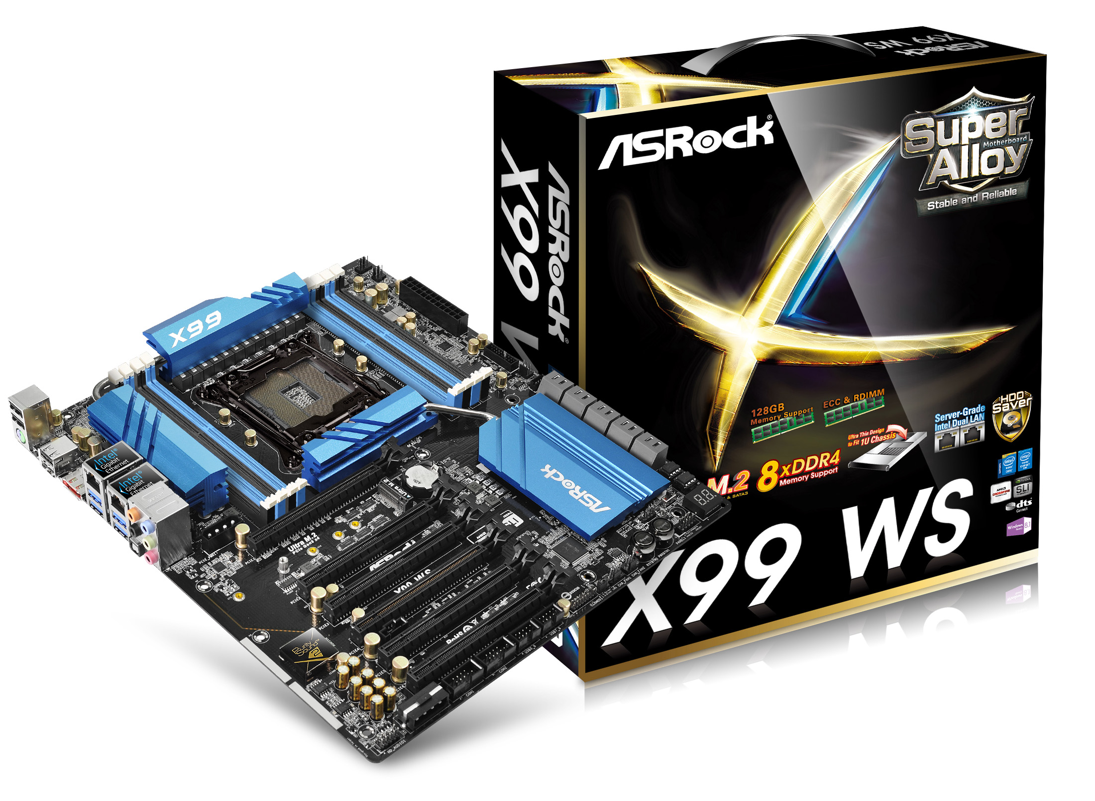
ASRock X99 WS: $324
MSI X99S SLI Plus: $229
The Deluxe and UD7 are typically the top of the range for the ‘channel’ line of motherboards (compared to the Gaming/OC ranges), and ASRock’s WS nomenclature is representative of the workstation-like attitude they have taken to this model. MSI’s name of ‘X99S’ indicates SATA Express connectivity, while the SLI Plus itself is oriented towards gamers but in a budget build.
ASUS X99-Deluxe: The New
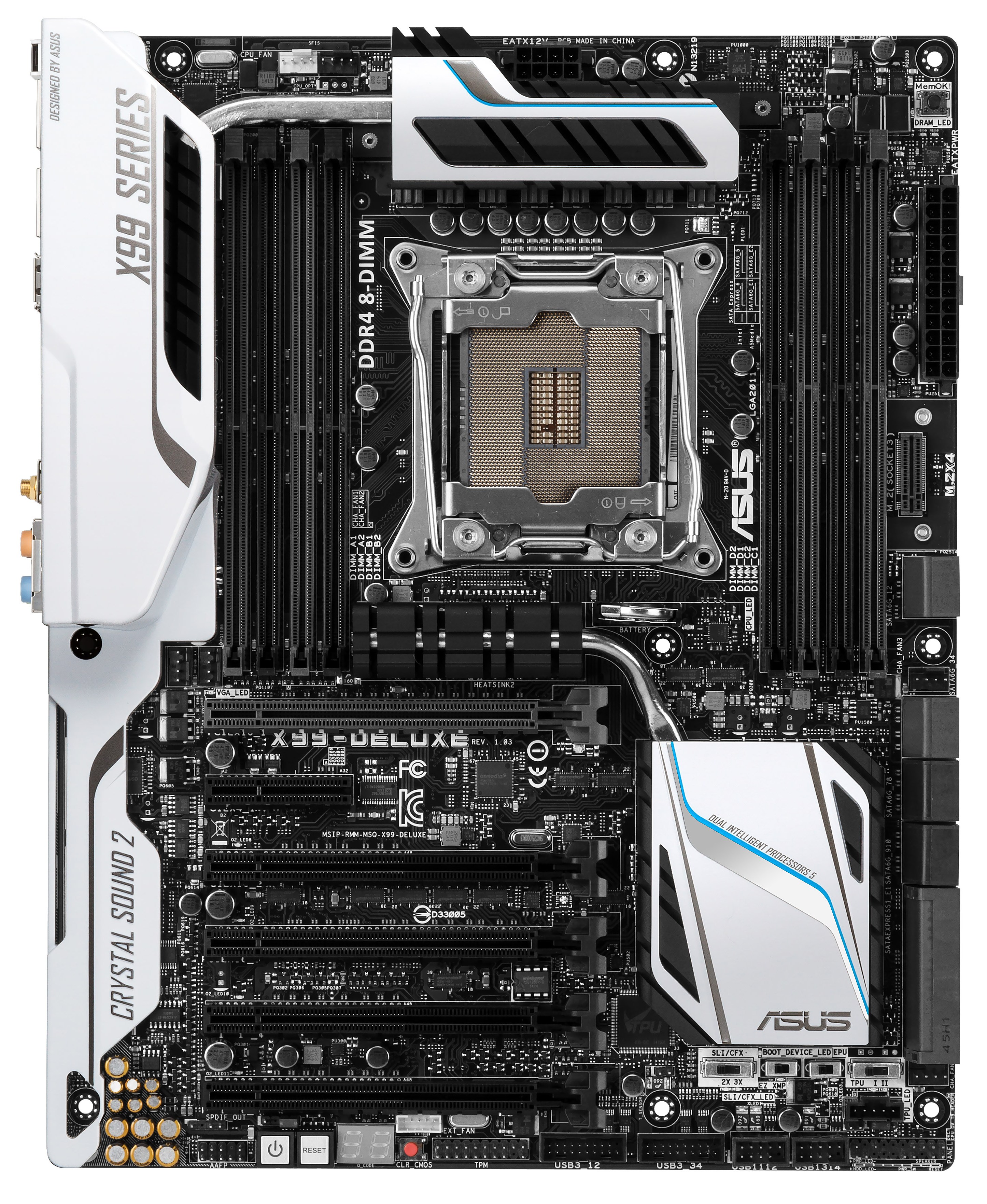
What color works best for a motherboard? ASUS has been playing around this idea for several generations, offering blue, red, brown, gold and grey in recent times for their various channel/gaming/TUF ranges. But now the buck gets passed on to a white livery featuring a long protective shield reaching from the IO down to the bottom of the motherboard to improve the overall look. The power delivery heatsink at the top and the chipset heatsink both continue the theme, with the extra space between the CPU and PCIe slots used for a third but black heatsink. The slots and SATA ports are a combination of black and grey. This is the first motherboard in recent history to play with a black and white theme, allowing system modifiers (who often target high performance systems) to be liberal in how they style their creations.
For X99 ASUS has upgraded its hardware prowess in several key areas. The first one to tackle is the one that seems to be most talked about: the ASUS OC Socket.
The principle behind the OC Socket is this: some of the pads on your LGA2011-v3 processor are not designed for normal use. They are either not listed in the motherboard manufacturers guides or are used as internal diagnostic aids (either Intel only or for motherboard manufacturers as well). With these extra pads motherboard manufacturers can probe certain parts of the CPU for pre-testing but then in the retail versions of the socket there are no pins to mess around with. Intel validates the CPU for use with certain pins, with the unlabeled or diagnostic or pins always in a state of ‘beta/never fully validated’ type miasma.
What ASUS has done is equipped the ‘OC Socket’ with some of those pins, and then by using proprietary circuitry claim to offer extended performance in both extreme CPU overclocking and memory overclocking.
What exactly ASUS has done is not 100% clear in function, although it should be obvious that these pins are not for adding in voltage. (Voltage is always routed via the FIVR on Haswell/Haswell-E, so there is not a way of getting more into the system. Plus, the BIOS already can add voltage by adjusting numbers.) ASUS is patenting the socket design in order to stop others using their innovation. What could be happening is akin to an internal adjustment, allowing extra parameters to be used. For example, if you are old enough to remember the Commodore C64, the 6581 SID (audio) chip could have certain voltage levels adjusted to enable an extra virtual audio channel beyond the design specifications. ASUS is keeping quiet on what the OC socket specifically does, at least until the patent clears.
There have been some worries about whether this OC Socket is a valid design improvement recognized by Intel. Because it adjusts the way the CPU interacts outside normal specifications, there has been a worry that Intel will not honor warranties. Intel’s official stance to media in general so far for modifications is that:
‘our partners consistently deliver innovations … for questions on specific 3rd party products and their implementation, please contact them’
That specific phrasing does not swing either way as affirming or denying the specific situation, no matter how some journalists interpret that wording. Until Intel provides an official report into the OC socket, to extrapolate extra meaning or declare the situation resolved without a line referring specifically to the technology is erroneous.
Our verdict on the OC Socket is this: ASUS has stated that these pins do not deliver extra voltage to the CPU (makes sense, as that is taken care by the FIVR) but open up additional functionality to extend overclocking margins. Intel stated directly via email to us that ‘of course when overclocking all warranties are void’, and given ASUS’ explanation of the feature it which suggests that the effect of the OC socket is essentially zero at stock speeds. So even if the CPU goes kaput in the ASUS motherboard (at stock), Intel will most likely honor the warranty. Although an official statement from Intel would clear up the matter. Given how infrequently CPUs are DOA at stock, this should not be an issue for any users picking up an X99-Deluxe today.
Next is the SLI/Crossfire switch that indicates which PCIe slots should be used for multi-GPU setups:
ASUS’ technical PR mentioned that this feature was added because one common question on the ASUS/ROG forums was ‘where do I put my 2nd/3rd graphics card’? This information is always in the manual, however in order to aid users straight away, a small switch was added under the chipset to light up these LEDs next to the slots. Note that this switch only turns the LEDs on and off – when I saw the feature I assumed it also adjust PCIe lane assignments, but I can confirm that it is more a dumb switch as it still requires the user to place the cards in the right place.
The next new feature is one I am very happy to see on a motherboard. Users who follow my Twitter may have noticed that over time I often reminisce about increasing the networking throughput on the motherboard – usually by upgrading to 10G-BaseT. However there is another way to increase bandwidth: more cowbell WiFi. For the X99 Deluxe, ASUS has equipped the system with a 3T3R 802.11ac WiFi card via mini-PCIe, allowing for connection speeds up to 1300 Mbps:
Note that this requires a 3T3R capable router to get the full performance, which depending on where you are in the world might be hard to find. I asked about what the price difference between the 2T2R 802.11ac module found on previous motherboards and this add-in would be, and the best answers I could find were in the +50% range. I am hopeful for the future that this comes down however, given that 2T2R solutions are the standard on any new motherboard that uses WiFi. It may be that the upgrade to 3T3R allows motherboard manufacturers to make that distinction with their high end models (like what ASUS is doing).
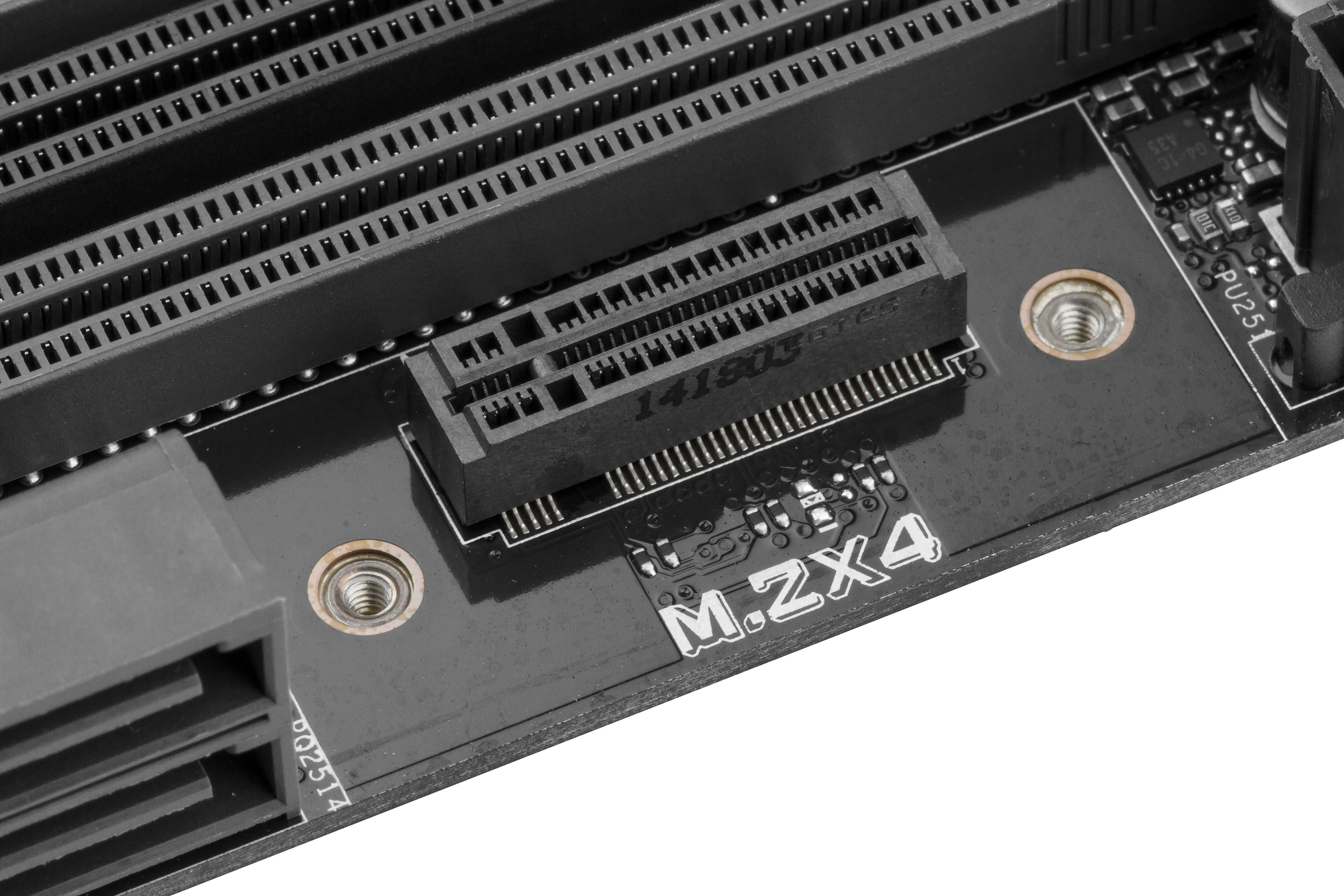
ASUS is also tackling PCIe storage head on. They were the first company to experiment with SATA Express, and Kristian tested ASUS’ first implementation back in March. Since then we have had the mainstream Z97 chipset which is awash with SATAe and M.2 connectivity. For X99, Intel has added support for PCIe storage, and ASUS here has gone with both M.2 and SATAe, although the M.2 solution is a little different to normal. With the X99-Deluxe, bundled in the box is a Hyper M.2 x4 card allowing for M.2 drives up to 22x110 but specifically to be placed into one of the PCIe slots on board:
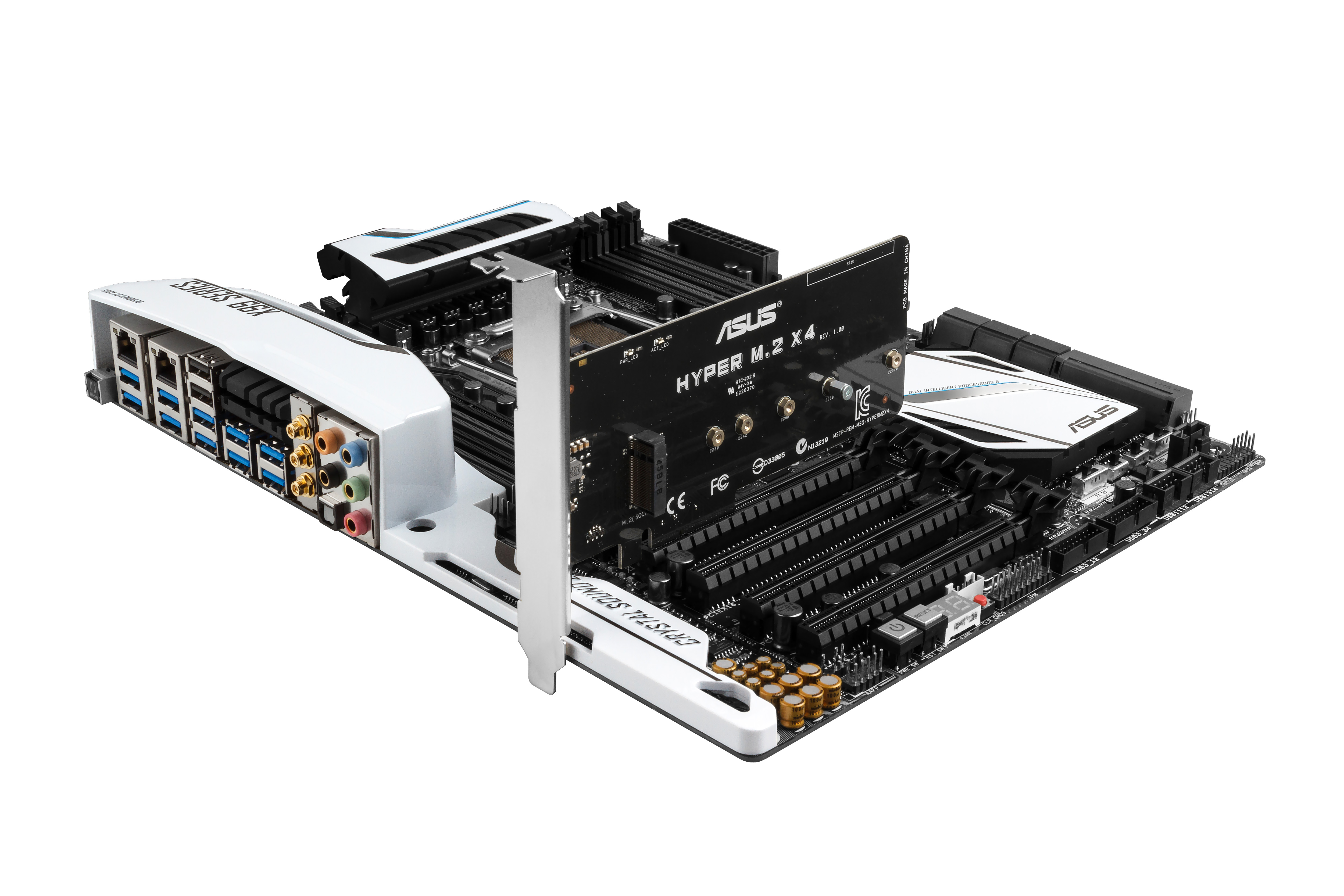
The card itself is just an M.2 slot that has pathways through the PCIe layer. We saw this card back at Computex, and it looks to be another differentiation point for ASUS’ high end.
That is not all to the M.2 story, as ASUS went slightly crazy and also installed a vertical M.2 x4 slot. Yes, you read that correctly.
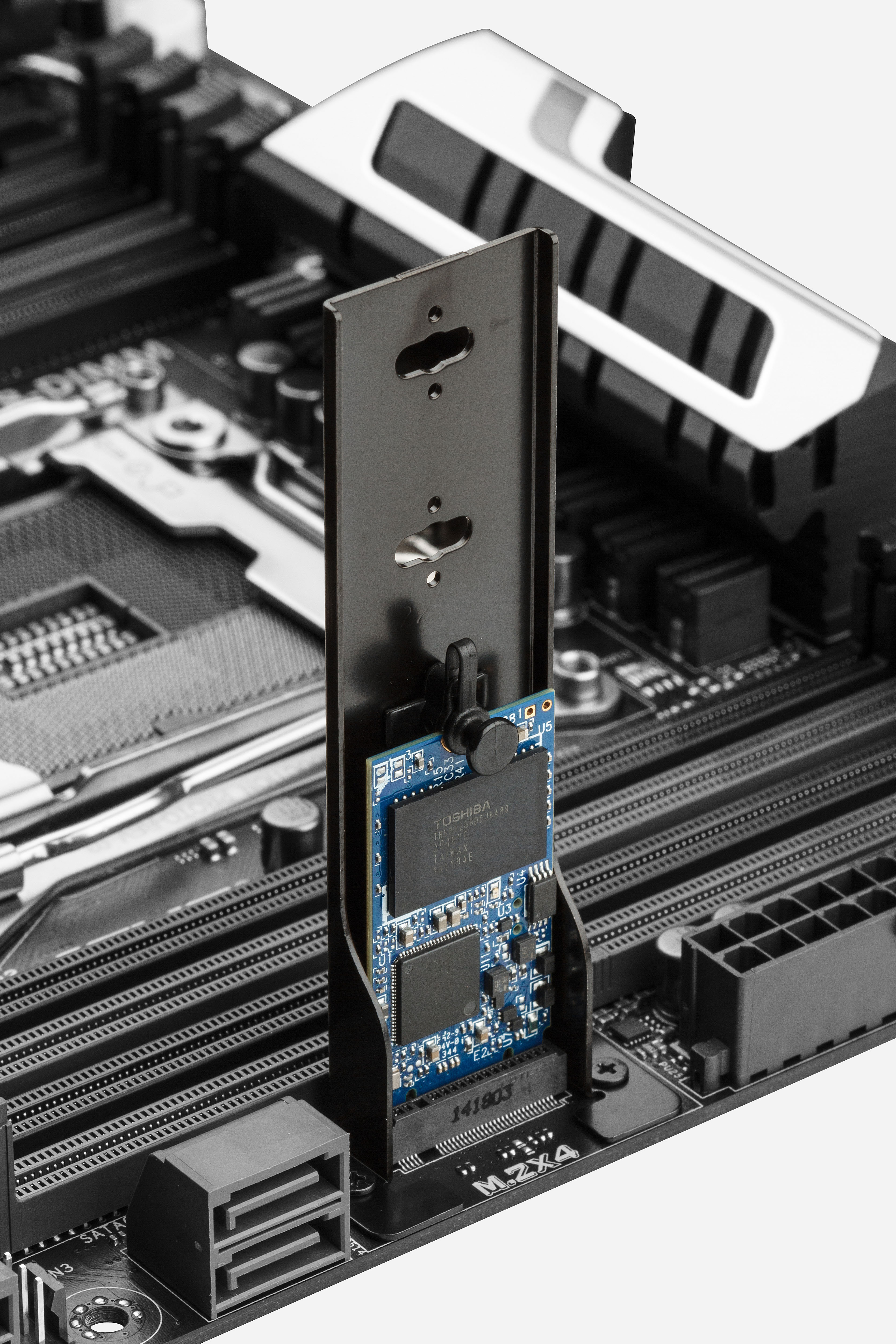
In the area normally reserved for termination resistors and other electronics, ASUS placed a pad and included a bracket for an M.2 drive up to 2280 to be used in PCIe 3.0 x4 mode.
So while this new feature springs out of the motherboard by 8-10cm, CPU heatsinks are often taller than this. As a result, the device might adjust the airflow around a small portion of the motherboard. Users who enjoy tidy cable management might be affected as well, depending on how you like to make the system light up. I could see a modder adorning this latch with LEDs to make some rainbow motif.
SATA Express is also in force, with a combination of Intel and ASMedia ports for two drives. When not in use, this gives the motherboard a total of 12 SATA ports: 10 from the chipset (6 RAID capable) and two from the ASMedia controller.
Next in the bag of tricks is regarding the fan headers. It would seem that ASUS has had requests for more than the 6 fan headers it normally places on the high end products. ASUS recently upgraded most of its range so that all the fan headers would accept DC or PWM fan control, but now system modders just want more of them. With the Rampage IV Black Edition, this was provided by the bundled OC panel, however with the channel motherboard, ASUS has included an extra movable PCB to offer extra headers:
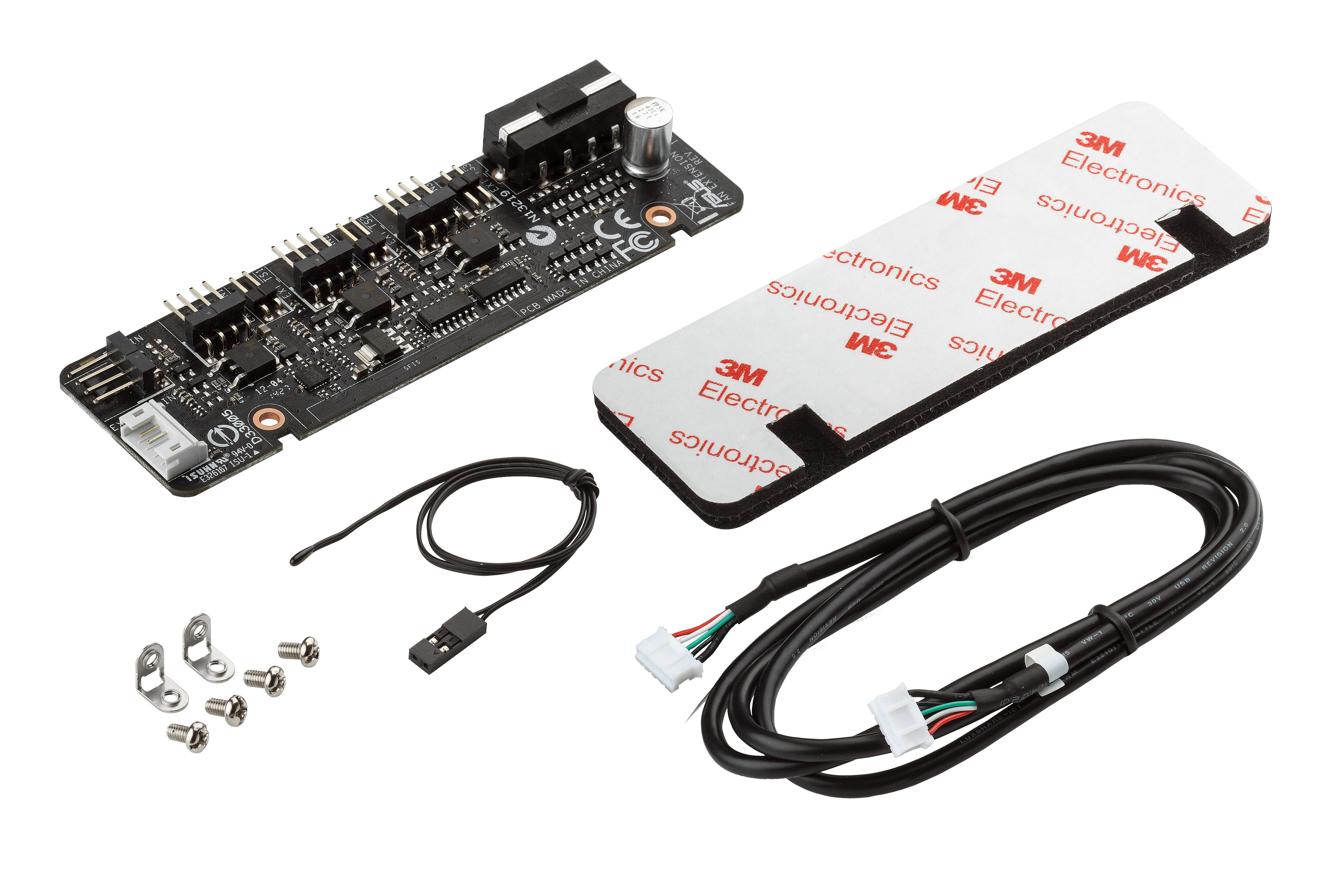
Here we get a PCB that requires one molex connector for power to give three extra fan-out headers with one fan-in. It requires the white dual ended cable to be connected to motherboard in order to pass on information and adjust fan profiles, and the big 3M thing is a double sided sticky pad to affix the fan controller card to a case if the screws are not used. The cable in the middle is a thermistor, providing an extra temperature reading when placed in the controller card and can be adjusted around the case so users can customize their fan responses. This gives the motherboard a total of nine fan headers. I would not be surprised if this extends out to other motherboards as a way to save PCB space, although it might be interesting if ASUS offered a way to bolt it on to the Hyper M.2 card or offer a combination card.
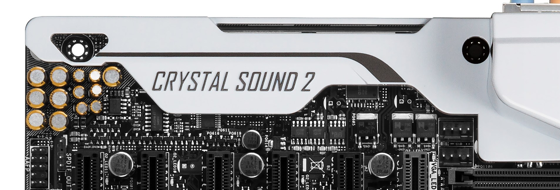
The final new major hardware element change for the X99-Deluxe is the audio system. Having seen first-hand how ASUS test the audio, at the time I got talking to the engineers about what aspects of audio they care most about and how they go about creating better audio. The results of their efforts have been piled into Crystal Sound 2, which uses updated versions of shielding, EMI protection, PCB separation, amplifiers, de-pop circuits and impedance detection methods. One of the features mentioned to me back at ASUS’ HQ is that they are prepared to add in components to improve the frequency response at the low end (a common issue for digital audio) even if it means shaving off a few dB from the peak dynamic range results.

The Overview
Aside from all the new stuff, anyone used to an X79 motherboard will feel right at home with an X99 unit. The socket levers are slightly different, requiring the lever to be pushed in then up, rather than out then up. Due to the LGA2011-3 designation, all LGA2011-0 coolers will work because the screw holes for coolers are all in the same place. There are technically two versions of the LGA2011-3 socket, although we will only see this square version on consumer motherboards – the other ‘narrow’ classification is more for server products.
On the X99-Deluxe we have already mentioned the white heatsinks, with ASUS using heatpipe connected heatsinks to create two pairs of cooling surfaces. We get the full complement of DRAM slots, and the CPU socket has a single 8-pin power connector. There are four fan headers immediately around the socket – two CPU headers in the top left and two on the bottom left. A fifth is slightly further away between the SATA ports on the right, and a sixth is underneath the SATA ports.
The right hand side has the MemOK button, followed by the 24-pin ATX power connector and the vertical M.2 x4 slot. The SATA arrangement follows, with the following combination:
The four SATA 6 Gbps ports in grey at the top are RAID capable.
The four SATA 6 Gbps ports in black underneath these are not RAID capable.
The other SATA ports are in the SATAe complex:
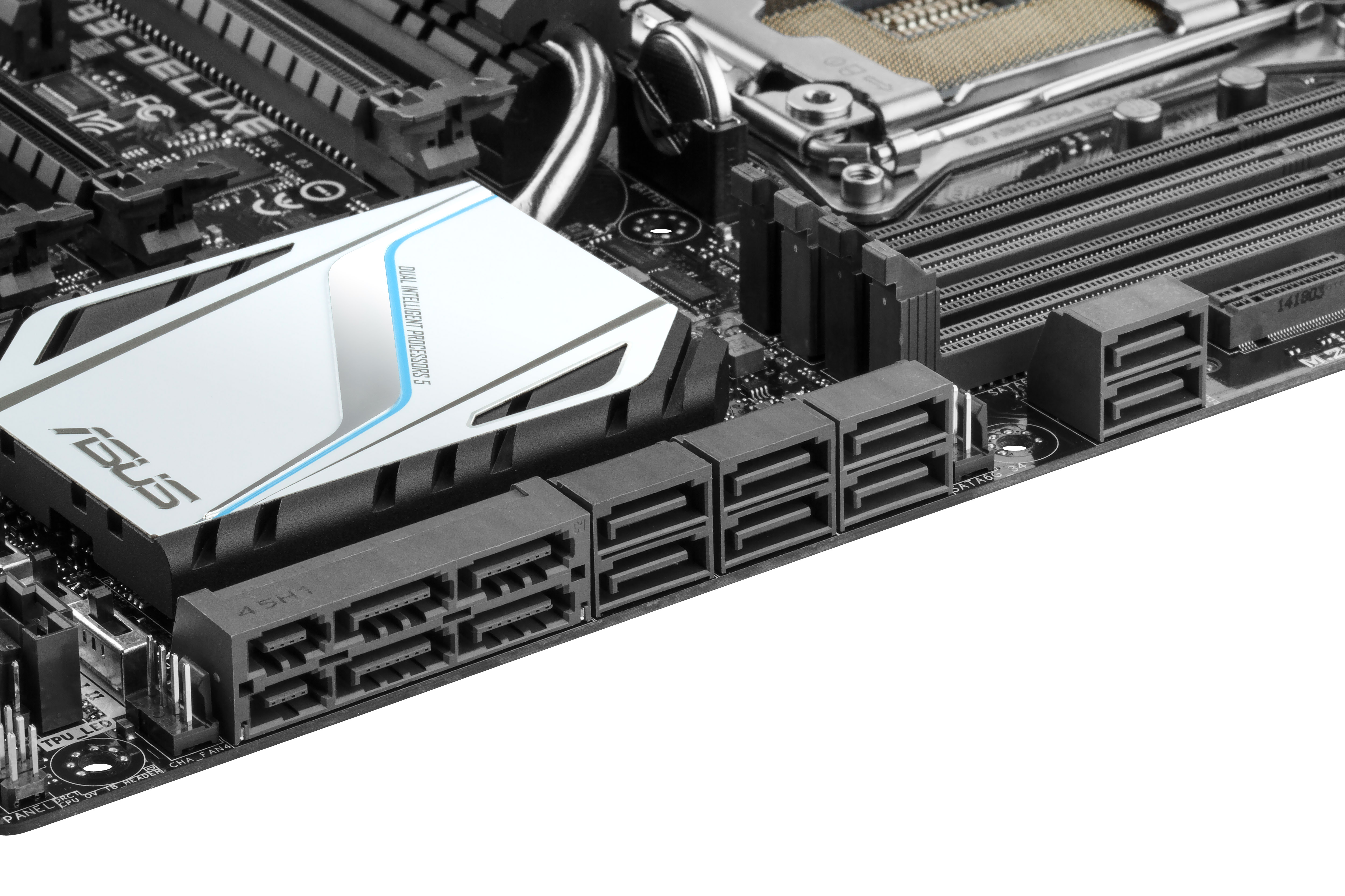
The top SATAe section is powered by the Intel X99 Chipset, and these SATA ports are RAID capable. The bottom SATAe is powered by the ASMedia controller, and it is suggested that only data-based hard drives are used in the SATA ports.
Confused yet? The safest way to look at it is the top four are for RAID, and the rest is for anything else, except the bottom two SATA ports in the SATAe block which should not be used for optical drives.
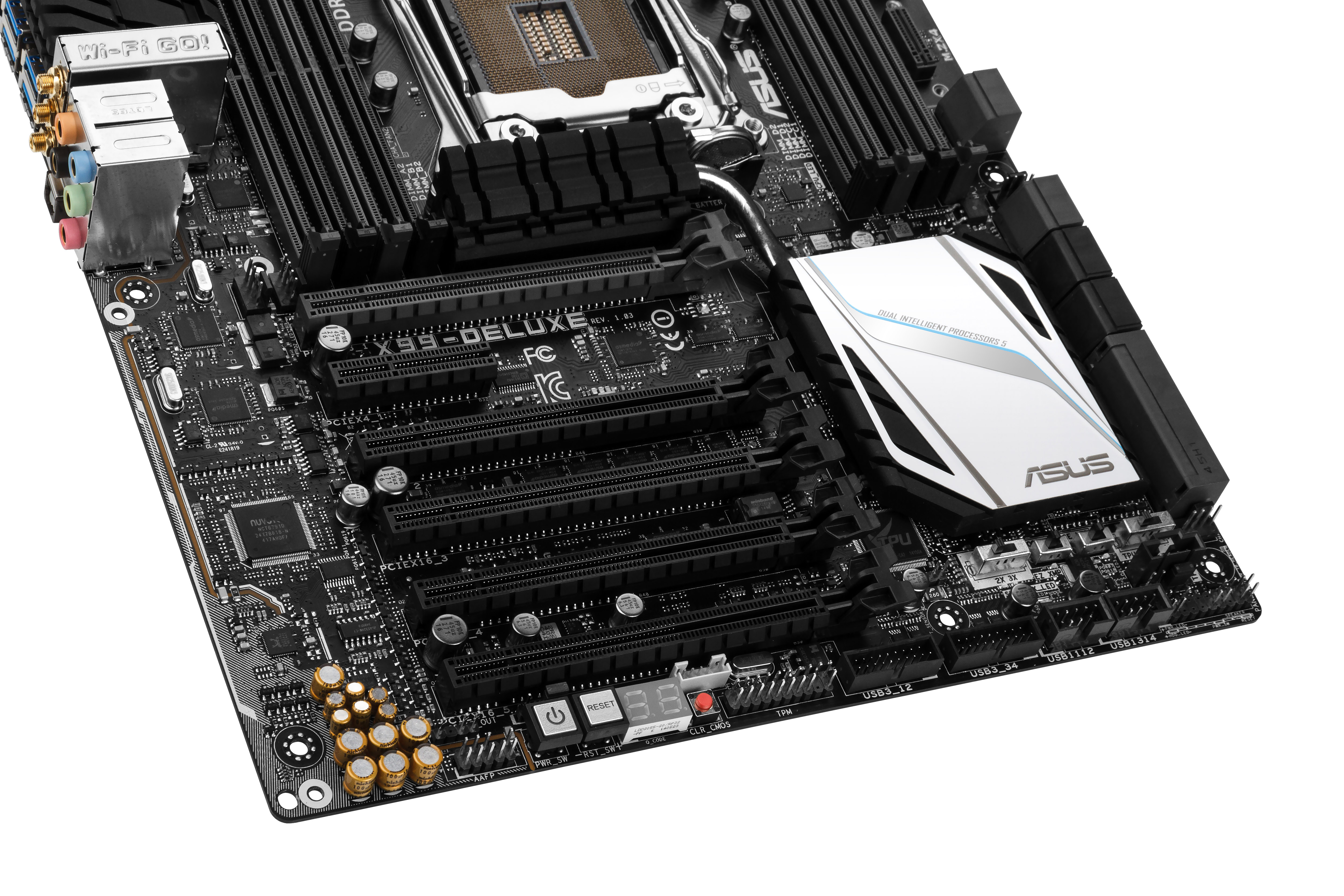
The bottom of the motherboard is also a mélange of headers and switches. Underneath the chipset heatsink we have the following:
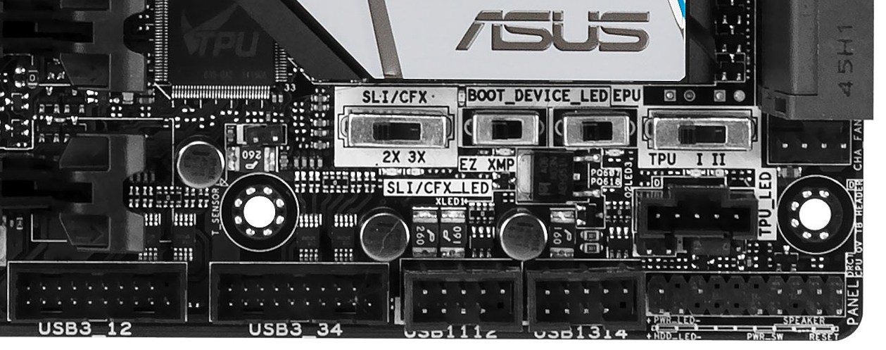
The SLI/CFX switch, as mentioned above, enables LEDs next to the appropriate PCIe slots for 2x and 3x operation. The switch to the right of this is the EZ XMP switch, which tells the motherboard to enable the high speed memory installed. Next is the EPU switch for power saving, and finally a two-stage TPU offering two types of overclock.
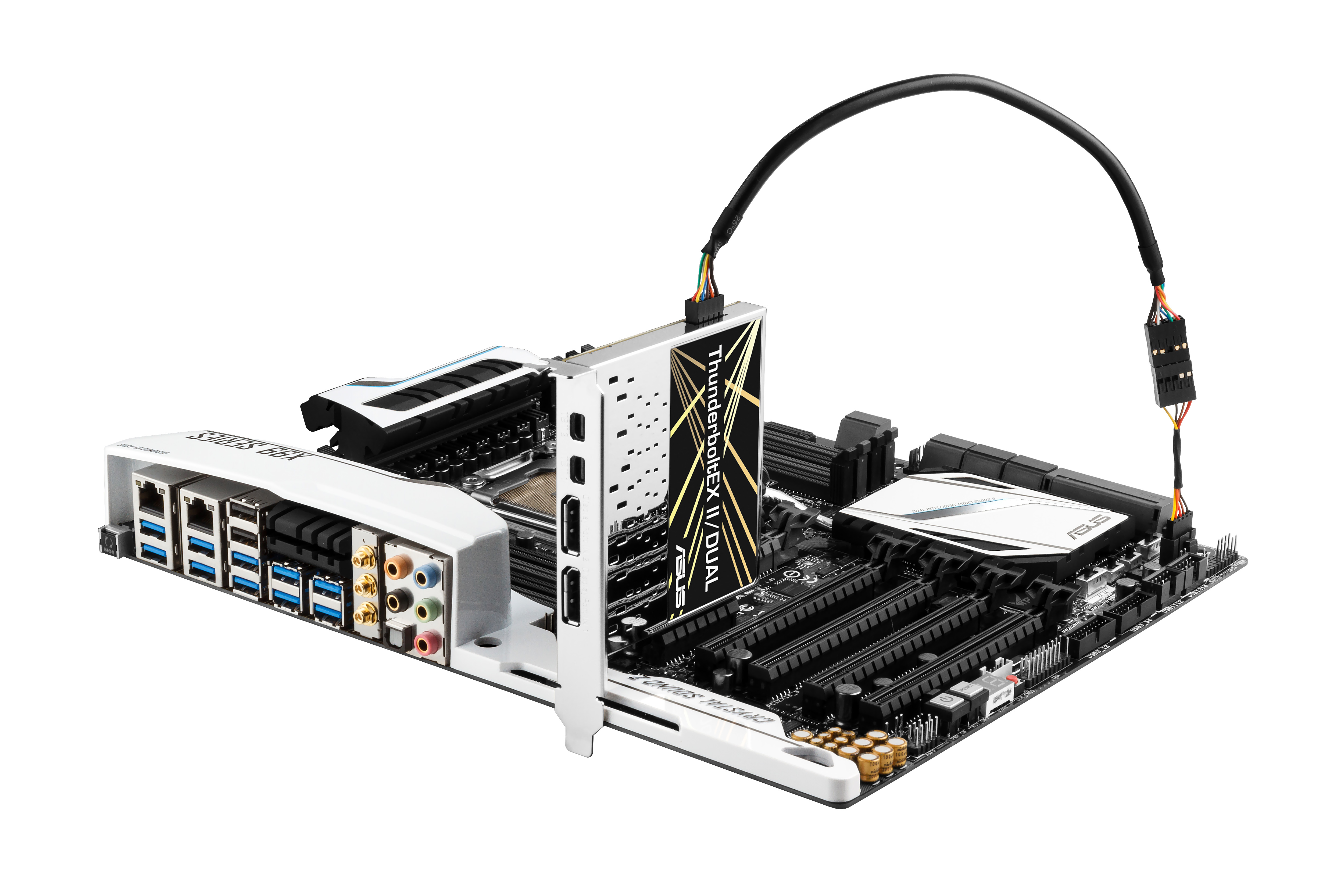
The header below the TPU switch is part of the Thunderbolt functionality, which allows a TB add-in card (sold separately) to be used:
Also on the bottom of the motherboard are two USB 2.0 headers, two USB 3.0 headers, a TPM header, power/reset buttons, a two digit debug, a ClearCMOS button and the fan extension header.

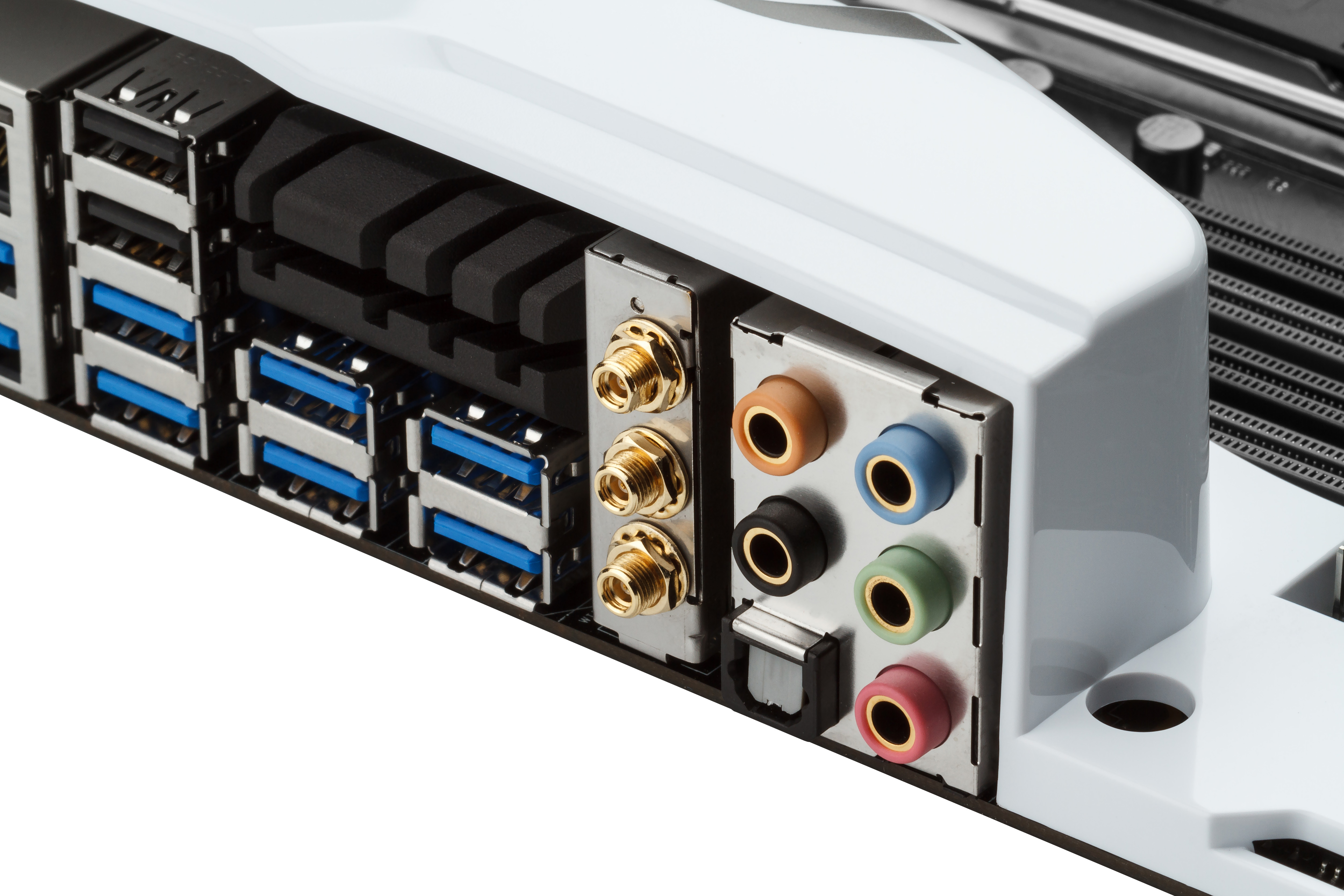
The rear panel does away with PS/2 ports this time around, and the only button here is a BIOS Flashback button. The two network ports are for the Intel I218-V and I211-AT controllers that both support teaming and the ASUS Turbo LAN software. All ten of the USB 3.0 ports are powered by ASMedia controllers (because we have spare chipset lanes), which leaves two USB 2.0 ports, the Broadcom based 3x3 802.11ac card and the gold plated audio jacks.


Board Features
| ASUS X99 Deluxe | |
| Price | US (Newegg) |
| Size | ATX (305x244mm) |
| CPU Interface | LGA2011-3 |
| Chipset | Intel X99 |
| Memory Slots |
Eight DDR4 DIMM slots supporting up to 64 GB Up to Quad Channel, 2133-3200 MHz Non-ECC UDIMMs |
| Video Outputs | None |
| Network Connectivity |
Intel I218-V Intel I211-AT Broadcom 802.11ac 3T3R WiFi |
| Onboard Audio | Realtek ALC1150 with Crystal Sound 2 |
| Expansion Slots |
5 x PCIe 3.0 x16 - 40 PCIe Lane CPU: x16, x16/x16, x16/x16/x8, x8/x8/x16/x8, x8/x8/x8/x8/x8 - 28 PCIe Lane CPU: x16, x16/x8, x8/x8/x8 1 x PCIe 2.0 x4 (Shared with SATAe + USB3_E12) Triple-GPU Config set at x8/x8/x8 due to lane sharing with M.2. Disable M.2 for higher performance |
| Onboard Storage |
6 x SATA 6 Gbps, RAID 0/1/5/10 4 x SATA 6 Gbps 2 x SATA 6 Gbps (ASMedia via SATAe) 1 x SATAe (Intel) 1 x SATAe (ASMedia) 1 x M.2 PCIe 3.0 x4 up to 2280 |
| USB 3.0 |
4 x USB 3.0 via PCH, 2 headers 10 x USB 3.0 via ASMedia, 10 rear ports |
| Onboard |
12 x SATA 6 Gbps 2 x SATAe 1 x Vertical M.2 2 x USB 3.0 Headers 2 x USB 2.0 Headers 1 x TPM 6 x Fan Headers 1 x Fan Extension Header (for 3 more fans_ 1 x Thunderbolt Header EZ XMP Switch SLI/CFX 2/3 Way Switch EPU Switch Two-Stage TPU Switch Thermal Sensor Header DirectKey Header MemOK Button Power/Reset Buttons Clear CMOS Button Two-Digit Debug |
| Power Connectors |
1 x 24-pin ATX 1 x 8-pin CPU |
| Fan Headers |
1 x CPU (4-pin) 1 x CPU-OPT (4-pin) 4 x CHA (4-pin) 3 via fan extension PCB (4-pin) All PWM and DC Controllable |
| IO Panel |
USB BIOS Flashback Button Intel I218-V NIC Intel I211-AT NIC 2 x USB 2.0 10 x USB 3.0 3T3R 802.11ac WiFi Module Audio Jacks |
| Warranty Period | 3 Years |
| Product Page | Link |
Ten USB 3.0 ports on the rear panel of a motherboard is pretty impressive, and we had no issues installing an OS via USB while also having a mouse and keyboard attached. The 3T3R 802.11ac WiFi solution will be something that separates the ASUS from the rest, with small features like EZ XMP and the SLI/CFX switch both being positive additions.
The only port of call that might be a concern is the lack of extra PCIe power, although ASUS is not alone in this issue. If a user was to place a motherboard with the maximum compliment of GPUs and then order up some scalable game or compute, the motherboard might not be able to supply each device with 75W via PCIe and rely on the 6/8-pin power connectors. This suggests that multi-GPU users with 3-4 cards might need a robust power management plan in place.
ASUS X99-Deluxe BIOS
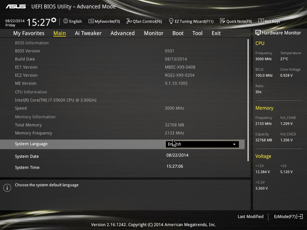
The ASUS BIOS for X99 is going to closely mimic that for Z97, given the close proximity of the launch of the two. The main difference will be catering for the X99 specific features, such as eight DIMMs and the dual AHCI controllers in the chipset. While I would assume that very few users are upgrading from Z97 to X99, those that coming from the 9-series or 8-series motherboards should feel at home. Users coming from the latest X79 builds will notice a slight change towards something more user friendly. First screen up is the EZ mode:
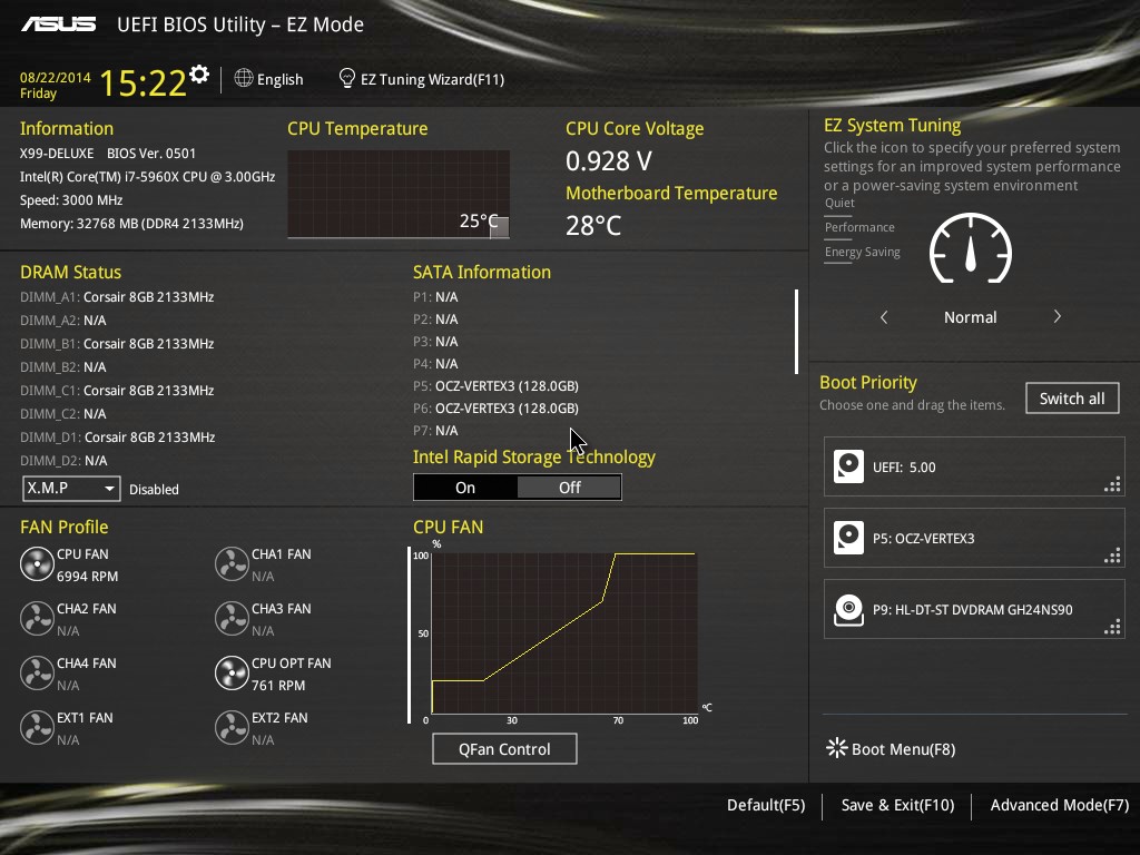
Due to the increased info placed in this first screen, the font size has been reduced slightly, especially when detailing all the DRAM and SATA slots ports that are connected. In this front screen we are told the name of the motherboard, the CPU used, the speed of the CPU, where the DRAM is populated and how much, only with the speed and options for XMP. The CPU and motherboard temperatures are here, with the CPU getting a graph in real time showing how the temperature changes. Voltages and fan speeds are here as well, with a point-to-point graph showing the fan profile of the CPU fan. On the right hand size is an EZ System Tuning icon for performance or energy saving modes as well as a Boot Priority list. On the top of the screen is an option for the EZ Tuning Wizard.
For the fan profiles, selecting QFan Control allows the user to adjust the three point fan gradient:
Each of the fan headers can be controlled by in either DC or PWM mode, with several presets at the bottom and a choice of fan headers on the right. This is the most interactive fan control system within a BIOS to date, however I would suggest a couple of add-ons: a button that sets all the fan profiles at once (otherwise you have to adjust each of them individually), and text showing the current fan speed of the fan selected along with the temperature associated with that fan. In future iterations, perhaps a button to simulate a CPU load (1 core/2 core/4 core) to manually test the fan response might also be considered.
The EZ Tuning Wizard at the top is the new auto tuning mechanism in the BIOS to apply overclocks. As with Z97, this system detects the current outlay, asks what cooling is being used and what the system is for, and then goes back into its internal database to suggest an overclock. This overclock can then be applied automatically:
So here the system is suggesting a 23% overclock, from 3.0 GHz to 3.7 GHz when I selected that I had poor cooling. The reason why the system asks about different types of intended use should come down to single core turbo modes – users interested more in day-to-day responsiveness will want a high single-core turbo, whereas gamers and media editors will want all the cores boosted to the maximum.
Alongside the EZ Mode, the ASUS BIOS offers its characteristic Advanced Mode:
Options here are a little more in-depth and clinical, although ASUS has taken on board suggestions and added both an information section at the bottom and a list of information on the right hand side telling the user what the current state is. Users jumping into X99 from very old systems might be interested in the My Favorites menu, which allows users to select certain options from the BIOS for a custom menu interface:
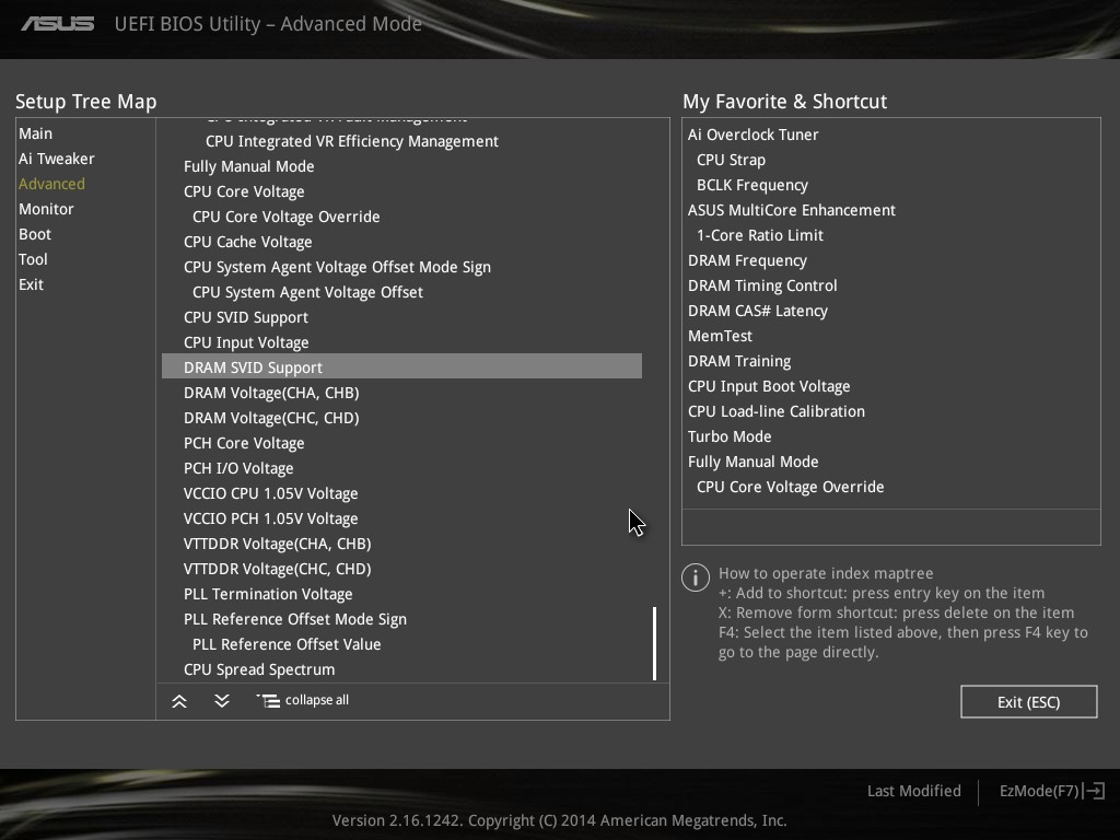
With the Setup Tree Map we can select which options to have in My Favorites, which in my case ends up looking like this:
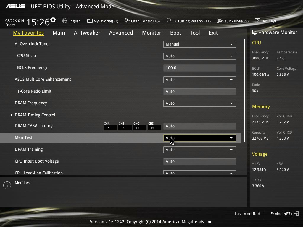
My Favorites is aimed more at overclockers than anything else, allowing these enthusiasts access to frequent settings while bypassing others that are present but might not make a difference in line with the overclocking skill of the individual.
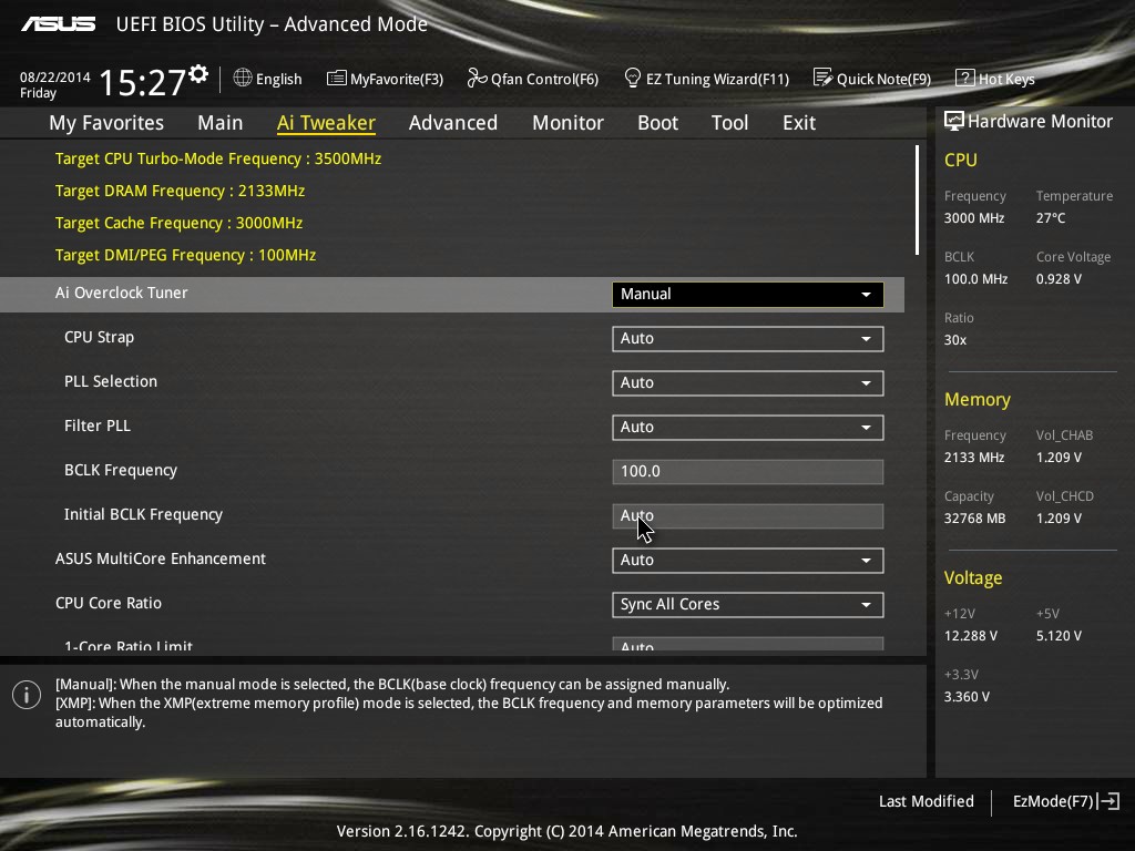
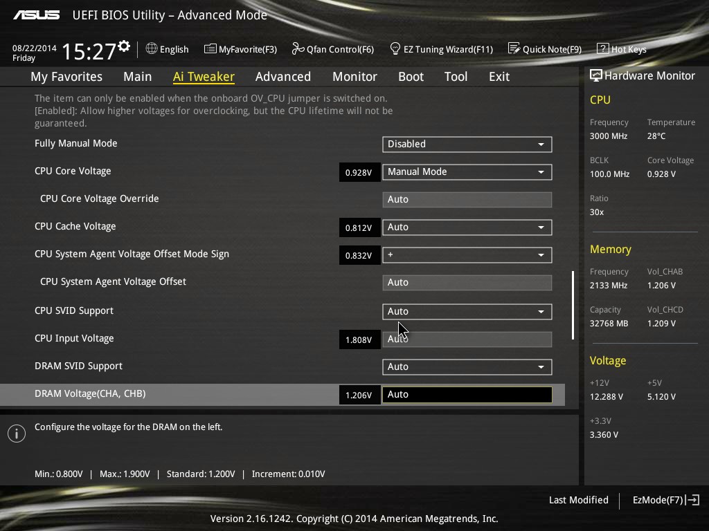
ASUS still keeps the full-fat overclocking menu on hand, giving a full set of options for CPU, DRAM, DIGI+ Power, voltages and power management.
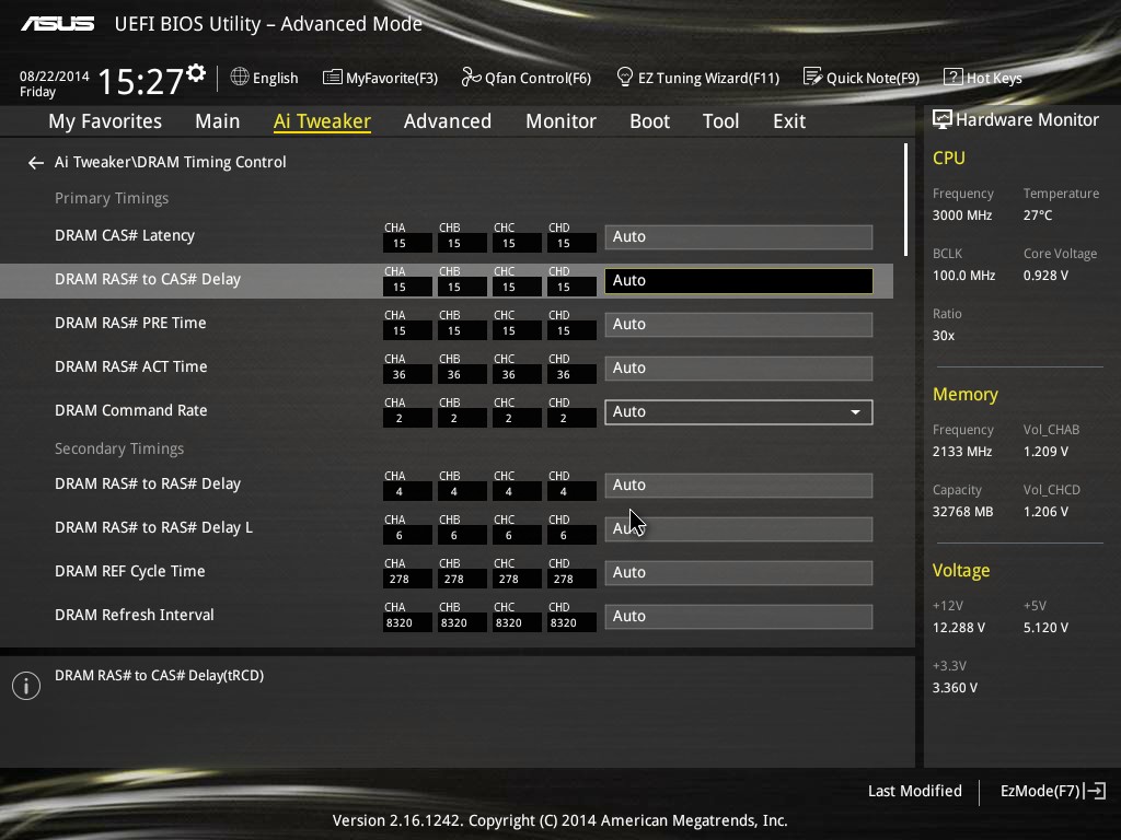
The Advanced Menu gives the usual array of CPU, PCH and Onboard Devices set of configuration menus. A few changes from previous platforms are worth mentioning, such as individual core selection for overclockers:
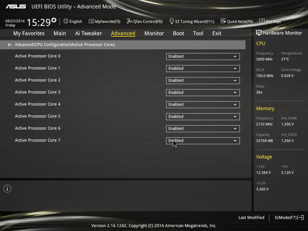
Because not all cores are created equal, the new topology allows users to select specific cores for frequency records.
The onboard devices configuration menu gives the option for adjusting the bandwidth between the controllers onboard that share data paths:
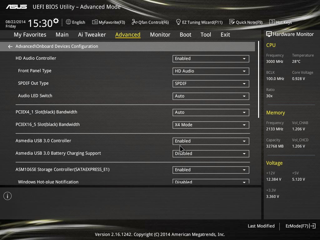
By default the enhanced battery charging of the ASMedia USB 3.0 ports is disabled, and the PCIe_5 slot at the bottom of the motherboard is set to x4 mode.
The Monitor tab gives all the temperature and fan speed data, along with options for the fan headers in a less-interactive but classic implementation:
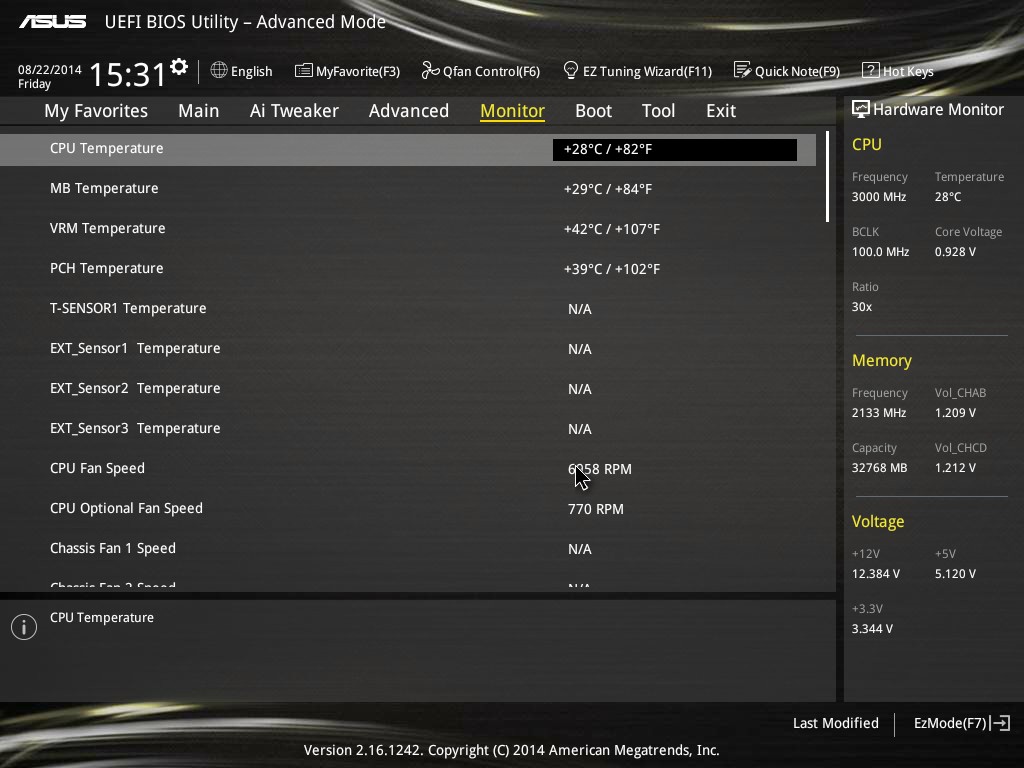
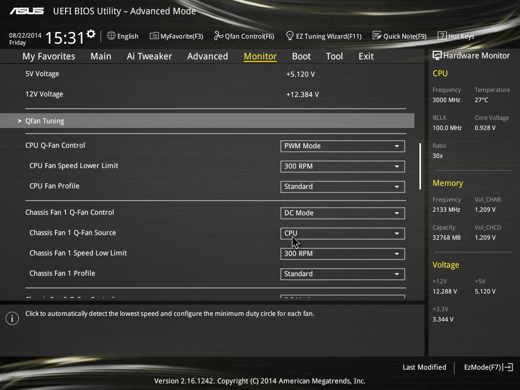
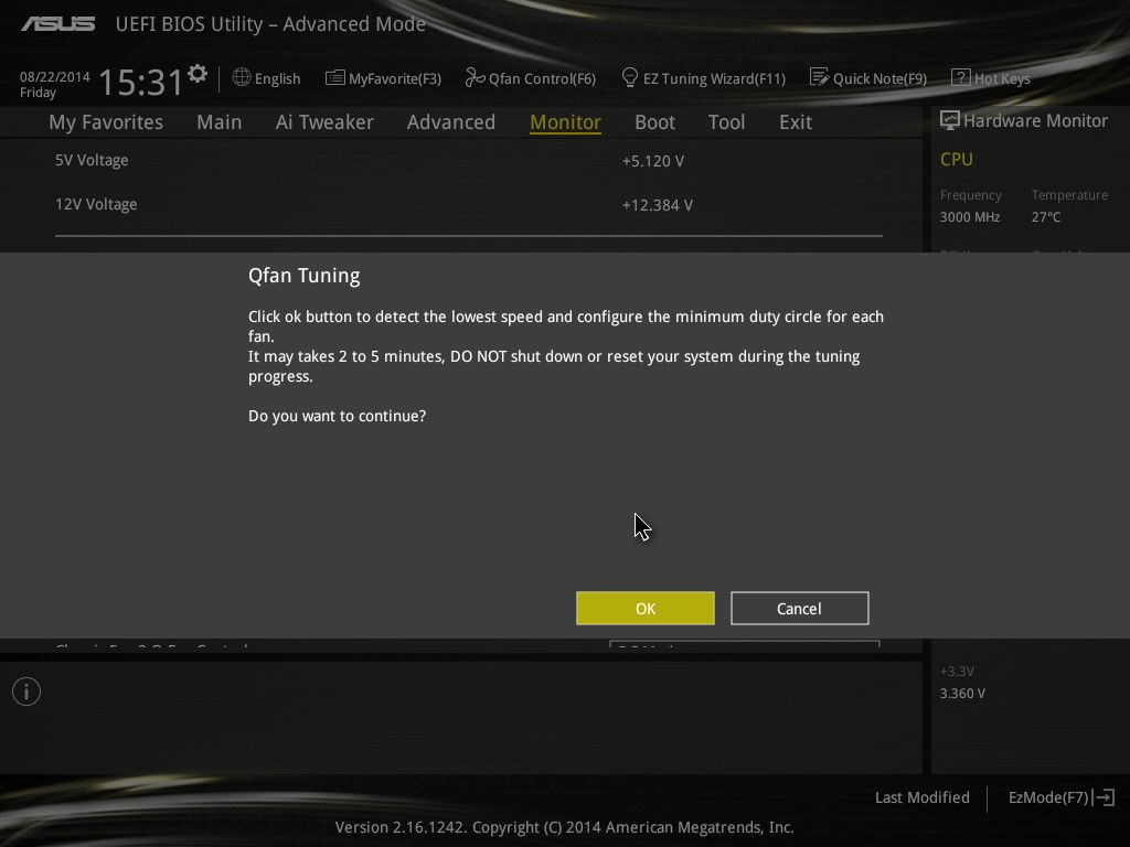
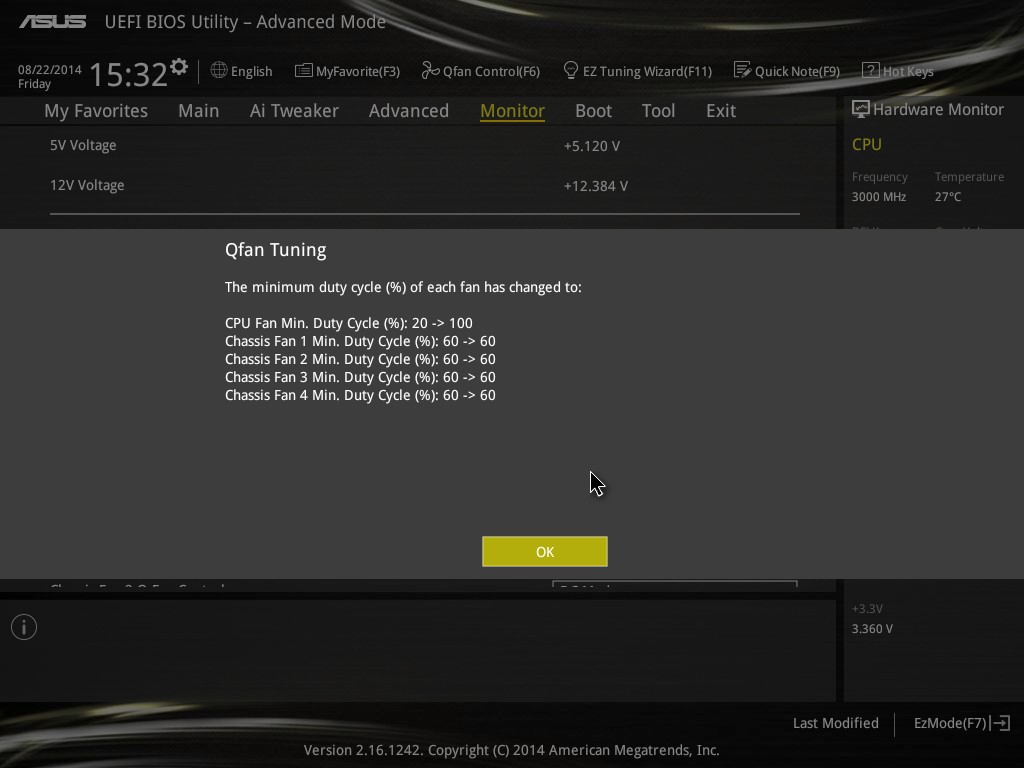
Users can select different modes for each header (PWM or DC), different preset profiles (Standard, Silent, Turbo), adjust which temperature sensor is relevant or adjust a two point gradient manually. The QFan Tuning option provides insight into the workings of each fan by detecting the low-end dead points:
The rest of the BIOS is the standard array of booting options, fast boot options, BIOS flashing tools, OC profiles and SPD information. There is one last feature to mention, the GPU Post screen:
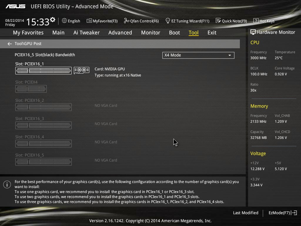
This shows each of the PCIe slots, what is installed and at what speed they are running.
There is one aspect where ASUS is lagging behind the other manufacturers, although GPU Post is part of the way there. ASRock and MSI now implement a ‘Board Explorer’ type function that shows a 2D representation of the motherboard and tells the user what is installed at each point. ASUS should think about this going forward, although it is worth noting that the X99-Deluxe uses 128 Mbit BIOS chips rather than the usual 64 Mbit ICs, suggesting that the BIOS is now getting bigger (and double-sized BIOS chips add cost).


ASUS X99-Deluxe Software
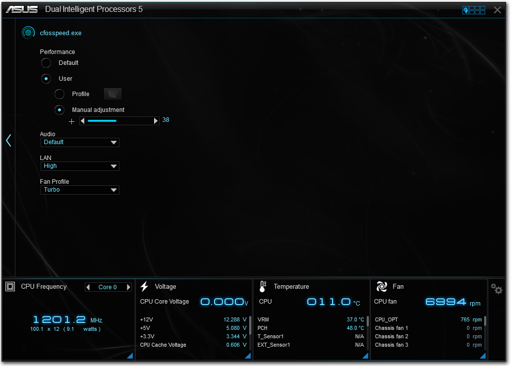
The software stack comes under the AI Suite 3 naming convention, where ASUS’ main play in this area comes from the Dual Intelligent Processors 5 (DIP5) interface. The dual intelligent processors part refers to the onboard EPU and TPU ICs which are ASUS custom designed ICs for monitoring and adjusting both the energy and turbo parts of the system. The 5 at the end of the name refers to both the version and the number of sub-apps within the DIP5 interface.
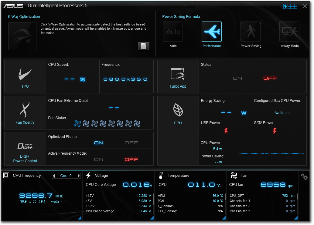
The five sub-apps are the TPU, Fan Xpert, DIGI+ Power Control, EPU and Turbo App. Alongside these is the 5-Way Optimization option that provides a series of settings to help users perform automatic overclocking. This includes options for starting multipliers for stress testing, adjusting the length and type (AVX or other) of stress testing at each stage and goal temperatures. Unfortunately at the time of testing before launch, this feature did not work on our system due to a quirk in our setup although the feature has been fixed for launch.
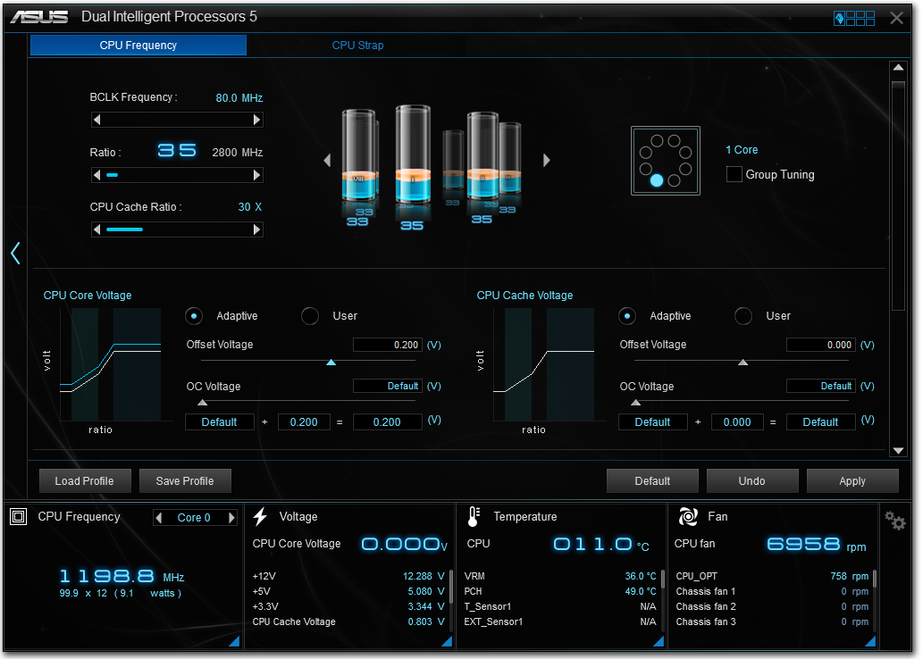
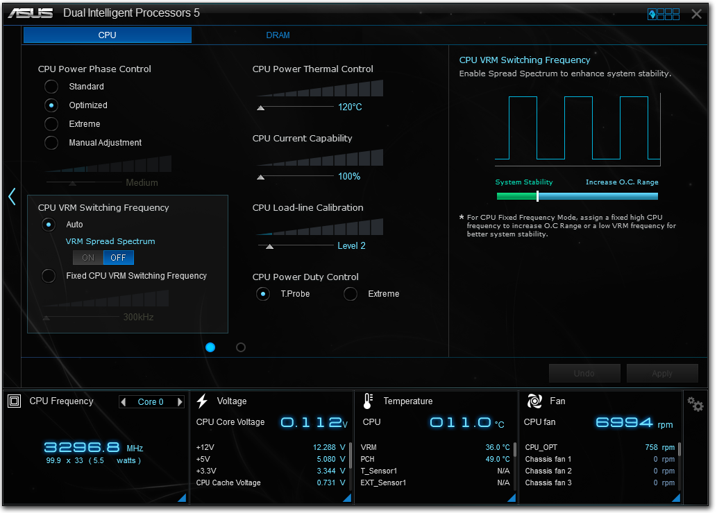
The TPU part of DIP5 offers the CPU overclock settings for ratios, base frequencies, and voltages in terms of offsets and base values. The graphs showing how the voltage adjusts with the CPU ratio are nice touches as they provide direct feedback to the user based on what they are changing.
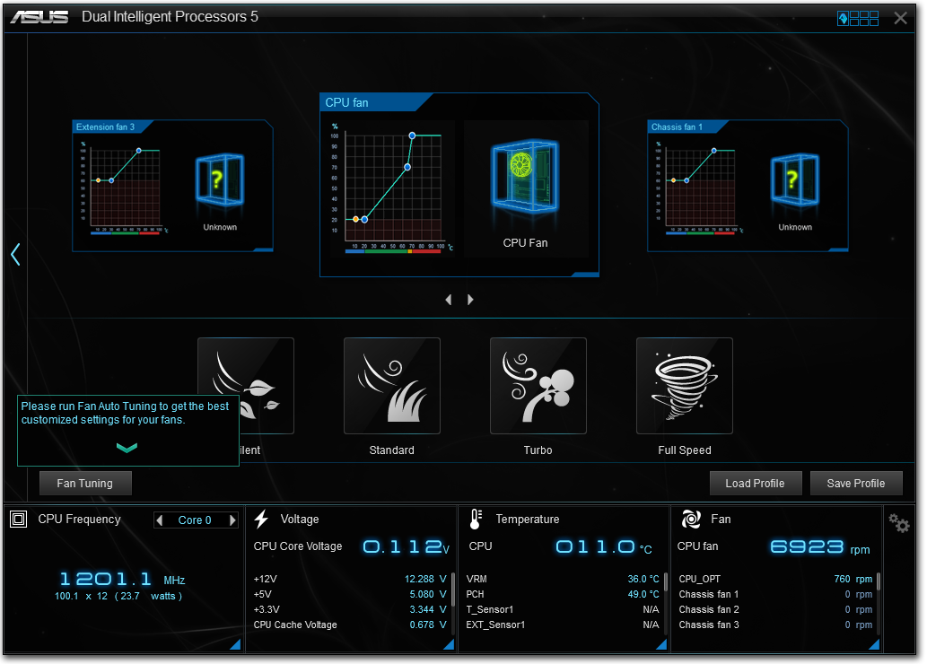
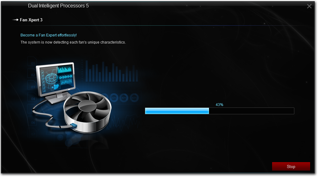
The fan settings allow users to apply a bulk fan mode to all the fans or go in and adjust them manually. The Fan Tuning button on the left provides a way for the system to analyze the characteristics of each fan attached by applying different fan power levels and measuring the RPM.
The digital power controls are for enthusiasts willing to push the system a little further. The automatic overclock options also adjust these settings slightly, giving extra CPU load-line calibration or placing the power phases into extreme performance mode. There are digital power options for both the CPU and the DRAM on hand.
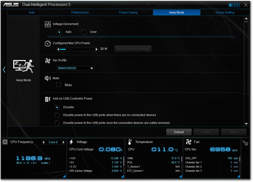
The EPU part of AI Suite allows the user to adjust what is enabled when the system is in a low power mode. This includes a target power consumption for the CPU by reducing clocks and voltage, but also by disabling fast-charging USB ports and turning down CPU fan speeds.
The final part of 5WO is Turbo App, which is the newest addition to the interface. This allows the user to adjust overclocks and settings depending on what software is currently loaded. This means for a linear workload, a user can have the fans turned down but the single thread speed high, or when a game is played we have a full-core overclock with fast fans and LAN priority for the game in question:
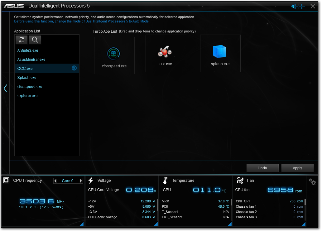
The interface allows each program to be adjusted for importance, so if two software packages are opened and both have a Turbo App profile, the settings of the more important one will take precedence.
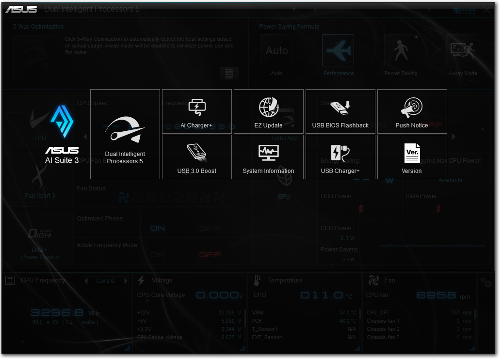
The rest of AI Suite is similar to previous generations on the mainstream platform:
Ai Charger: Gives USB 3.0 charging to BC1.1 compliant devices.
USB 3.0 Boost: Gives a Turbo mode to compatible USB devices.
EZ Update: Online updating software, although still has issues.
USB BIOS Flashback: Arrange a USB for BIOS Flashback.
USB Charger: Allows charging from certain USB ports in sleep, hibernate or shutdown mode.
Push Notice: Synchronize a tablet or smartphone to receive notifications if system parameters (temperature, fan controls) go beyond a specified range.
One element of the software is TurboLAN, which is a reskinned version of cFos that implements software priority over the network:
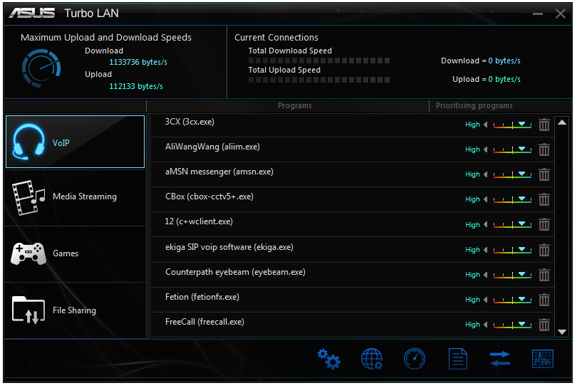
ASUS has preinstalled settings for VoIP, Media, Games or File Sharing, although users can adjust these as required.
One point I would like to request from ASUS is for the Update software to receive an update. As far as it has been part of the ASUS software ecosystem, from the UK it has only ever worked once for me. This is a system that MSI had solved a while ago, with ASRock and GIGABYTE implementing their own systems that work. ASUS is still behind in this regard.


GIGABYTE X99: The New
Similar to ASUS, GIGABYTE comes to X99 with a few new features to tantalize the taste buds of potential users. All new features tend to fall into two categories: improving the underlying product or adding functionality. GIGABYTE is going for a bit of column A and a bit from column B in X99, although we still see stalwarts of the Ultra Durable line as well as upgraded audio.
GIGABYTE’s first major addition to X99 is its use of gold in the connectors. Typically a motherboard manufacturer selects which socket they want from the socket manufacturer (either LOTES or FOXCONN usually) for their motherboards. If the motherboard manufacturer wants something different, then a price is arranged. One of the main components of a socket price above the base is the coating on the pins themselves. Motherboard manufacturers typically use 5-micron gold tipped connections to create a fine line between the copper and the outside world which reduces corrosion and increases the longevity of the device over multiple insertions. For X99, GIGABYTE is using six times the amount of gold in the socket and all PCIe/DRAM connection points:
Technically a thicker coating also affords less resistance for the current to travel through due to the increased diameter, although I question whether this makes a sizable difference on this scale. As long as the user does not accidentally bend a pin in the socket, the main benefit will be for users who are in humid environments and do not use all the PCIe/DRAM slots in their motherboard. I am sure there might be a small benefit to GIGABYTE on returns as well, although I assume the return rate based on corrosion is relatively low.
The next feature is one that benefits anyone who has ever put a PC together. With screwdriver in hand, sometimes placing the motherboard screws in can be a bit of an issue, especially when the screwdriver slips out of the screw head and decides to plunge full force into the delicate components on the motherboard. GIGABYTE has decided to implement an expanded area around each screw hole on the motherboard to make this less of an issue:
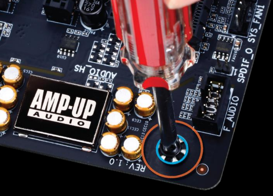
The blue area is where the standard screw mounting hole is, and the orange area is GIGABYTE’s new mounting exclusion zone. These circles are not on the board but the area around each screw hole is definitely free from extra transistors that might get removed by some clumsy hands:
Some of these have printed white text around, but the idea is to at least remove most of the transistors out of the immediate vicinity. I have the unfortunate circumstance of actually being clumsy enough to take a transistor off of one of these motherboards in this review, although for that particular motherboard it did not matter much. If that motherboard had this modification, I probably would not have taken anything off. But there is a lot of if in that statement. Nevertheless, it is an interesting feature to have.
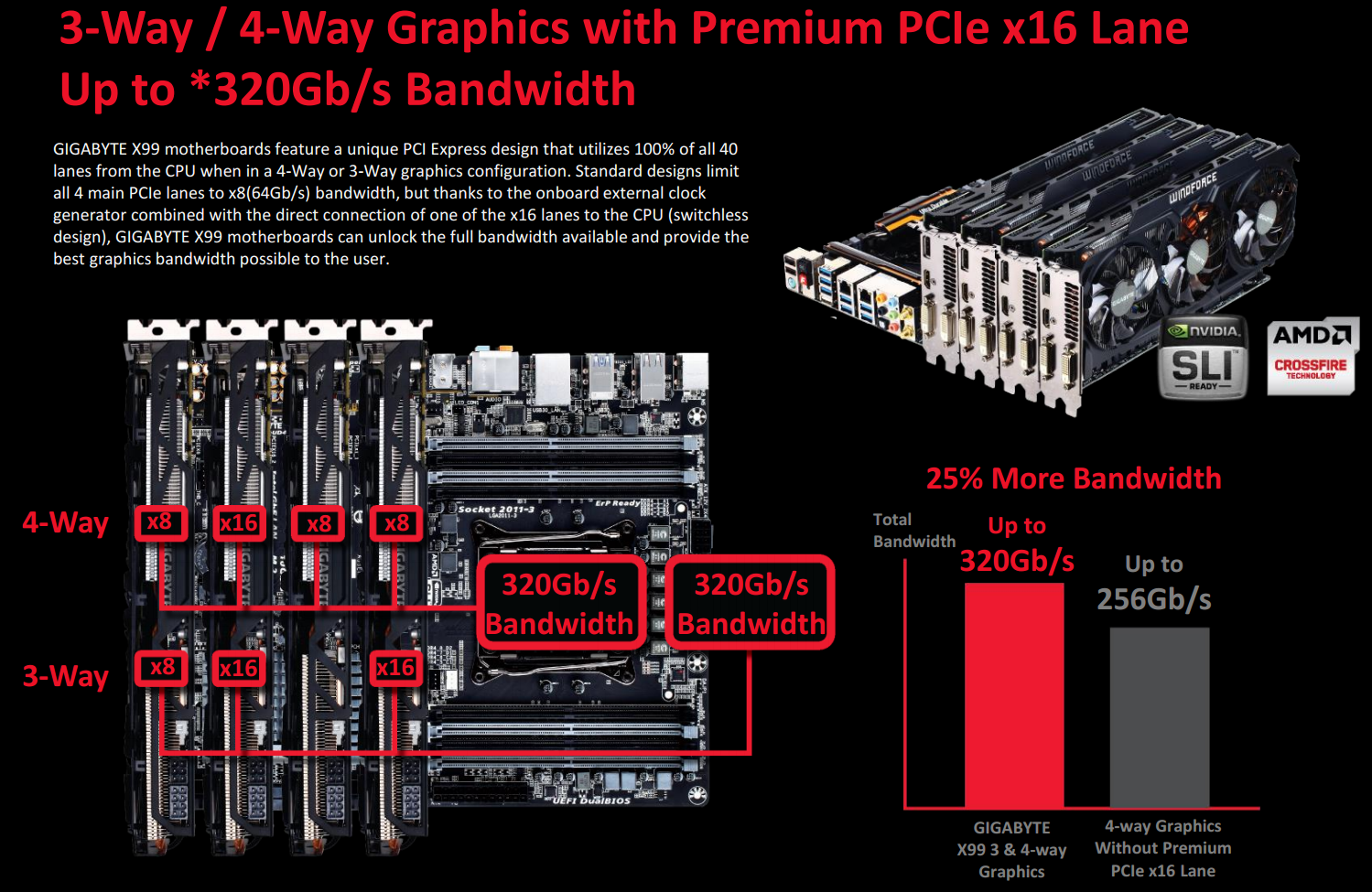
One of the interesting discussions about PCIe bandwidth and X99, aside from the 28 or 40 PCIe lanes debacle depending on which CPU you have, is the one regarding three and four-way GPU setups. Nominally, Intel’s default setting allows x16/x16/x8 for three way, and by using switches this can be expanded to x8/x8/x8/x8 for four-way. But ultimately in this configuration we have lost eight lanes of bandwidth. This is because the CPU essentially has a limited about of PEG lanes it can support with its own clocks, and to get the full x16/x8/x8/x8 scenario, motherboard manufacturers must introduce their own external clock sources. This costs money, so not all manufacturers will do it, however GIGABYTE seems committed to this across its entire product stack:
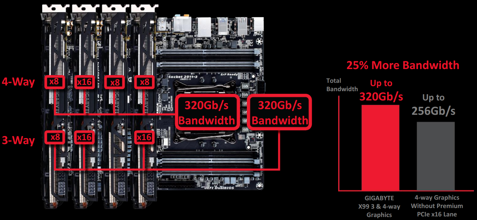
So for example the ASRock motherboard in this review supports only x8/x8/x8/x8, whereas the GIGABYTE X99-UD7 will support x8/x8/x16/x8. There has been some internal discussion because the extra bandwidth might ultimately not make much extra difference to gaming, although it does provide a marketable feature and may be of use to those performing compute based tasks that have bandwidth constraints.
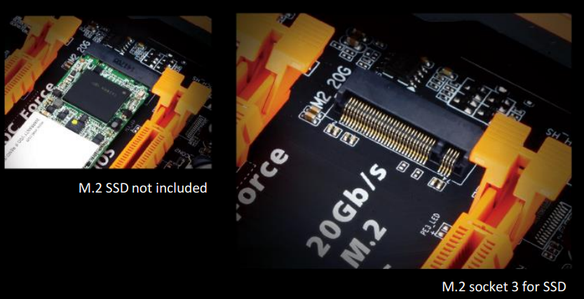
GIGABYTE has also done something slightly different when it comes to PCIe storage, in particular with M.2. M.2 is becoming one of these difficult to predict standards, as it allows PCIe 2.0 x2, PCIe 2.0 x4, PCIe 3.0 x4 and SATA control. This makes it an issue when determining how it is being used on a motherboard. For X99, GIGABYTE is equipping some of its motherboards with two M.2 slots in a stacked configuration, and using one for M.2 based WiFi solutions:
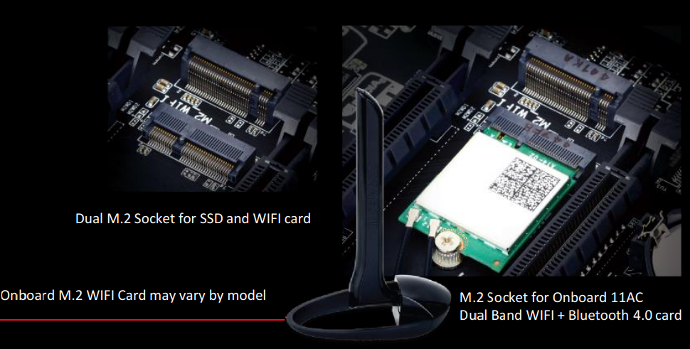
M.2 based WiFi cards have been suggested in the past, although GIGABYTE is going full steam ahead with this implementation, giving connectors to an antenna on the rear panel. This WiFi M.2 slot is at a lower height and has its own screw where needed, with the data based M.2 slot being at a higher height and allowing 2242 to 2280 sized storage devices in a PCIe 2.0 x2 configuration.
For X99 SOC motherboards, GIGABYTE is implementing a ‘Turbo M.2’ socket, with up to 20 Gbps of bandwidth. This means it relies on four PCIe 2.0 lanes from the chipset rather than the CPU, with the thought being that M.2 drives cannot even exploit 20 Gbps at the minute, let alone 32 Gbps. Also, if GIGABYTE did use PCIe 3.0, it would require more configuration alongside the x8/x8/x16/x8 high PCIe bandwidth mode.
GIGABYTE is also introducing a couple of new features for the back panel. One of which we have seen on other motherboards but is new to GIGABYTE – the ability to flash the BIOS without the need for a CPU, DRAM or a GPU to be installed. To go along with the other utilities GIGABYTE provides, this is called Q-Flash Plus.
The feature is actually derived from the Super-IO controller used on board (in this case, an iTE EC 8951E controller), and synchronizes with a single USB port on the rear. With the right named file on the USB stick, it should be a case of plug-in and turn on. An LED will indicate when the process is complete.
The final feature for the rear panel is called ‘Rear Panel LED’, and uses a modified rear panel shield to introduce UV LEDs into the design. When connected with the motherboard, it will cause the back panel to be bathed in a UV glow, making it easier to stick a device in at the dead of night.
Users not too keen on this addition can disconnect the LED and allow the rear panel to go back to normal. The bundled software will allow users to adjust how the rear lights up – either by a constant light, pulsing or responding to the audio coming out of the onboard codec.
GIGABYTE X99-UD7 WiFi Visual Inspection
GIGABYTE announced about ten different SKUs at launch from its Ultra Durable, Gaming and SOC Force lines. With the Ultra Durable units, only certain models will be sold in certain regions. This is going to be true for this X99-UD7, which is aimed more at EMEA (Europe, Middle East, Africa) and APAC (Asia Pacific) than North America which will get the X99-UD5 WiFi instead. The UD5 will be almost identical to the UD7 in feature set, but will have slightly smaller heatsinks and a slightly different bundle, but the underlying design will be the same for both.
In our UD7 WiFi sample, the heatsinks are all connected via heatpipes with a particularly large chipset heatsink to offset a perhaps smaller one for the power delivery. I had no issue installing any graphics cards or cables due to this arrangement, although the positioning of the heatsinks around the socket does limit where GIGABYTE can put the fan headers. The memory slots alternate between grey and black, with the grey ones to be populated first.
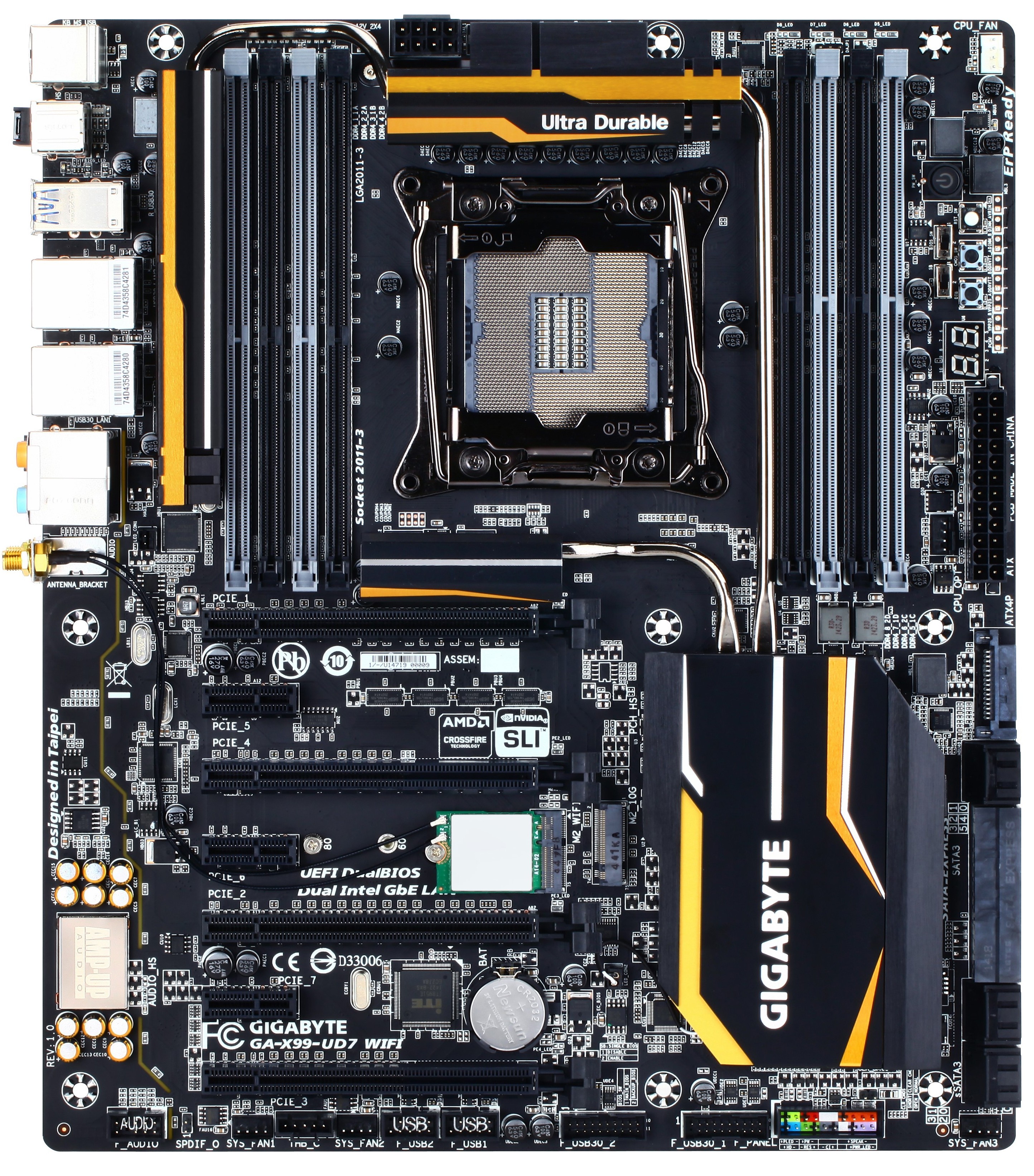
The socket area has only two fan headers within reach due to the heatpipe arrangement – one four pin CPU header in white in the top right of the board, and a 4-pin CPU OPT header next to the 24-pin ATX connector. The other three headers are at the bottom of the board, one on the right and the other two just left of center. These are also 4-pin and labeled as system fans. Having only five fan headers seems relatively few for a high end motherboard.
The power delivery arrangement means that a single CPU 12V 8-pin connector is preset at the top of the board, and most of the extra overclocking options are on the right hand side. Here we get a power button, a reset button, a BIOS switch, a CMOS reset, a switch to enable DualBIOS, and a button to reboot straight into the BIOS.

Underneath these are voltage read points for overclockers, and to the left is a two digit debug display for diagnosing POST problems.
Further down the right hand side is a SATA power connector to add in additional power to the PCIe slots. Out of all the different ways to supply PCIe power, this location is the best: either in the form of a SATA connector or a 6-pin PCIe connector where possible. The 10 SATA ports are split into six RAID capable at the top (listed as SATA) and four more non-RAID at the bottom (listed as sSATA). GIGABYTE is implementing both SATA Express and M.2 on the UD7, meaning that bandwidth is switched between which one is in operation when the machine is turned on.
The bottom of the motherboard features three 4-pin fan headers, a Thunderbolt header, two USB 2.0 headers, two USB 3.0 headers, the front panel audio header and the front panel control header. Both of the USB 3.0 headers are powered by the chipset, with another two from the chipset on the back panel split into eight via dual Renesas USB 3.0 hubs.
For the PCIe arrangement, GIGABYTE has labeled them in a very odd manner. The top port is called PCIe_1, but then follows PCIe_5, PCIe_4 and PCIe_6. PCIe_2 is the third full length slot, with PCIe_7 and PCIe_3 at the bottom.
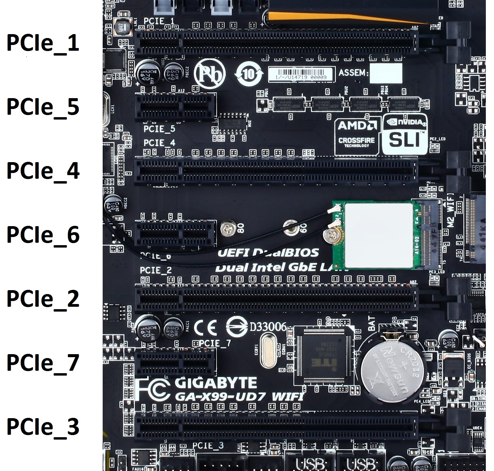
Why this arrangement? So users will fill up the PCIe slots starting with number 1, followed by 2, 3 then 4. This is an odd way of arranging things – a complete contra-strategy to the rest of the motherboard industry who count from the top down. If GIGABYTE plans to make this sort of arrangement permanent, they need a light-up idea like ASUS. If not, then change it back otherwise some users will get headaches.
The following occurs with PCIe 1/4/2/3 full length slots (so from the top of the board down):
CPU with 40 PCIe lanes: x16/-/-/-, x16/-/x16/-, x16/-/x16/x8, x8/x8/x16/x8
CPU with 28 PCIe lanes: x16/-/-/x4, x16/-/x8/x4, x8/x8/x8/x4
Each of these PCIe slots also have the 30-micron gold used by GIGABYTE in its X99 range.
The M.2 arrangement in the middle of the PCIe slots is a little different to the other motherboards in this roundup. Here we have two M.2 slots, but one is being used for the WiFi. The Intel AC7260 was used in our sample, and this uses one PCIe 2.0 lane from the chipset to operate with the antenna reaching around to the rear panel. Our WiFi solution had a plastic tag stuck to the motherboard for the antenna wires to go through, ensuring they stayed close to the PCB and not get in the way of any PCIe devices. The other M.2 slot is a normal PCIe 2.0 x2 solution, capable of either x1 or x2 mode, sharing bandwidth with the SATA Express slot.
The audio next to the PCIe slots is GIGABYTE’s enhanced Realtek ALC1150 audio package dubbed ‘AMP-UP Audio’. Other features such as Op-Amp adjustment and gain switches are not on this model.
The rear of the motherboard, when the shield is used, is fitted with additional UV lighting to add to the aesthetic. There is a 2-pin cable in the shield which fits into a header just behind the two WiFi antenna on the main motherboard PCB.

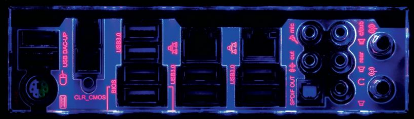
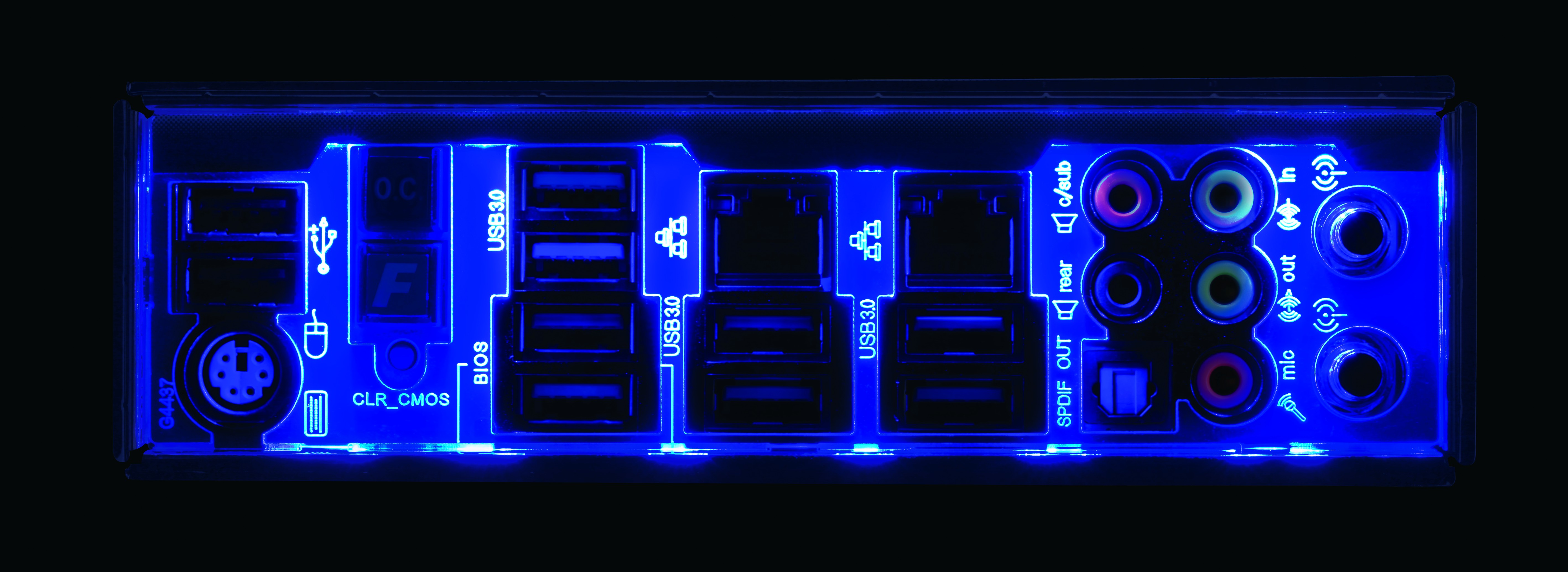
This image is easier to dissect: we get a combination PS/2 port, two USB 2.0 ports, an OC Button, a Fast Boot button, a ClearCMOS button, eight USB 3.0 ports (from Renesas Hubs connected to chipset USB ports), the white Q-Flash port, two Intel network ports (I210-AT and I218-V), audio jacks and dual WiFi antenna.


GIGABYTE X99-UD7 WiFi Board Features
| GIGABYTE X99-UD7 WiFi | |
| Price | US (Newegg) |
| Size | ATX |
| CPU Interface | LGA2011-3 |
| Chipset | Intel X99 |
| Memory Slots |
Eight DDR4 DIMM slots supporting up to 64 GB Up to Quad Channel, 2133-3000 MHz Support for RDIMM 1Rx8 Non-ECC |
| Video Outputs | None |
| Network Connectivity |
Intel I210-AT Intel I218-V Intel 7260 AC 2T2R via M.2 |
| Onboard Audio | Realtek ALC1150 via AMP-Up Audio |
| Expansion Slots |
4 x PCIe 3.0 x16 - 40 PCIe: x16, x16/-/x16, x16/-/x16/x8, x8/x8/x16/x8 - 28 PCIe: x16/-/-/x4, x16/-/x8/x4, x8/x8/x8/x4 3 x PCIe 2.0 x1 |
| Onboard Storage |
6 x SATA 6 Gbps, RAID 0/1/5/10 4 x S_SATA 6 Gbps, no RAID 1 x SATA Express 1 x M.2 x2, support for 2242 to 2280 1 x M.2 x1 (WiFi included) |
| USB 3.0 |
4 x USB 3.0 via PCH as two headers 8 x USB 3.0 via Renesas Hubs as eight rear ports |
| Onboard |
10 x SATA 6 Gbps 1 x SATA Express 1 x M.2 x2 5 x Fan Headers 2 x USB 3.0 Headers 2 x USB 2.0 Headers Power/Reset Buttons Two Digit Debug LED Clear CMOS Button Direct to BIOS Button BIOS Switches Voltage Measurement Points Front Panel Header Front Audio Header |
| Power Connectors |
1 x 24-pin ATX 1 x 8-pin CPU 1 x SATA for PCIe |
| Fan Headers |
1 x CPU (4-pin) 1 x CPU-OPT (4-pin) 3 x SYS (4-pin) |
| IO Panel |
1 x Combination PS/2 Port 2 x USB 2.0 Ports 8 x USB 3.0 Ports (via Renesas Hub) - White USB for Q-Flash 2 x Intel Network Ports (I210-AT and I218-V) OC Button Fast Boot Button ClearCMOS Button Audio Jacks 2 x WiFi Antenna Points |
| Warranty Period | 3 Years |
| Product Page | Link |
GIGABYTE is focusing on four-way PCIe orientations across its whole range, whereas most other manufacturers are doing some for three-way and others like this. Five fan headers seems a small amount, but it is interesting to see M.2 used for WiFi in this fashion. I can only assume that GIGABYTE has managed to purchase these in bulk such that the price is similar to a mini-PCIe design – the M.2 design is at least smaller. What GIGABYTE has to consider now is that ASUS is implementing 3T3R, and if a ‘UD9’ type of motherboard at $400 might be worth this sort of adjustment.
GIGABYTE X99-UD7 WiFi BIOS
In the past couple of generations, GIGABYTE’s BIOS setup has been in a difficult place. Everyone is now part of the graphical BIOS era, but migrating from a series of regular menus to something more interactive is a hard part. At some point in the journey, aesthetics and visuals have to be addressed. When the visuals are focused on first, then the system is negatively impacted by not bringing anything new to the table. When interactivity is focused on at the expense of any element of aesthetic improvement, this means that the user experience is terrible. Every motherboard manufacturer is churning through this slurry of what a graphical, interactive BIOS is meant to be like, and GIGABYTE’s journey has been tougher than most.
Initially it started with ‘3D BIOS’, which was a visual representation of the motherboard that was not executed with users in mind. Within the past 18 months GIGABYTE ditched the 3D BIOS in favor of a HD mode. This had its own initial issues – the text was not calibrated to work within the confines of the various boxes to which it was assigned, and the orange/black/grey color scheme was not easy on the eyes, especially for anyone with slight colorblindness. HD Mode itself is a full 1080p high definition implementation, allowing more information on the screen at once, although the menu system was almost a carbon copy of what was found in the classic mode. Interactivity is still minimal, with almost everything being in a text menu or a drop down.
For X99, several things have changed for the BIOS. The classic mode gets a facelift and moves to a cleaner but blockier interface with a good contrast between text and background. In the HD mode, the text now all fits in the boxes and there is some improvement to adjust the visual differentiation between background and text, but more could still be done. Interactivity is still quite minimal, with classic and HD mode featuring many of the same options slightly rearranged.
The first entry screen is the Startup Guide which is the main recipient of text adjustment, but we also get a few more options to fill up this 3x3 grid. It might make sense that in the future GIGABYTE implements a 5x5 grid with various quick access to options (!).
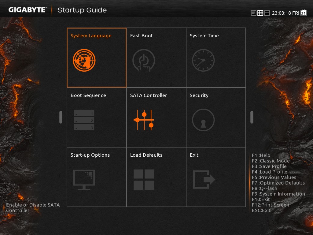
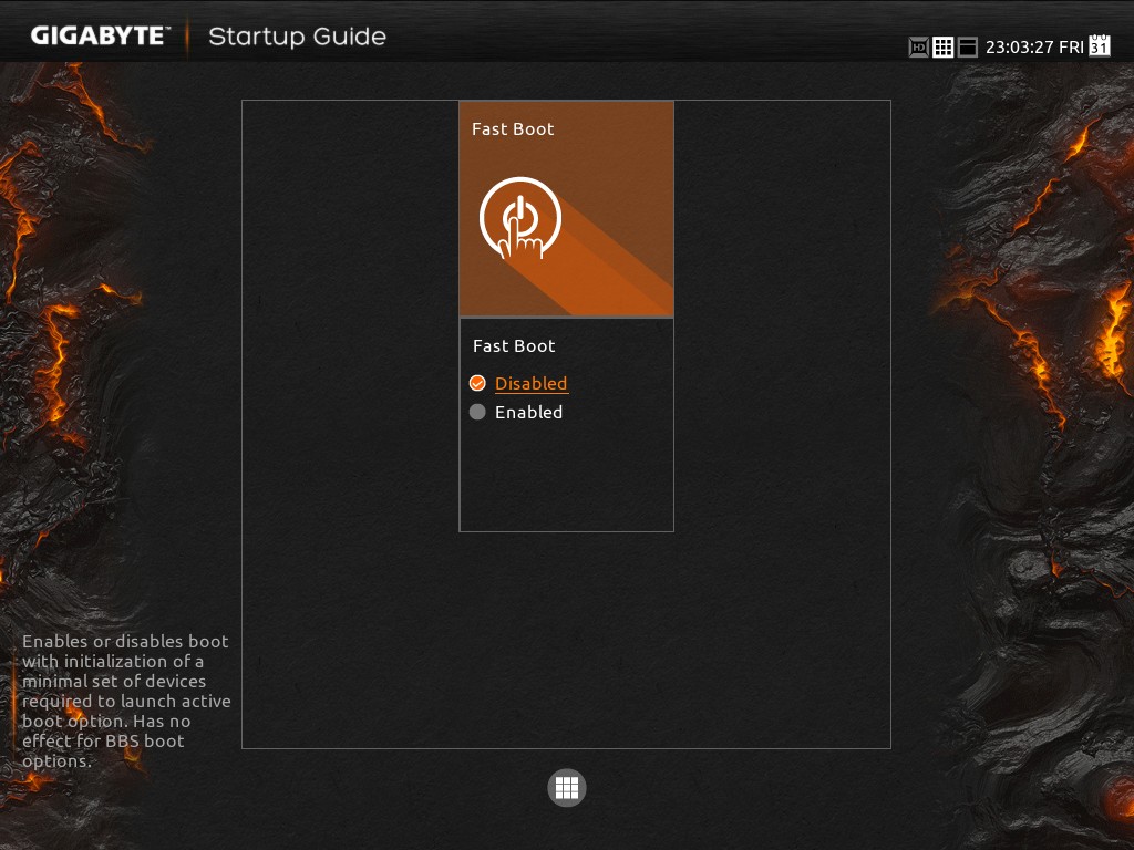
Most of these are self-explanatory. Fast boot gives options related to Windows 8 such that devices are not initialized until later in the OS boot process, speeding up overall POST time:
The SATA controller option text now all fits nicely into each of its boxes, although due to the dual AHCI controller nature of the chipset and only six SATA ports having access to RAID, it does not help the user much if the drives are plugged in the wrong ports:
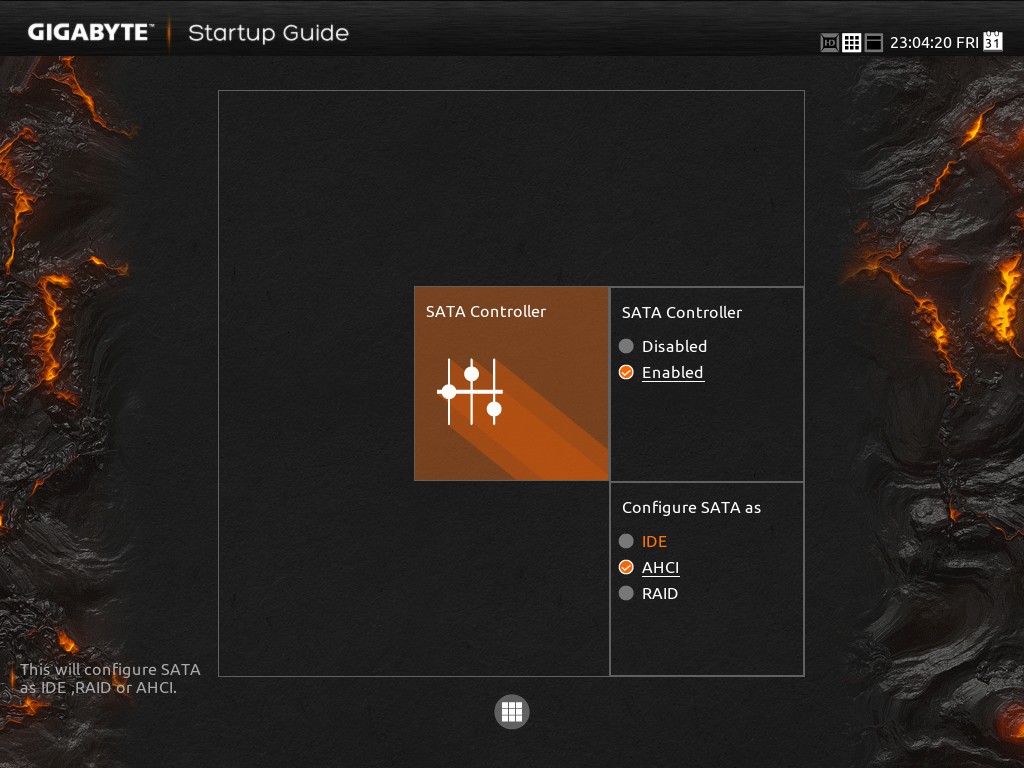
Ideally we would see an explanation giving SATA versus sSATA ports on the motherboard used, and what drives are installed where.
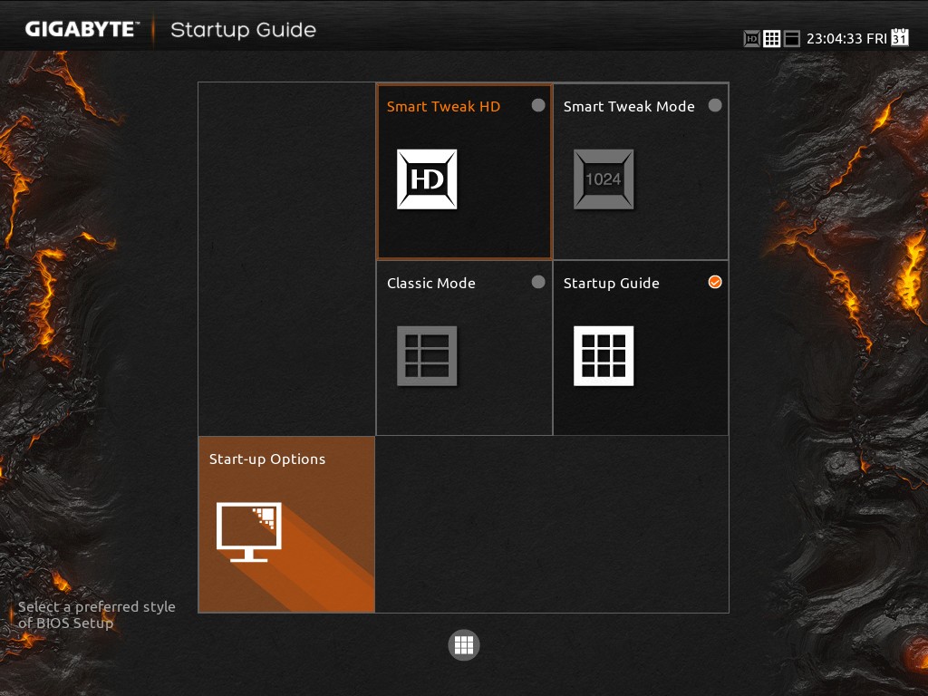
The Startup Options allows the user to boot into any of the four modes available. The HD mode does offer a smaller sized version with less information if the monitor is not capable of 1920x1080.
Despite a nice start guide for users, it would help if the initial screen detailed the system, perhaps in the top left. We want to see the name of the motherboard, the BIOS used, the CPU installed, the DRAM installed and frequencies where possible. That way any user trying to debug the system without having access to the insides will be able to see immediately what is at hand.
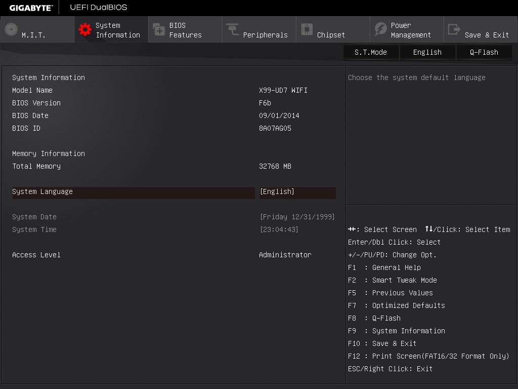
The standard classic mode gets an update from the blue interface to a sleeker grey and white menu system. The layout is pretty much the same as before, along with the information provided. For example, the entry point offers the model name of the motherboard and the BIOS version, but no mention of the CPU installed.
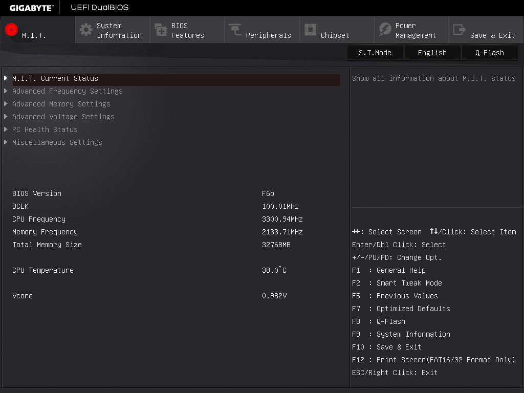
Even moving to the Motherboard Intelligent Tweaker menu (MIT) does not display this information, although we do get the VCore, CPU temperature and various frequencies on hand.
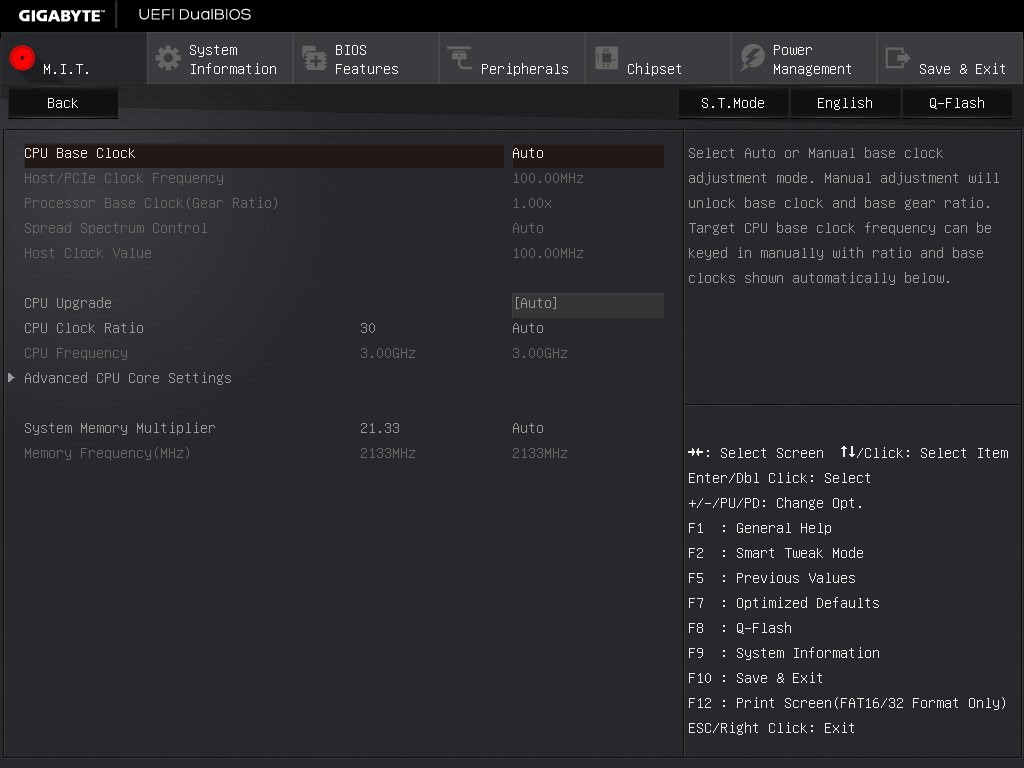
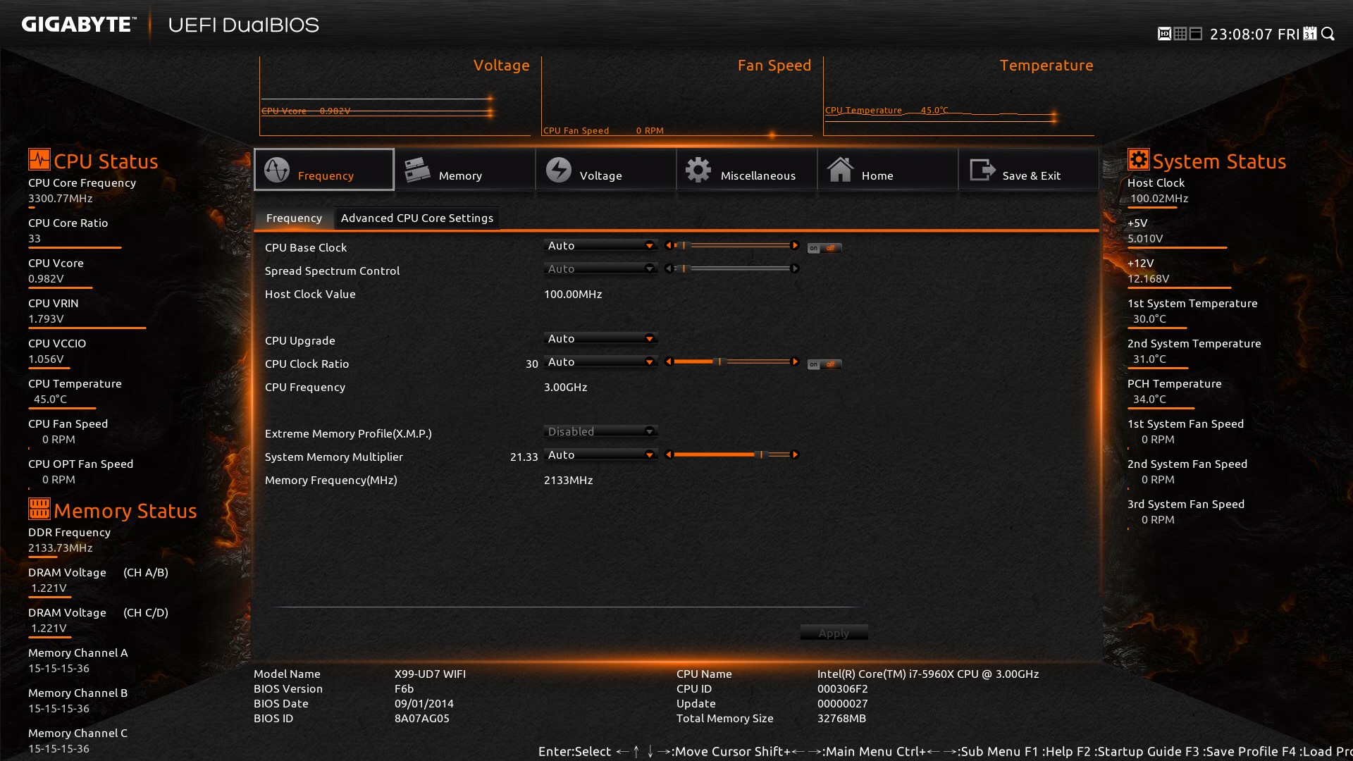
The overclocking options in the GIGABYTE BIOS are only for manual overclocking, and split into several sub-menus coming from the MIT tab. The Frequency menu allows the user to adjust the CPU and DRAM:
In order to adjust the per-core ratios or the Uncore and C-states, the CPU Core Settings menu is provided:

Note that there are no voltage options in either of these menus. GIGABYTE’s reasoning is that the voltage options are solely for the voltage menu, but I differ. Motherboard manufacturers can place the same option in multiple menus, but often choose not to for reasons of layout or space or to avoid confusion. I do not see that as an issue – if anything, I believe it would enhance the experience especially for an enthusiast wanting to adjust these settings. So while the voltage settings are not duplicated, the DRAM frequency strap is – we see it here in the Advanced Frequency menu and also in the Advanced Memory menu:

It makes no sense to duplicate this option and not others.
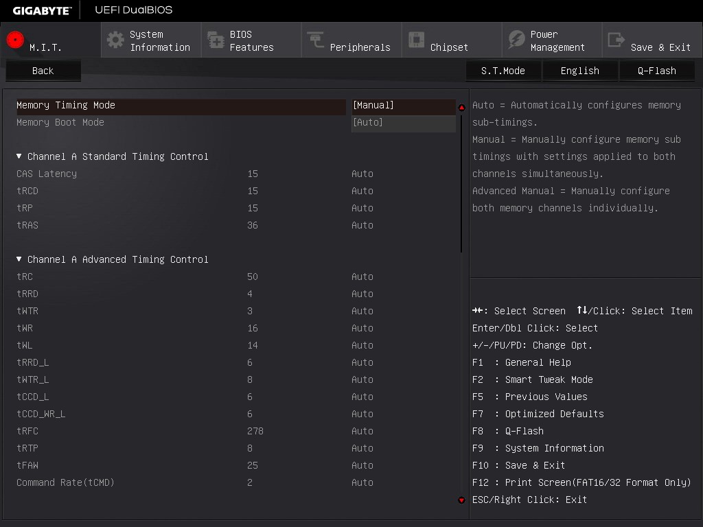
In order to adjust sub-timings for the memory, as with previous GIGABYTE motherboards, the memory timing mode must be changed to ‘Manual’ to set a rule for all modules or ‘Advanced Manual’ to set per-module timings.
GIGABYTE has adjusted how the BIOS communicates what each option means to the user in the top right of the screen. I remember one of my contacts at GIGABYTE was writing the initial drafts for these info texts earlier in the year, and remarking that it was no small feat especially after several iterations and then sending it to the translators for other languages and making sure no subtleties were lost.
The Advanced Voltage Setting menu is split into several sub-options.

The Power Settings menu is for voltage protection options, current protection and switch rate adjustment. The most important option though is the Load Line Calibration for the FIVR:
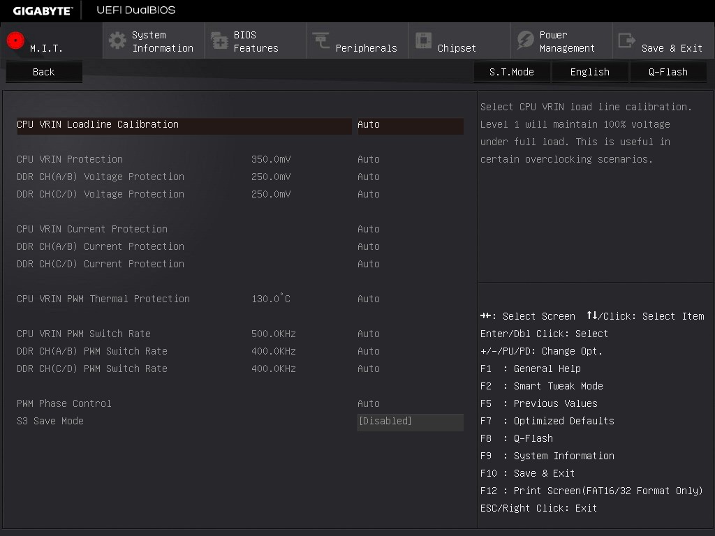
As mentioned in the help text, the top setting will maintain 100% voltage at load to combat the regular voltage drop across the processor as the workload varies.
The Core Voltage menu is where the meat of the CPU voltage options are:
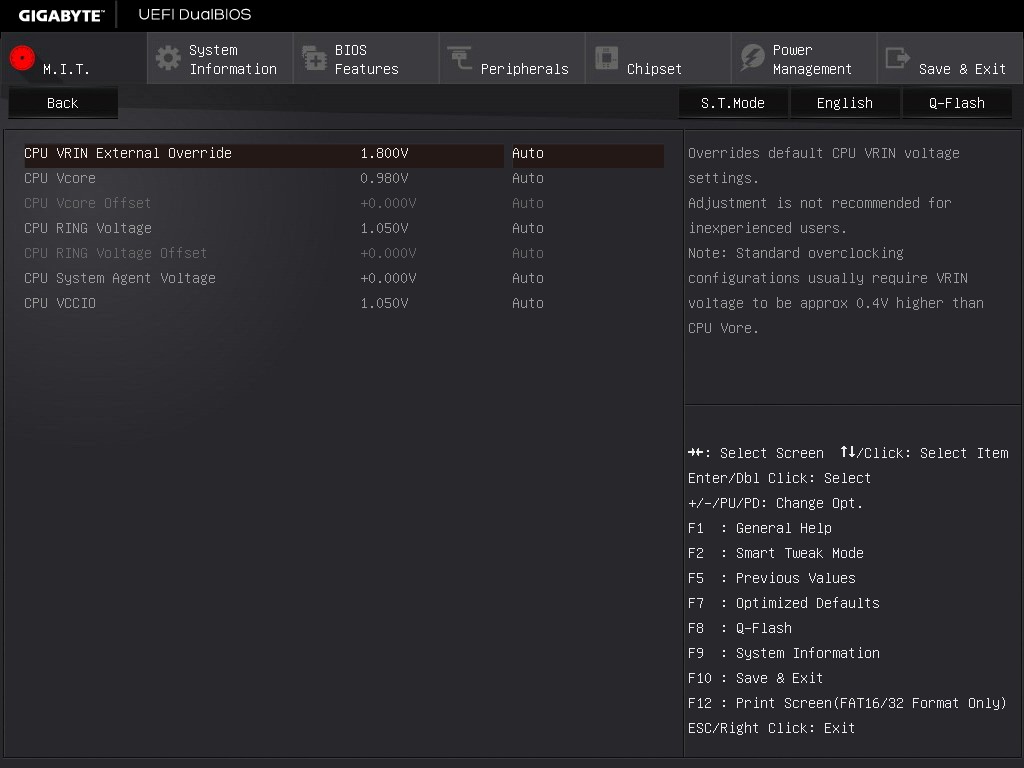
Adjustments to the VRIN (FIVR), VCore and Cache voltages are here, with only absolute values allowed. Other manufacturers offer both offset and absolute choices for these values although I find offset values more applicable for automatic overclocking options.
The fan controls in the classic mode are in the PC Health option from the MIT tab.
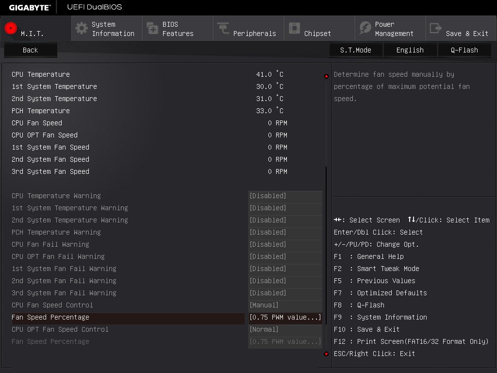
While the system has four temperature sensors and five fan headers, the level of fan speed options in the BIOS is very basic.
For anyone not used to a value describing how one variable adjusts with another, the options here might make no sense. The power applied to a fan is a ‘PWM’ number from zero to 255. GIGABYTE’s options allow you to adjust that value based on the temperature, in terms of ‘PWM per ºC’. So a CPU temperature of 50ºC at 2 PWM per ºC will give a value of 100, which means that 100/255 = 39.2% of the full power of the fan is used. To confuse the matter even more, a fan does not respond linearly to power increases, and GIGABYTE does not mention of this value has a base number.
Other manufacturers have the fan controls in the BIOS at a state where they are a lot easier to follow, and GIGABYTE has fallen behind in adapting their controls to a more interactive interface that is easier to understand.
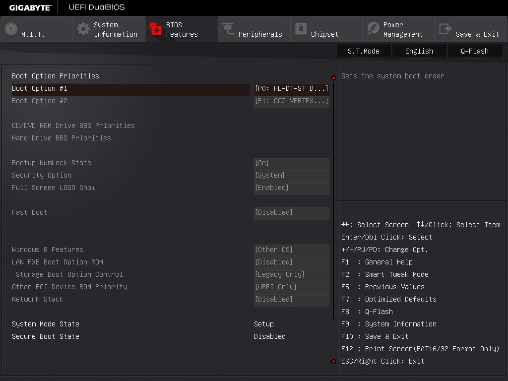
The BIOS Features tab relates to the boot order and fast boot options:
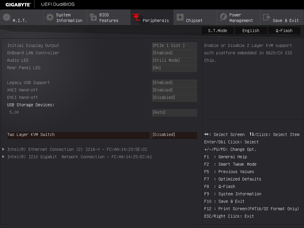
The Peripherals tab involves LED options, enabling onboard controllers and an interesting option relating to KVM switches:
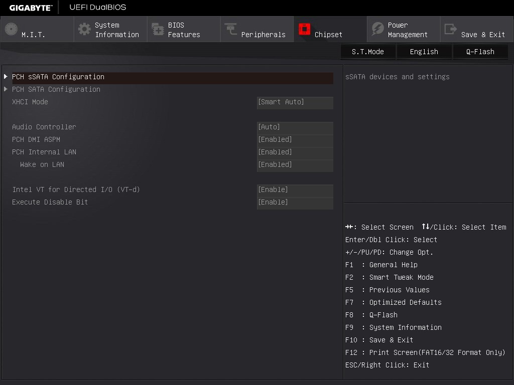
The Chipset tab is for SATA adjustments, with GIGABYTE offering different menus for the sSATA (non-RAID) and SATA (RAID) AHCI controllers:
The rest of the classic BIOS allows for power management and BIOS flashing, with the Save and Exit menu giving boot override possibilities.
The full HD mode uses a similar sort of option arrangement in the middle of the screen with as much information as you can pack into the surrounding edges. Most BIOSes need something like this around the edge to tell the user about the system, although I might suggest that having bars underneath values such as ‘CPU VRIN’ are ultimately not necessary and could be cleaned up. The ideal BIOS is one that displays everything succinctly without wasted space but still visually effective. For example, perhaps graphing the voltage change over time in the BIOS is not particularly helpful.


GIGABYTE X99-UD7 WiFi Software
Similarly to the BIOS, the software has been upgraded over the past 18 months. Easy Tune 6 is out, and the new interface is a sleek color-on-black design. This allows GIGABYTE to alter the color palette depending on what motherboard is being used – blue for Ultra Durable, orange for SOC and yellow/green for gaming. So despite the accents on our UD7 being yellow/orange, the software has a blue-on-black style, but this can be adjusted in the preferences.
The base menu system is called APP Center which shows the various ‘apps’ in a scrollable window. The Live Update element on the bar is fixed, while the rest are sorted in alphabetical order. I hope that in future updates we are able to fix a preferred option at the top as well, given that I primarily use EasyTune for overclocking or System Information Viewer for fan controls.
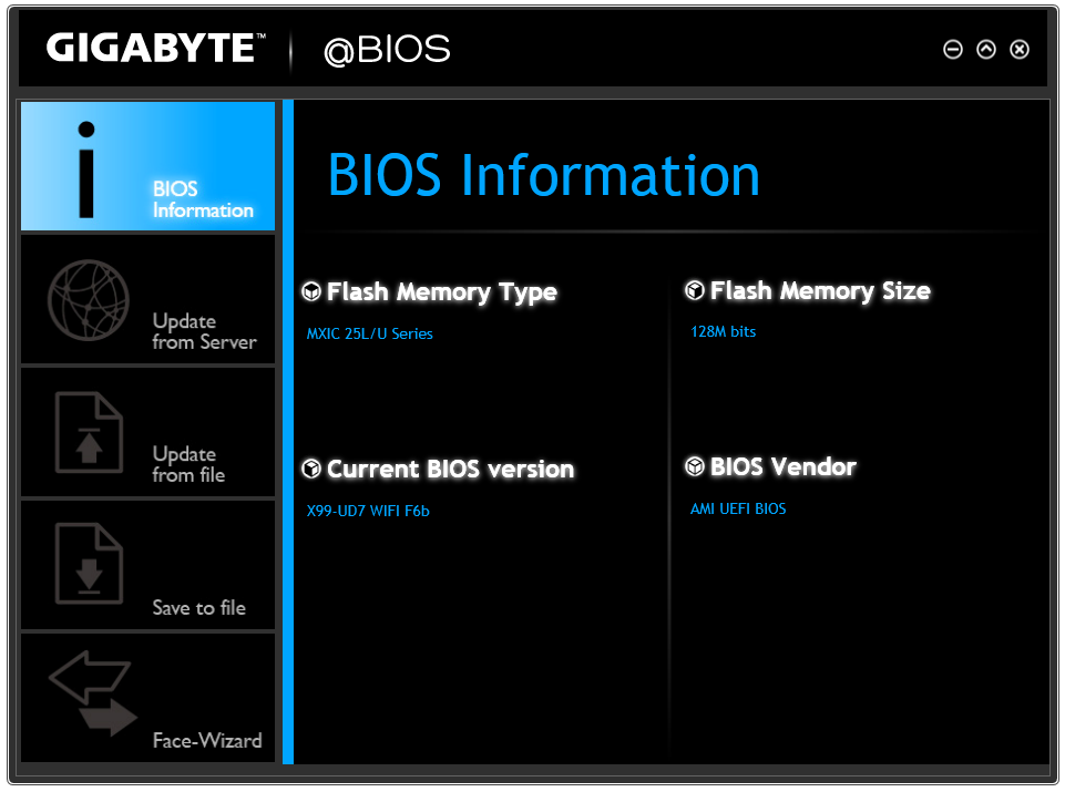
@BIOS is the interface for updating the BIOS through the operating system. This front screen shows the details of the motherboard (note the 128 Mb BIOS chip), and the tabs on the side allow the BIOS to be updated by directly downloading the BIOS from the server or via a file. The bottom selection, Face-Wizard, allows a user to adjust the POST image on startup.
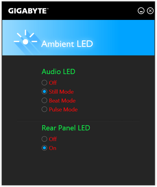
Ambient LED adjusts the lighting for the rear panel and the heatsink on the motherboard at the same time. In still mode both lights are on constantly, with pulse having the lights phase in and out. Beat mode keeps track of audio coming through the speaker ports on the rear panel and adjusts its intensity based on the music playing. I tried with various artists and the lights to adjust depending on slow and fast music, although during fast music it comes across as very flashy.
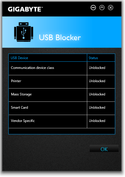
USB Blocker allows the administrator to block different types of devices used in the USB ports. GIGABYTE’s main use for this is in an office environment to stop employees using mass storage, or for public machines such as in libraries.
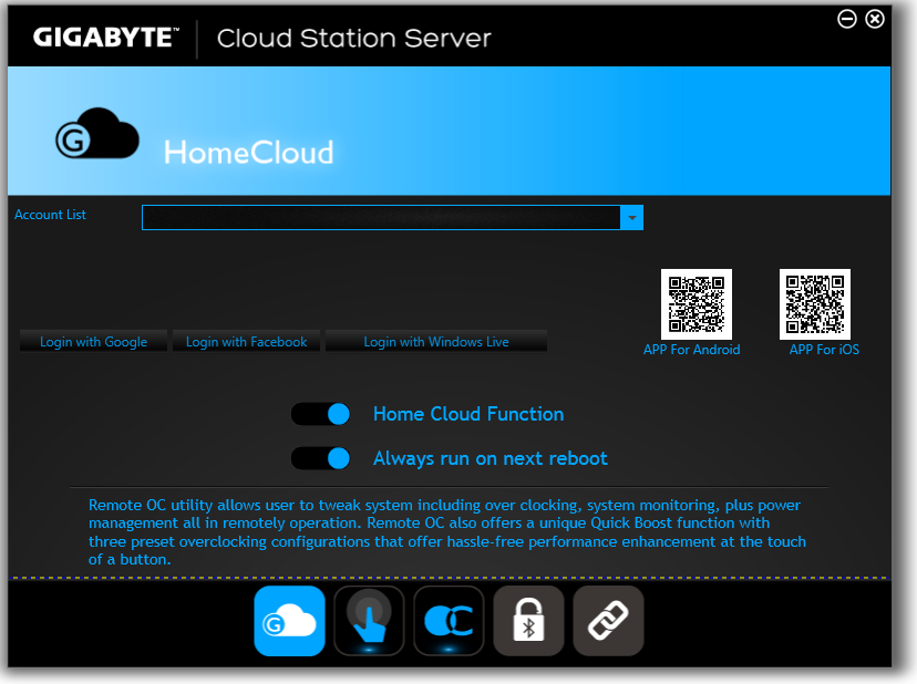
The Cloud Station Server is a relatively new part of GIGABYTE’s software package, allowing for overclocking, remote control, hotspot functionality and adjusting use based on proximity to a Bluetooth device (such that the system hibernates if >10m from a paired Bluetooth phone).

EasyTune is the big one for overclocking, and GIGABYTE offers several tools to help with automatic overclocks. We tested each of these and with a sufficient CPU 4.1 GHz should be a walk in the park. The Auto Tuning aspect also hit 4.1 GHz on our sample.
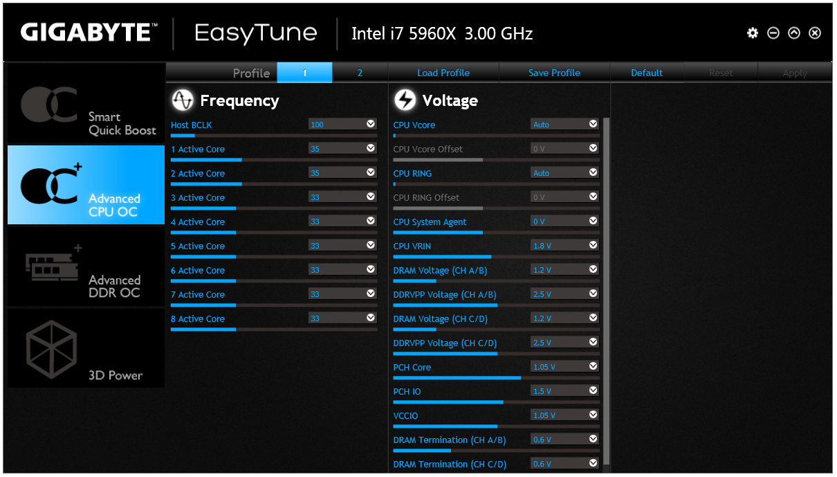
Manual overclocking can also be performed, and here GIGABYTE allows voltages by offset rather than the absolutes given in the BIOS.
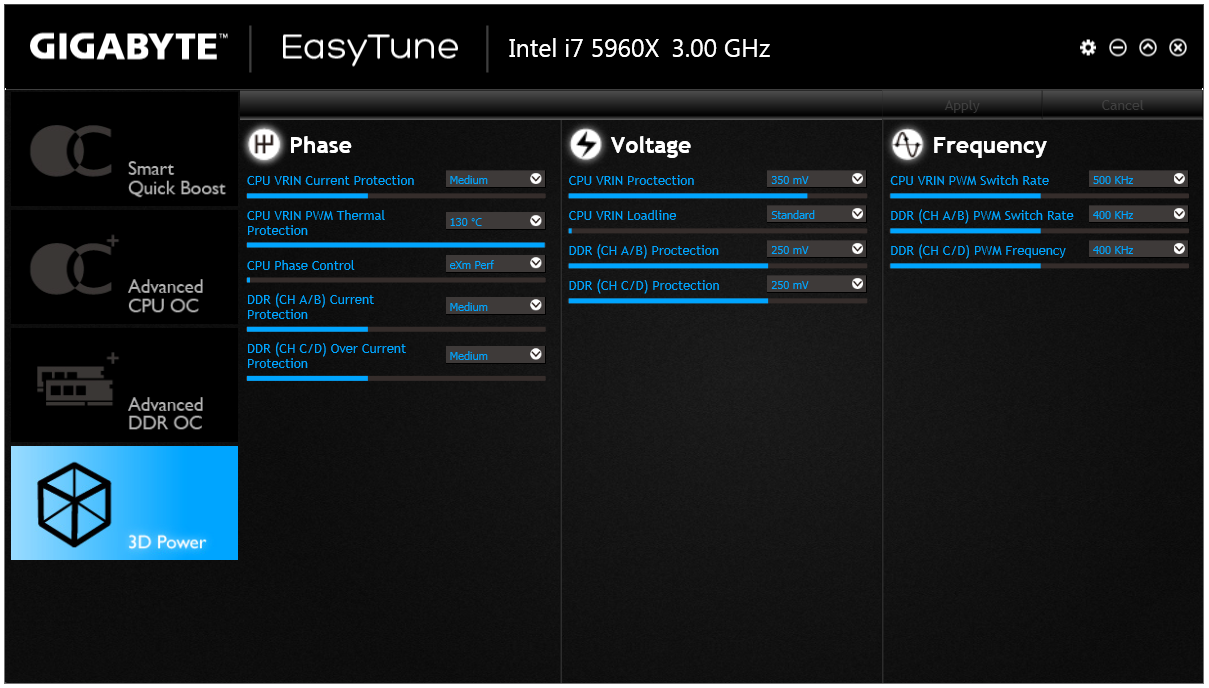
Users can also adjust the phase control and load line calibration in the 3D Power tab.
For users wanting to create RAID arrays using the chipset based solution, EZ Setup provides the tabs:
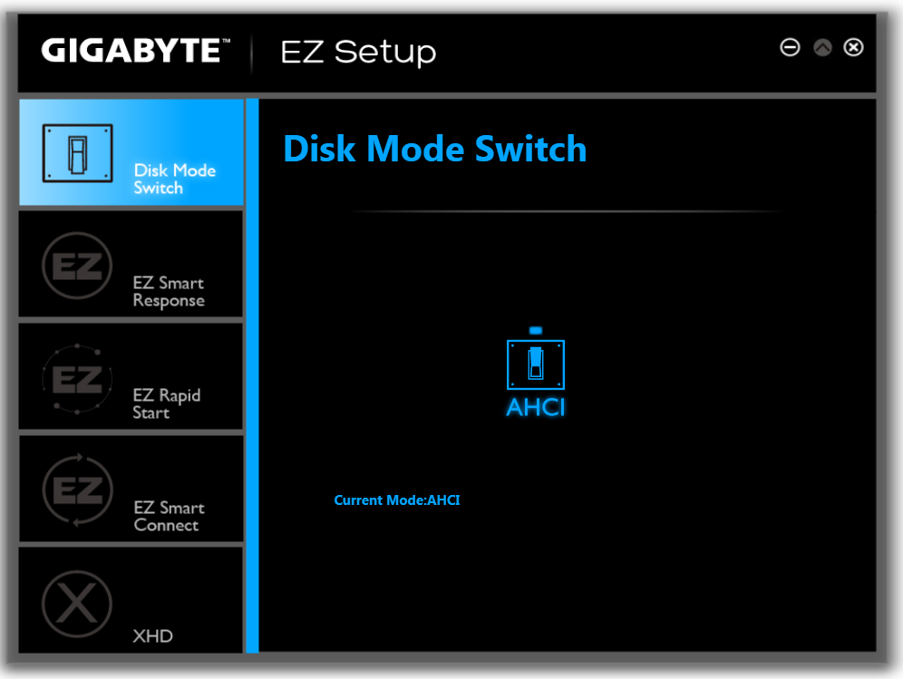
Ideally I would have liked this software to detect all the devices I have connected and list them, in case they were plugged into the wrong SATA ports for RAID as shown above. This software will also allow users to use an SSD as a cache for a large disk drive.

The Fast Boot application does what it says on the tin, with an extra option to allow users to restart and enter the BIOS directly.
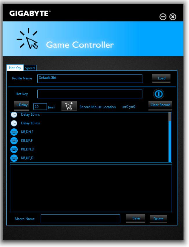
One of the newer tools in GIGABYTE’s arsenal is Game Controller, which allows both macro generation and introduces a ‘Sniper Mode’ for improved mouse accuracy. We have played with the macro generator before, and nothing much has changed – it needs some form of tutorial as well as the ability to adjust and move individual elements of the macro. Currently, if you make a mistake in making the macro, there is no way of adjusting a single element.
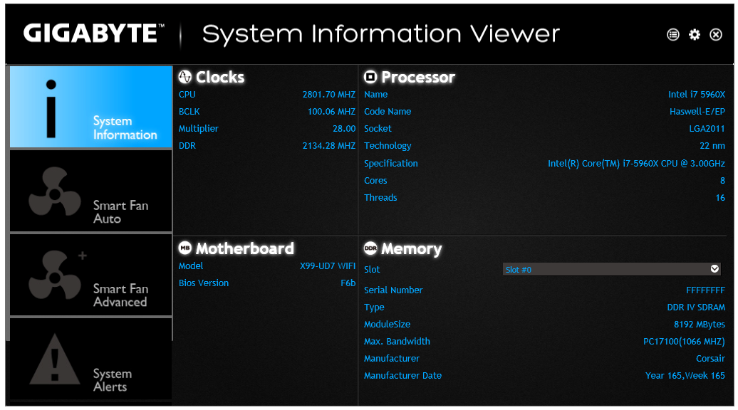
The System Information Viewer shows what the system has in it in terms of the processor, motherboard and memory, although the main use of this app is for the fan controls.
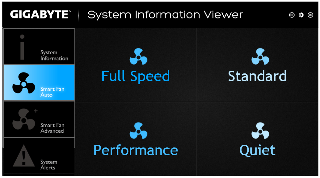
The software comes with four general fan settings which are applied to all the fans when selected.
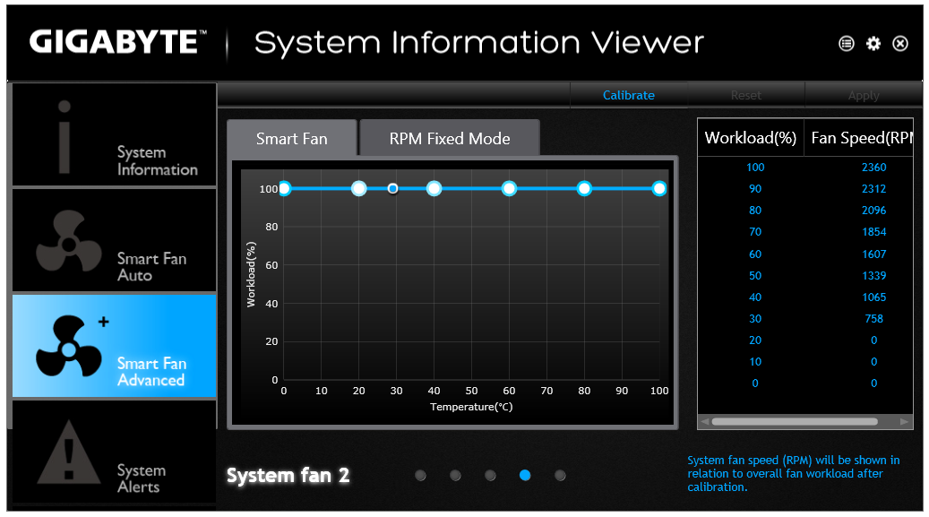
The advanced tab offers a calibration button that tests each fan in the system then the user can use that data to adjust the multi-point graph. That being said, I’m unsure why the software does not to the mathematics for the user such that we get a graph of fan speed against temperature – it would be really easy to do. GIGABYTE should also consider adding hysteresis to the fan configuration, as this allows the fan to remain at high mode when cooling down in order to speed up the process.
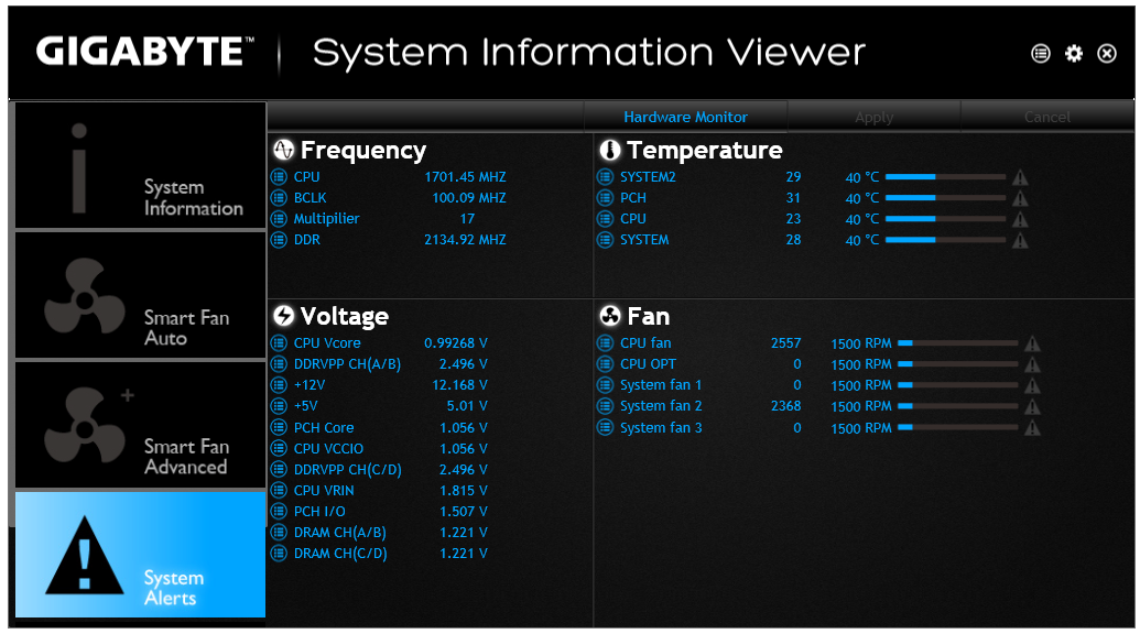
A user can also adjust the system to provide alerts when the temperatures or fans reach a maximum value. Other manufacturers provide similar alert systems, although typically users can select a high and a low value to produce a warning. The Hardware Monitor button here unfortunately did not work in our test system.
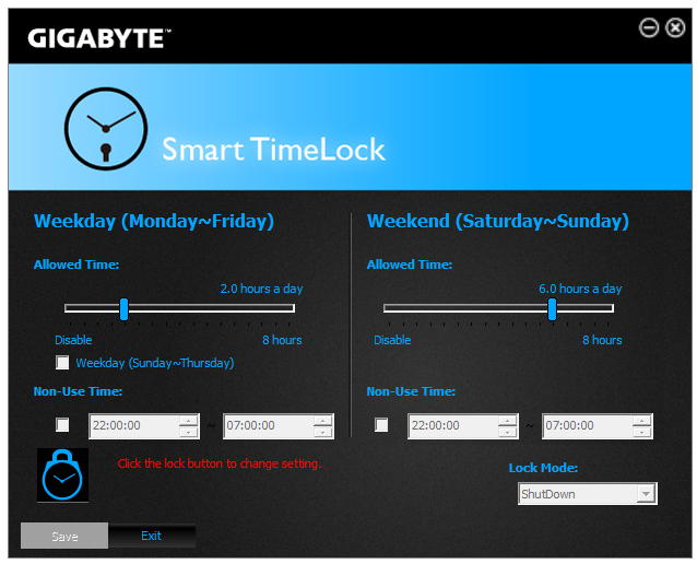
The Smart Time Lock feature is a super upgraded version of ASRock’s Online Management Guard but completely shuts down the system when the specified time limit is reached, or the system is in non-use time. This has applications for parents who want to limit the time their children use the computer for non-school activities.
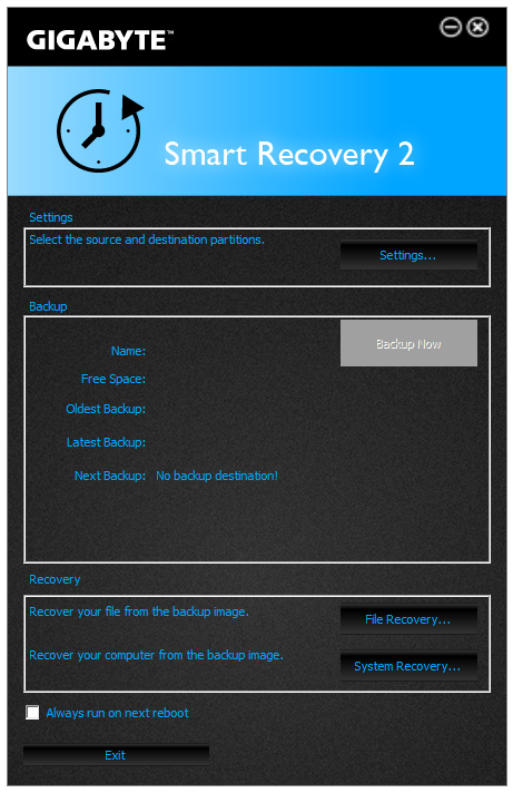
Smart Recovery will take an image of a drive for safe keeping and allow a user to restore he image should the system be compromised. Perhaps not ideal is that the user must install this software in order to restore the image – it would make sense if part of the software was baked into the image so it could self-extract and apply to the system it is run on.
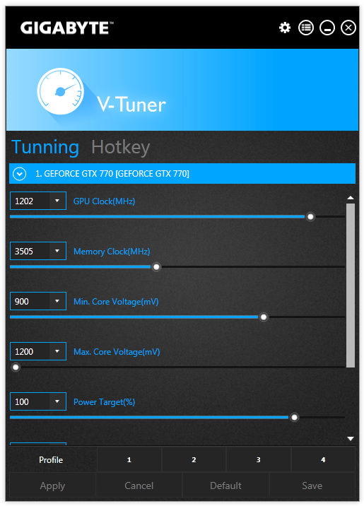
One feature we have not seen before is V-Tuner, which allows for GPU overclocking when applicable graphics cards are used. Here we had a non-GIGABYTE GTX 770 in play and it saw all the information as needed.
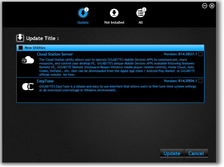
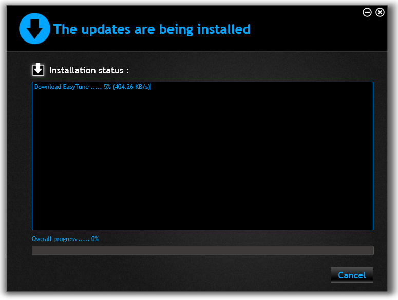
The last app for GIGABYTE is its update software. Compared to previous iterations we have tested, this successfully finds software that needs updating and performs the process of uninstalling and reinstalling as required. One issue that needs to be addressed here though is the size of each update needs to be made available to the user before it is selected to download. Otherwise those on slow or limited connections might be stranded with a 600MB update of audio drivers they might decide to postpone for another time.


ASRock X99 WS: The New
The clue is in the name, and ASRock’s WS line is aimed at workstation like builds. Historically we are more accustomed to ‘WS’ being another manufacturer’s product, but it would seem that terms like ‘Gaming’ and ‘Formula’ are now being wielded by many of the motherboard players. This is not ASRock’s first WS product – ASRock Rack has a number of WS products mostly based on server chipsets, but the Z77 WS and Z97M WS are still part of that product line.
ASRock’s big plug with the X99 WS is going to be workstation level features. This means a supersized heatsink, an enhanced power delivery system to improve efficiency as well as longevity while using a 160W processor and a total z-height sufficient to allow the motherboard to be included within a 1U chassis with an appropriate heatsink. ASRock is also claiming DDR4 ECC and RDIMM support with Xeon processors, dual Intel NICs (I217-LM with vPro and I210-AT) and support for 4-way PCIe devices. Ultra M.2 x4 with PCIe 3.0 is supported, although this reduces PCIe bandwidth of a fourth PCIe device.
Despite the WS name, the motherboard does support the Core i7 processors and non-ECC UDIMMs, although ASRock’s main selling point will be the combination of their consumer platform (BIOS + software stacks) while still having Xeon + ECC RDIMM support for a workstation. This is compared to a server, as this motherboard does not support LRDIMMs, although the 1U z-height integration means that it can be server capable. One limitation, or benefit depending how it is looked at, will be the use of X99 rather than the C612 chipset.
Regular functionality comes in the form of 10 SATA slots (all from the chipset), a TPM header, two COM headers (for WS), six fan headers, a Thunderbolt header, Realtek ALC1150 audio under Purity Sound 2, six USB 3.0 ports, an eSATA port and the extra PCIe power supplied by two molex connectors. Relatively new to ASRock from Z97 and carried to X99 is the HDD Saver feature, allowing users to connect two SATA drives via the included cable and power these drives down while in the OS in order to keep them safe from viruses that corrupt data or improve longevity by only being enabled when needed.
All of this will retail for $324, and aims to be one of the cheapest ‘WS’ X99 motherboards on the market. The only issue there is that some other manufacturers might not advertise Xeon support, but the QVL lists will confirm this. ASRock’s claim then comes from the workstation level equipment on board (power delivery, dual Intel NIC), the BIOS and software ecosystem, and that these other Xeon-capable motherboards might not be ECC/RDIMM capable.
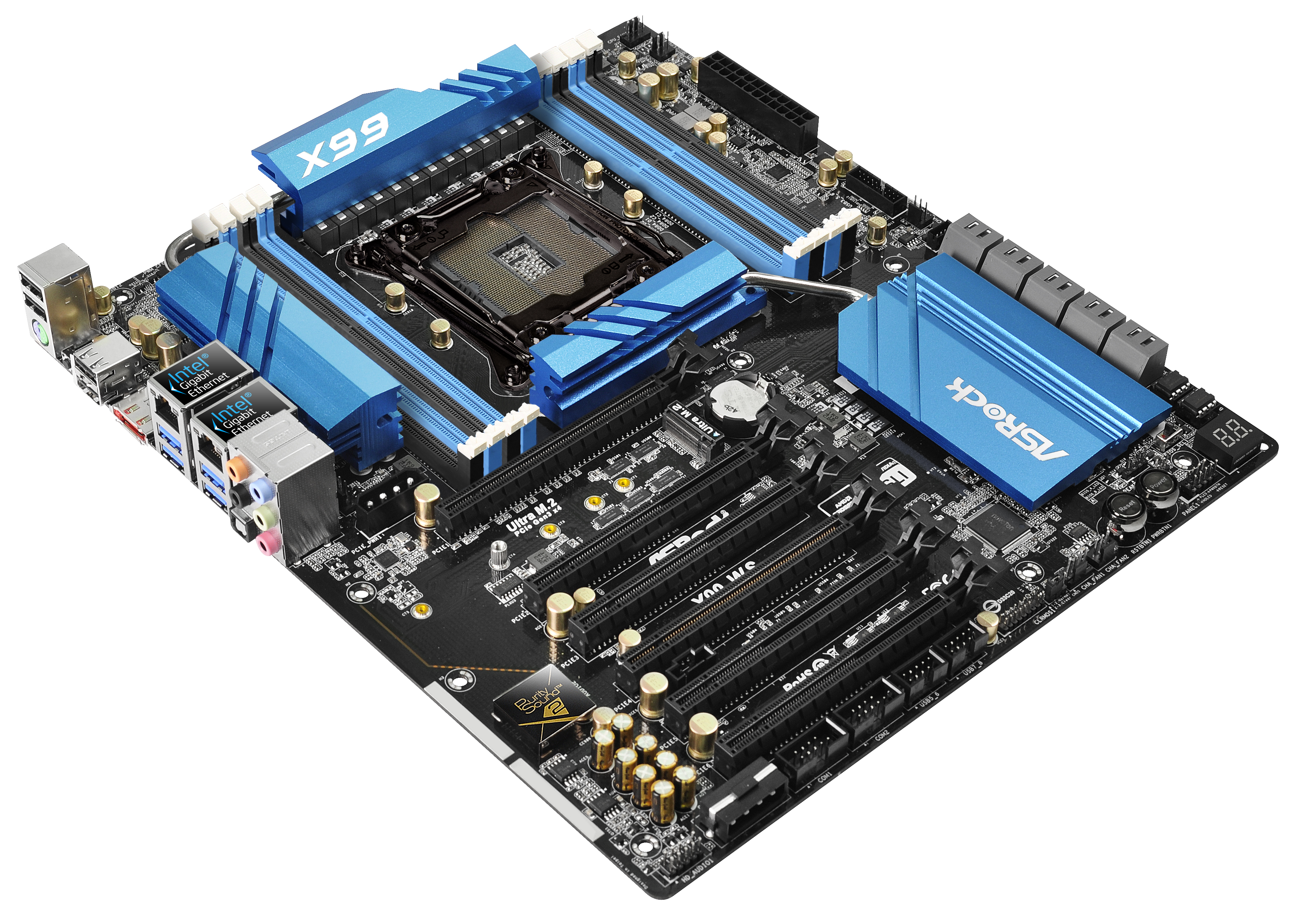
ASRock X99 Visual Inspection
ASRock’s ‘XXL’ power delivery heatsink design uses a total of four heatsinks, connected in pairs. The big addition is the heatsink to the left of the DRAM slots – while it covers some of the ICs in that region, its main purpose is to provide more bulk and surface area to aid in cooling the twelve power phases underneath the heatsink at the top. If you were not sure what chipset is being used here, the big X99 logo at the top tells you.
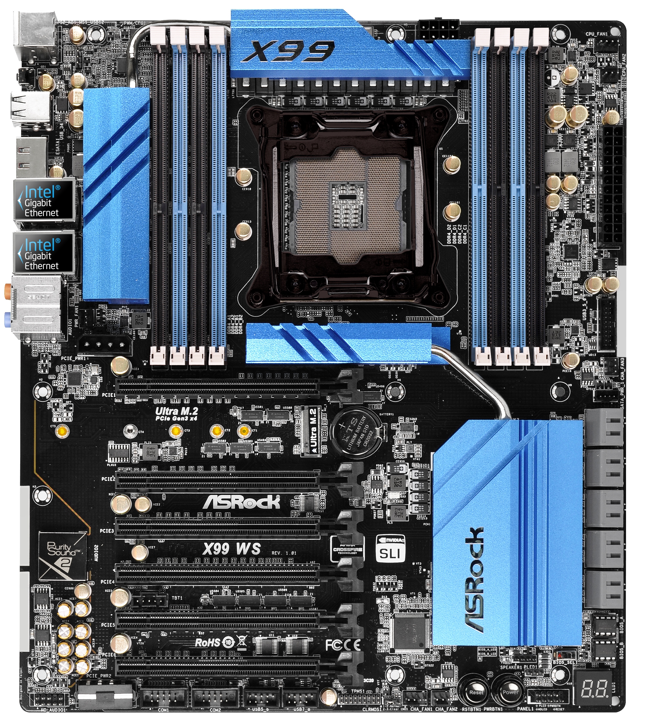
The X99 WS uses a two DIMM-per-channel design, with the slots having a single sided latch design due to the close proximity of the first PCIe slot. The DRAM slots are color coded, though nothing specifically tells the user to use the black slots first. I would assume that when the user is in 1DPC mode, this allows the blue color to come though.
The socket area has access to four fan headers: two in the top right, one just above the PCIe molex power and another below the USB 3.0 header. The final two are at the bottom of the motherboard. Out of these six, only two of them are 4-pin headers which is perhaps a little disappointing.
Beneath the USB 3.0 header on the right hand side of the motherboard is the HDD Saver header for the cable included in the box. The ten SATA ports then follow, with RAID supported on the six SATA3_x ports rather than the four S_SATA3_x ports. The S_SATA3_3 connector is shared with the eSATA port on the rear, meaning only one can be used at a time. Ideally I would have liked ASRock to color code the SATA ports, indicating which are RAID capable and which were not. Notice there is also no SATA Express here, perhaps indicating how ASRock feels the storage market is evolving.
The somewhat large chipset heatsink is above a BIOS select switch next to two removable BIOS chips. Power and reset buttons are handy to have on any workstation/server motherboard, and these are included here in the bottom right hand corner as well.
As workstation users can work with any number of requirements, ASRock has included a TPM header as well as two COM headers, with two USB 2.0 headers in-between.
The PCIe layout is geared towards four-way GPU/PCIe device layouts, although the configuration differs depending on using a 40 lane PCIe processor or a 28-lane PCIe processor (such as the i7-5820K) with the following arrangements:
40 Lane PCIe: PCIe 1/2/3/4/6 at x8/x8/-/x8/x8
28 Lane PCIe: PCIe 1/2/3/4/6 at x8/x8/x4/x8/x0
PCIe 5 uses four lanes from the PCH, while PCIe 1 and 4 use 15 micron gold connectors as these are used for the first two GPU slots. Interestingly, when four-way GPU is used with a 40 PCIe lane processor, the system does not enable the full 40 lanes (x16/x8/x8/x8). This would suggest that the motherboard lacks the additional external clocks required to enable this orientation, while the ASUS and GIGABYTE motherboards in this review have this feature. That being said, we have not seen a use case where x16/x8/x8/x8 wins out against x8/x8/x8/x8. More investigation would be needed.
Another point of contention for the PCIe layout will be the source of additional PCIe power. While having two extra sources of power is appreciated, the fact that it comes from a molex connector is unfortunately short-sighted. Molex connectors are bulky, and the top power connector being in the middle of the board is frustrating. It means stretching a cable over most of the motherboard, destroying any potential aesthetic and potentially disrupting the airflow.
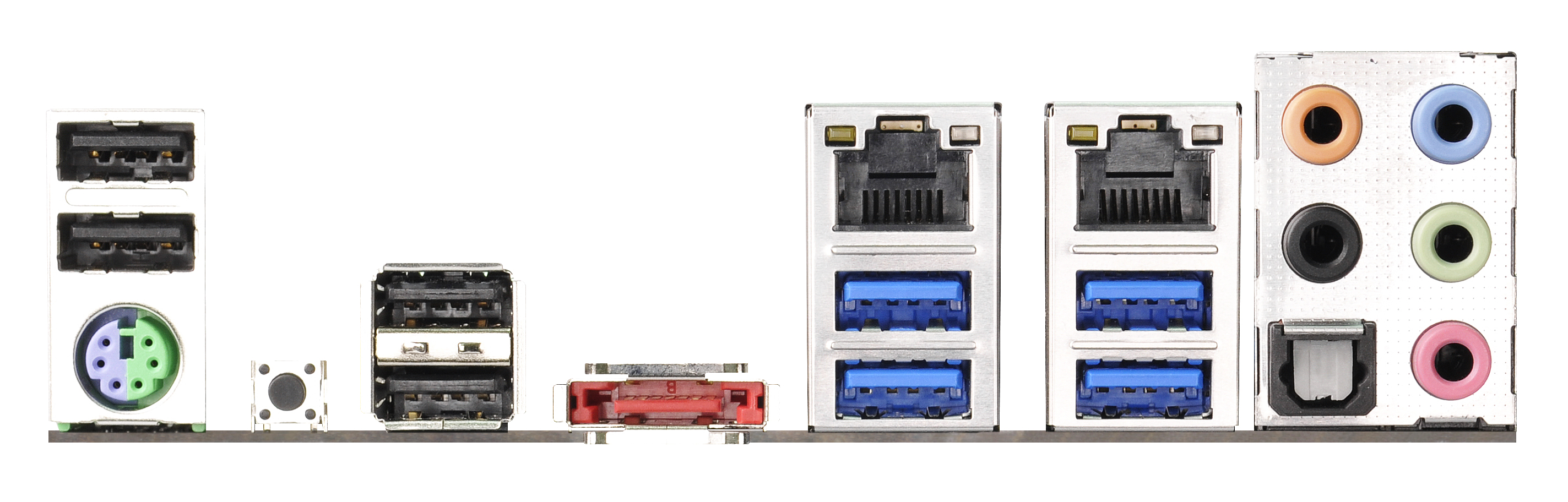
The IO panel is basic for an X99 platform but covers the bases: a PS/2 combination port, four USB 2.0 ports, four USB 3.0 ports, a ClearCMOS button, an eSATA port, two Intel network ports and a set of audio jacks from the ALC1150 codec.
ASRock X99 WS Board Features
| ASRock X99 WS | |
| Price | US (Newegg) |
| Size | ATX |
| CPU Interface | LGA2011-3 |
| Chipset | Intel X99 |
| Memory Slots |
Eight DDR4 DIMM slots, up to Quad Channel 128GB 1600-3200 MHz Non-ECC UDIMM ECC/RDIMM at JEDEC |
| Video Outputs | None |
| Network Connectivity |
Intel I217-LM (vPro enabled) Intel I210-AT |
| Onboard Audio | Realtek ALC1150 via Purity Sound 2 |
| Expansion Slots |
5 x PCIe 3.0 x16 - 40 PCIe Lane CPU: x16, x16/x16, x16/x16/x8, x8/x8/x8/x8 - 28 PCIe Lane CPU: x16, x16/x8, x8/x8/x8, x8/x8/x4/x8 1 x PCIe 3.0 x4 (Shared with M.2) |
| Onboard Storage |
6 x SATA 6 Gbps, RAID 0/1/5/10 4 x S_SATA 6 Gbps, no RAID 1 x Ultra M.2 3.0 x4 |
| USB 3.0 |
4 x USB 3.0 Ports, Rear IO 1 x USB 3.0 Header |
| Onboard |
10 x SATA 6 Gbps 1 x USB 3.0 Header 2 x USB 2.0 Headers 6 x Fan Headers 2 x COM Headers 1 x TPM Header Power/Reset Buttons Two Digit Debug HDD Saver Header Thunderbolt Header Front Audio Header Front Panel Header BIOS Select Switch |
| Power Connectors |
1 x 24-pin ATX 1 x 8-pin EPS 12V CPU 2 x 4-pin Molex for PCIe |
| Fan Headers |
2 x CPU (4-pin, 3-pin) 3 x CHA (4-pin, 2x 3-pin) 1 x PWR (3-pin) |
| IO Panel |
1 x Combination PS/2 Port 4 x USB 2.0 Ports 4 x USB 3.0 Ports ClearCMOS Button 1 x eSATA 6 Gbps 2 x Intel GbE Network Ports Audio Jacks |
| Warranty Period | 3 Years |
| Product Page | Link |
I am not sure how I feel about the $324 cost of this motherboard. For the most part we are getting the basics, whereas we get something different with the GIGABYTE around the similar price and something more with the ASUS at $400. ASRock would counter this and point to the server grade components. It seems odd to discuss a more expensive ASRock board without extra functionality you can physically use, although the use of a vPro enabled NIC does allow for Windows Server applications.
ASRock X99 WS BIOS
The ASRock BIOS shifted slightly between Z87 and Z97, and it is the Z97 implementation we get on X99. This means the starry background is gone, replaced with a dark and blue-crystalline image. The icons are also reduced to mere text with a small image, and unlike the ASUS BIOS the menu sections are of equal size, which I prefer. There is also an adjustment to the OC Tweaker layout, which we will come to.
There is no ‘Easy Mode’ for the ASRock BIOS, with entry direct into this first Main screen. The right hand side of the BIOS is for description of the option selected, and the main segment shows information such as the BIOS version, CPU installed, CPU speed and memory installed. As mentioned in previous reviews, having some set of information relating to CPU voltages, temperatures and fan speeds might be useful here. If ASRock was to do an Easy Mode, it would make sense to have a one-button overclock option as well.
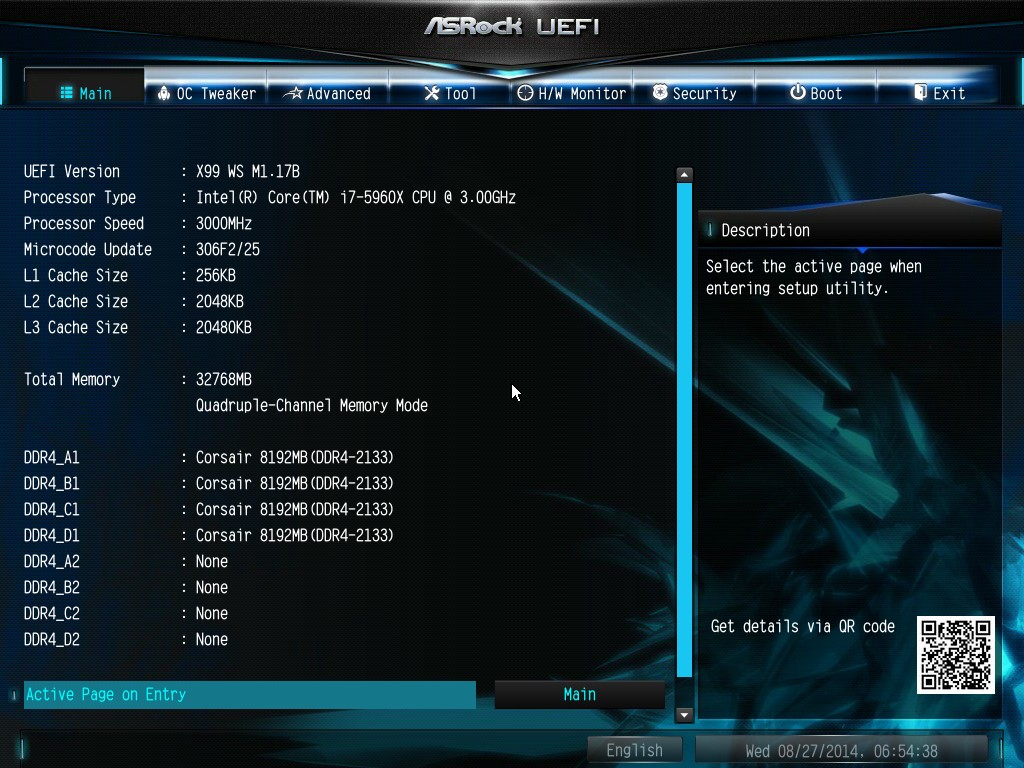
At the bottom of this page is an option to select the entry page, allowing overclockers to go straight into OC Tweaker.
OC Tweaker takes heed of one of my previous complains about the ASRock overclock options. Previously there used to be a long list of options that continuously grew, depending on what options were left open to the user. For X99, ASRock has condensed these options into separate submenus similar in design to those we see on a GIGABYTE motherboard. Note that ASUS and MSI BIOSes currently go half-way between these extremes, offering some basic options with the more advanced ones in separate menus.
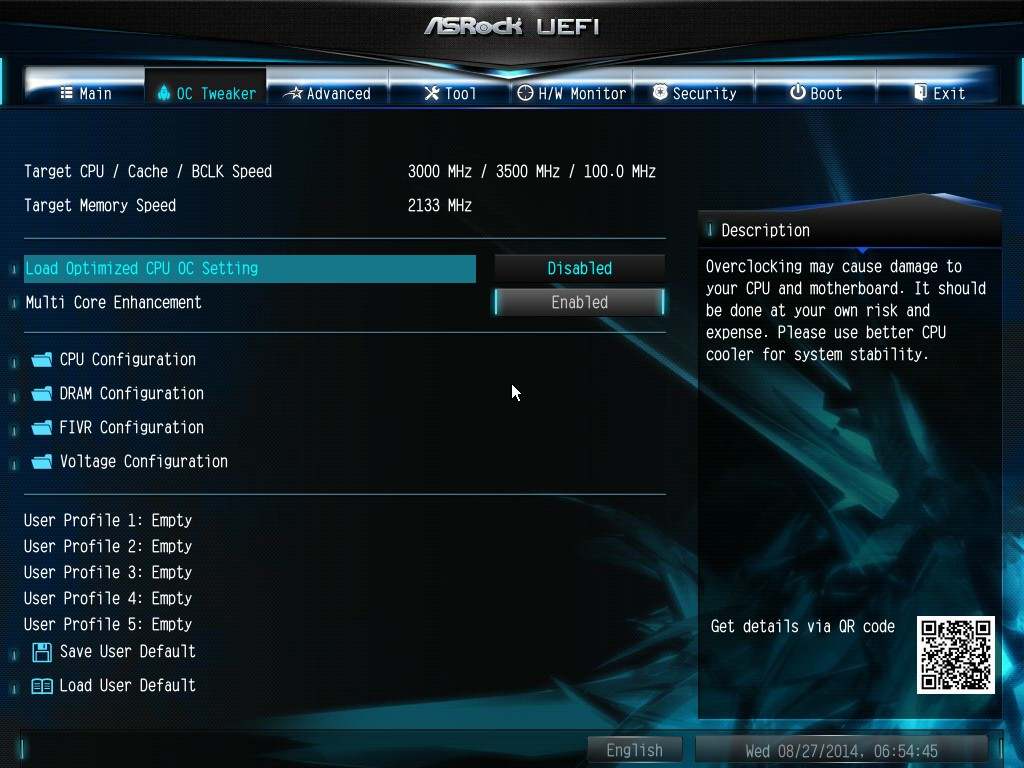
ASRock cuts straight to the chase – the first two options deal with overclocking. We have touched on features like Multi Core Enhancement many times previously, but it is interesting to have it so high up on the list of options. The Optimized CPU OC Setting gives some easy selections for overclocks based on ASRock’s internal testing:
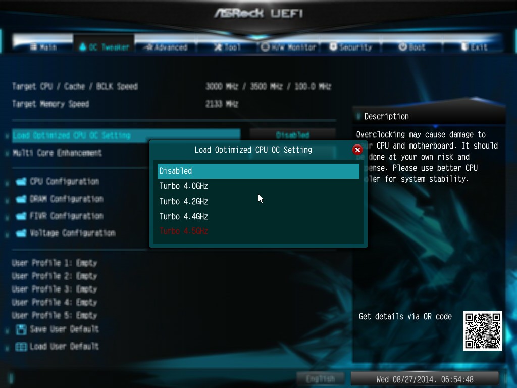
In line with our overclock testing, 4.0 GHz and 4.2 GHz should be achievable by all CPUs, with 4.4 GHz by most and 4.5 GHz by around half, given sufficient cooling methods.
The OC Tweaker menu is split into four sections. CPU Configuration gives options for CPU Ratio, multiplier, frequency, turbo boost and power limits:
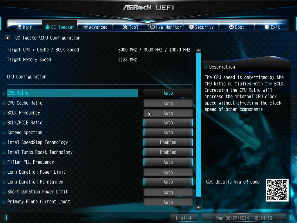
DRAM Configuration allows for XMP application, DRAM strap adjustment, DRAM voltage and sub-timing adjustment, all the way through primary timings, secondary timings, tertiaries and others.
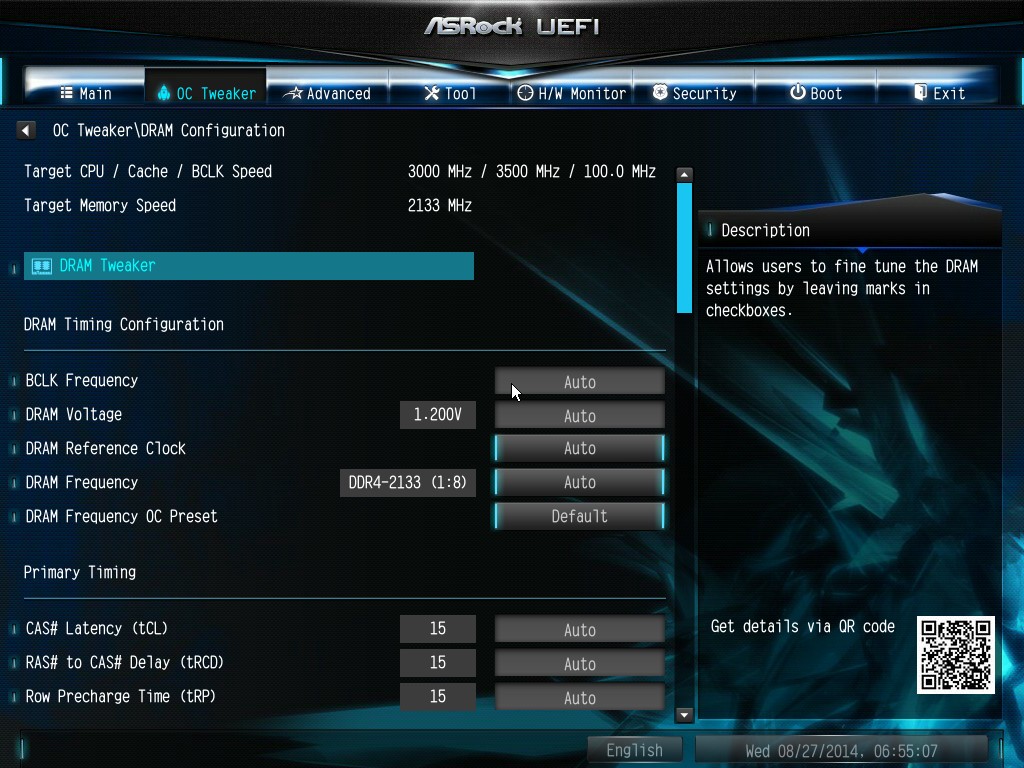
ASRock still uses the DRAM Tweaker function to fine tune the JEDEC and XMP responses to each memory kit:
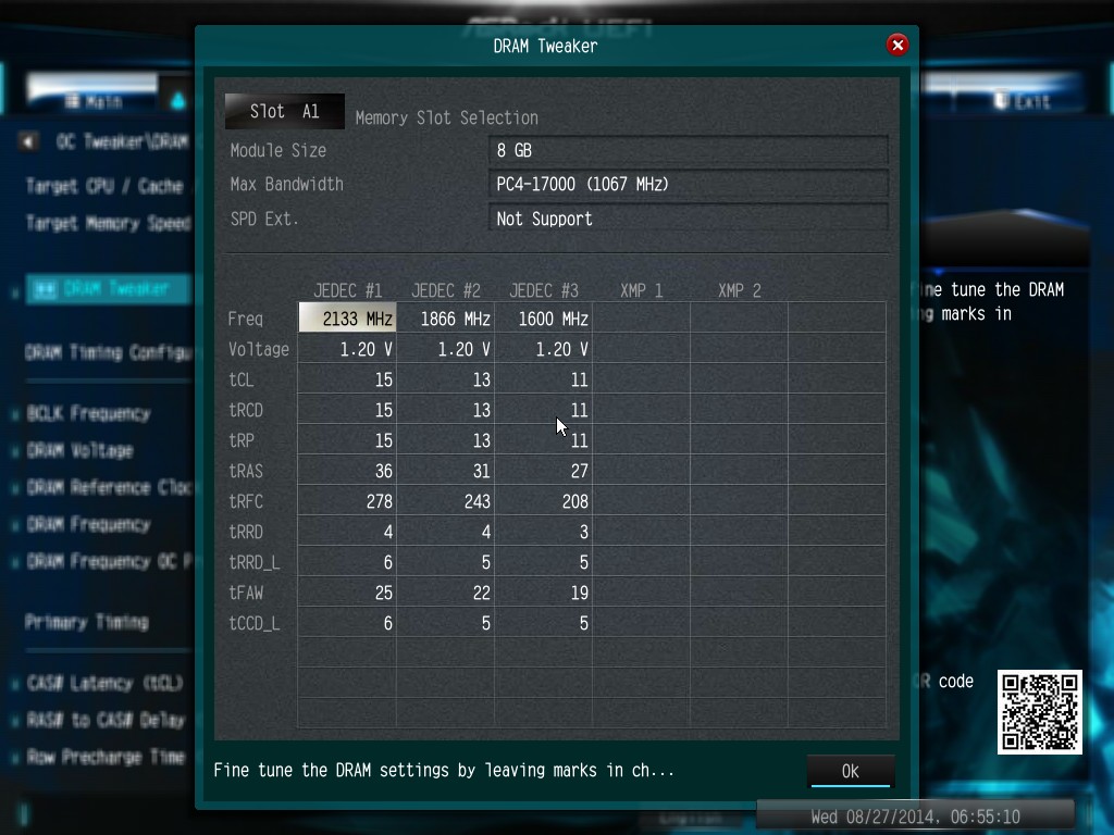
The ASRock BIOS also offers a DRAM Frequency overclocking preset list which will adjust the CPU strap and BCLK frequency needed to achieve various speeds:
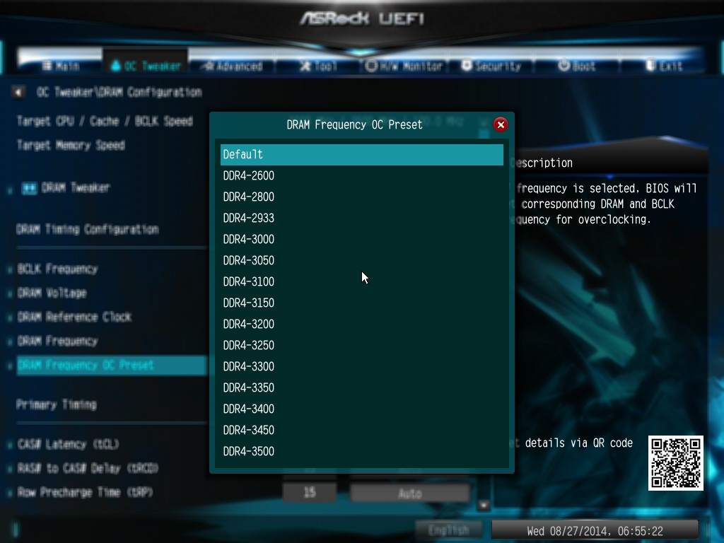
The FIVR Configuration menu from the OC Tweaker page deals primarily with the CPU and CPU Cache/uncore voltages.
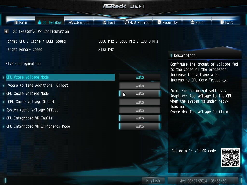
The Voltage Configuration menu has the other voltages on the system, including VCIN to the FIVR and load line calibration. The Load Line Calibration option also comes with a handy graph showing what each setting means:
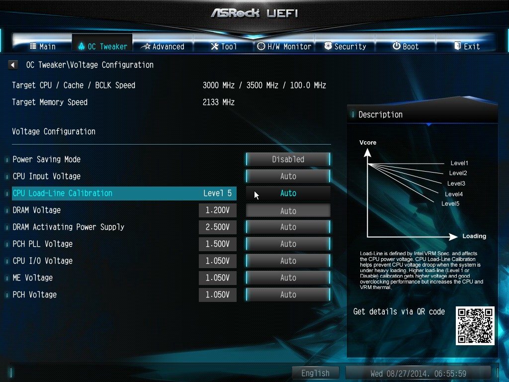
Unfortunately this arrangement of voltages is mildly confusing. Typically an overclocker will adjust the CPU voltage and the Load Line Calibration settings enough to get the right combination, and ASRock has placed these options in two different menus. If the CPU VCore option could be duplicated in the Voltage Configuration menu, this would be preferable.
The Advanced tab deals with other elements of the system configuration, such as the chipset, storage and super IO calibrations. This includes fixing power modes, PCIe linking speeds, disabling or enabling onboard controllers and adjusting RAID configurations.
By default the Thunderbolt header is disabled, and I am surprised not to see an option here to enable Above 4G Decoding to allow PCIe co-processors like the Xeon Phi range to be used in a Workstation product. I am hoping this is addressed in a further BIOS revision.
The Tools menu is typically where ASRock tries out its more unusual ideas, although we do not get anything new for X99 that we have not seen on Z97 already. The System Browser shows the different elements of the motherboard and what is detected:

The Online Management Guard allows the user to enable or disable the network ports at various times of the day, as determined by the system time:
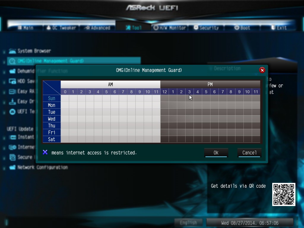
(It is amusing that this feature is aimed more at controlling when a child is allowed online, but X99 is not exactly a system configuration used as secondary machines.)
The Dehumidifier function now gets its own sub menu, allowing fans to spin for a fixed time after the machine is in S5:
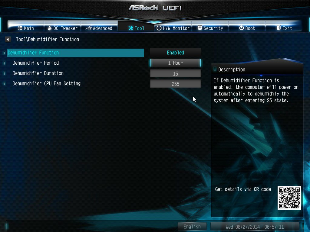
HDD Saver also gets slightly more explanation. A new feature to ASRock from Z97, using the bundled cable to two SATA power ports, a user can enable or disable the power to two SATA devices connected. This allows the drives to only be turned on when needed, potentially saving power, increasing longevity of the drives and saving the drives from potential harm that renders stored data unusable.
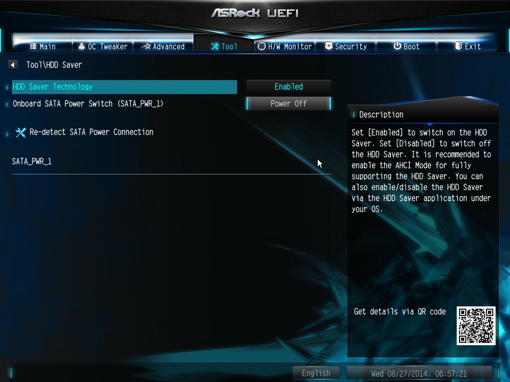
The H/W Monitor tab is where the temperatures, fan speeds and voltage monitoring tools are all kept, and although we have seen an effort by the other manufacturers to improve the fan control situation, ASRock is still relying on a simple option select procedure. For example, a user can put a fan into one of five modes:
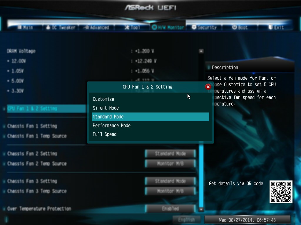
In the custom option, we get a series of selects for a multi-point gradient:
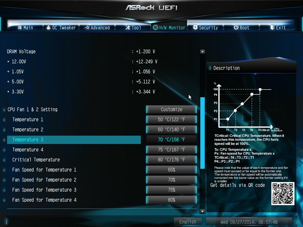
There is also an option to select which temperature sensor is being read from to make these adjustments:
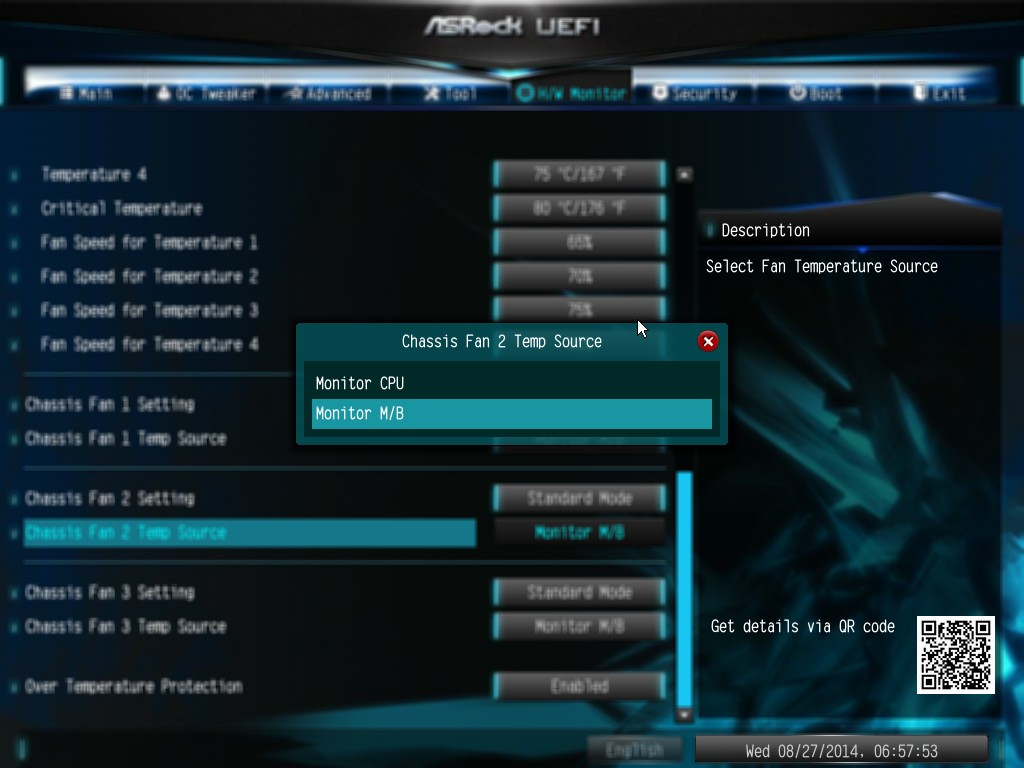
Now the whole point of a graphical user interface in the BIOS is so the user can interact with their options. ASUS and MSI are both well ahead on ASRock on this front. ASRock has the options there, but ASRock needs to write some code to allow the user to adjust the fan gradients by interacting with a graph, not by selection options from a drop-down menu.
The rest of the BIOS deals with security, boot order and fast boot options. In the Save and Exit menu we do get options for Boot Override:


ASRock X99 WS Software
The software package from ASRock has gone through a slow evolution since Z77 into a single interface for all of ASRock’s functionality called A-Tuning. With the overclocking and gaming models the interface is slightly adjusted, but the green tint follows the majority of ASRock’s motherboard range. However the newest element to ASRock’s like is the APP Shop. This is essentially ASRock’s curated version of the Play Store/Microsoft Store, with only software ASRock feels is suited to their motherboard range.
Currently the software is fairly limited to Chrome, ASRock’s own software programs and a few Asian free-to-play titles. While offering this method to obtain software is interesting, it does open up a lot of questions. Will there be to-pay titles? What happens if one element of the store is filled with malware?
The APP Shop also offers a BIOS and Drivers section to update the system, but as of yet we have not had it working properly in our testing.
There is another update tool in A-Tuning.
A-Tuning
The initial interface revolves around overclocking, giving the following three modes for automatic frequency adjustments:
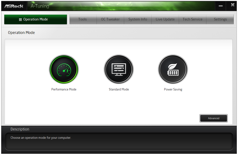
Power Saving puts the CPU into a low power mode (1.2 GHz on the 5960X) and requires the system have full CPU load before slowly ramping up the speed over the next 6-10 seconds. This keeps power consumption down, but perhaps delays the responsiveness of the system by not having that initial high single core frequency. Standard mode is the default setting, and Performance mode puts the CPU into high frequency mode for any loading. Performance Mode also opens up the Advanced menu:
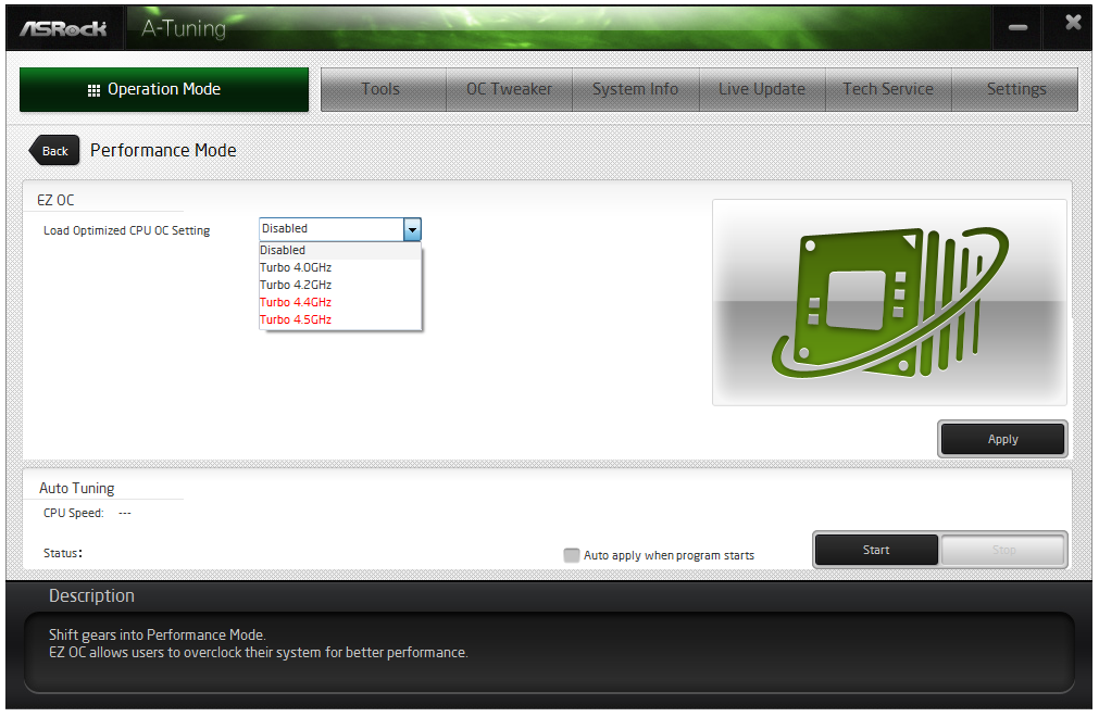
Here we have a list of Optimized CPU OC Settings similar to the BIOS and an auto tuning section. There is no list of auto tuning options similar to ASUS, for adjusting the stress tests or the optimum CPU temperature, although I would imagine that all the manufacturers might move in that direction at some point in the future.

The tools menu has a lot of space for ASRock to add in future features, but currently houses the ones they do have. XFast RAM allows the system to partition some of the RAM into a RAMDisk while also providing some RAMCache options:
XFast LAN is a customized interface for cFos, allowing users to prioritize certain applications over others:
Personally I find this interface extremely cumbersome, especially if there are a lot of applications to deal with. ASRock could design something with less white space and a more efficient amalgamation of the A-Tuning visual dimensions to make the process a lot easier. There is access to cFos directly with the Advance Setting button:
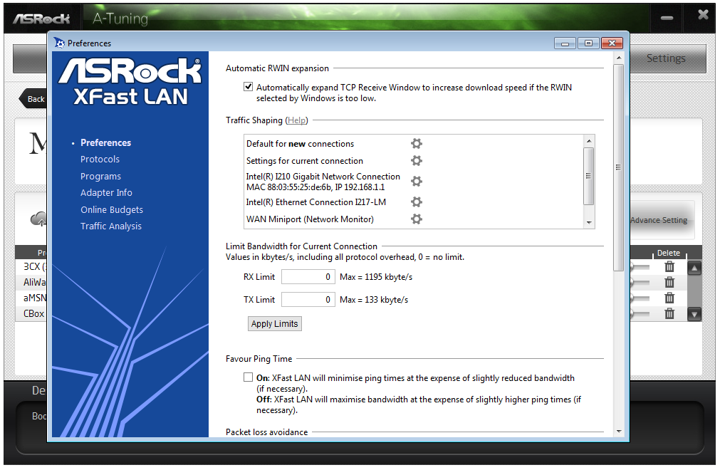
Fast Boot enables options relating to UEFI quick booting by disabling certain options until the OS is loaded:
The Online Management Guard has been around for several generations of ASRock motherboards now, and offers the user the ability to disable the networking ports during certain times of the day.
ASRock’s Fan software in the software is a lot easier to use than in the OS, giving a better sense for the user in what to adjust:
The FAN Test will detect the RPM for a given fan power, although the graph on the left is misnamed – what ASRock calls ‘FAN Speed (%)’ is actually deceptive because it means ‘Fan Power’ and the user has to do the mathematics in their head to adjust based on the table in the middle. If ASRock was on the ball, they would do the conversion in software and adjust the graph to read ‘Fan Speed (RPM)’ and adjust the axis appropriately from lowest Fan Speed to highest Fan Speed.
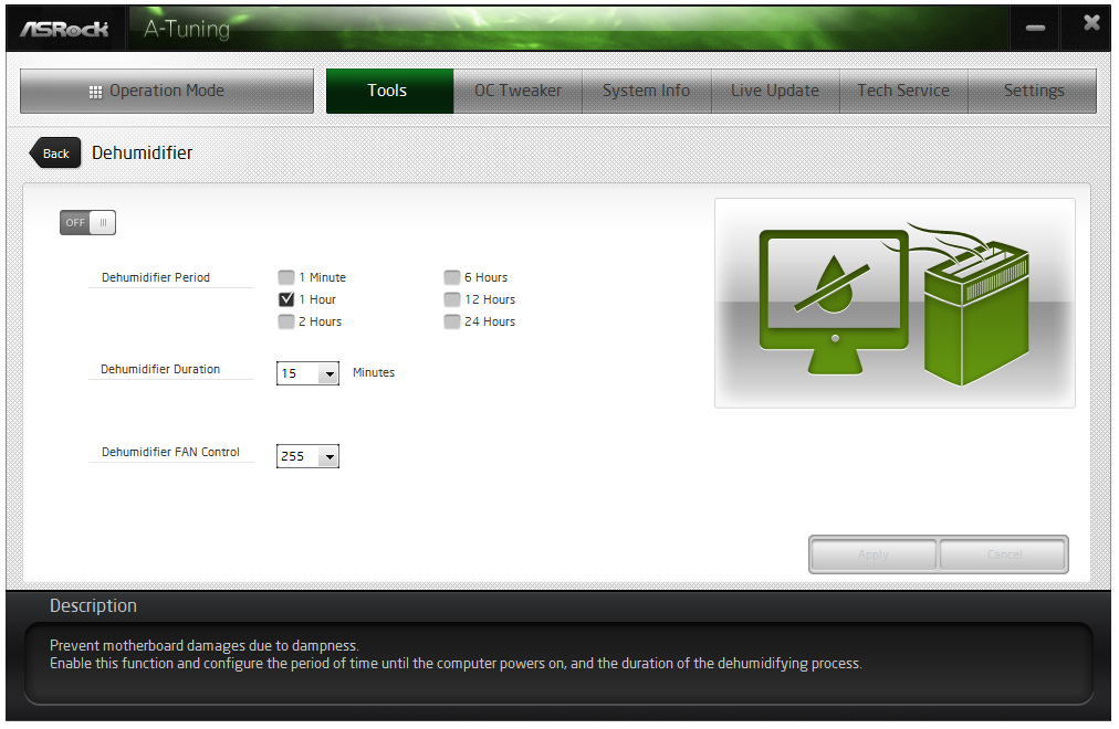
The Dehumidifier tool in the software is identical to that in the BIOS, allowing the system to enable the fans after the system has been shut off in order to equalize the air temperature inside and outside the case. This has benefits in humid environments where the moisture in the air may condense inside the case during a cool night after a hot day.
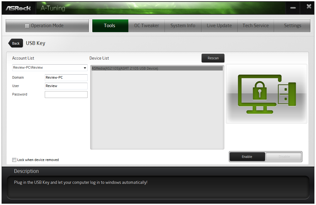
The USB Key tool allows users to assign a particular USB drive with login data for particular Windows users. This means that users need not remember a particular long password to log in, and only specified users are allowed to log in. Though lose the USB drive and lose the ability to log in.
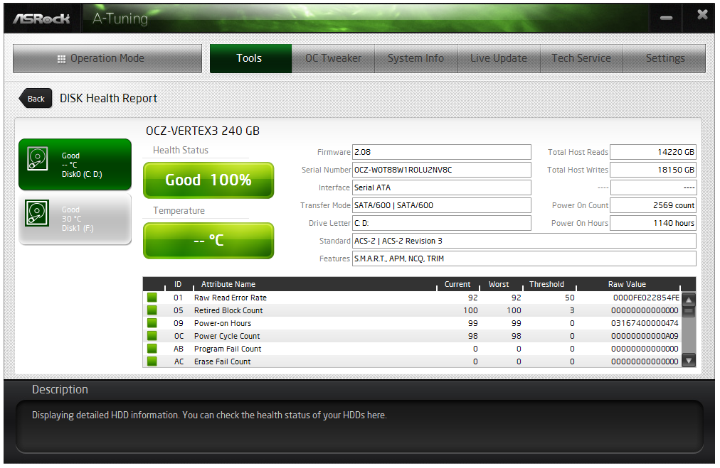
One of the newer tools in ASRock’s list is the DISK Health Report. This gives the critical information on the drives attached to the system, allowing SSD users to see the life of their drive. This drive has been at the heart of my motherboard test beds now for almost three years and is still going strong.

The next tab along the top is the OC Tweaker, featuring the more critical options from the BIOS for manual overclocking along with some options to save overclock profiles. The way this is shown in ASRock’s software is quite user-unfriendly, and I would suggest that the next iteration of the software gives an experienced user an easier way to adjust frequencies and voltages without dealing with sliding bars and scrolling.

The System Info tab gives the hardware monitor page by default, giving information about the frequencies, fan speeds and voltages in the system. Most other manufacturers have a way of recording this data, or seeing it plotted on a graph while running a stress test, but ASRock is behind at this time.
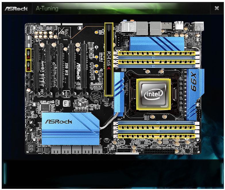
The Hardware Monitor section of System Info is identical to that in the BIOS, showing where hardware is installed with a mouse over giving basic details. This is handy for investigating which memory stick, USB or PCIe device is not being detected.
The Live Update tab is, by comparison to MSI, limited. Although I knew there were updates to the platform when I run this software, it failed to find the updated drivers. Here it also does not say how big each download is. If a user is on a limited or slow bandwidth package having to download 300MB of audio or graphics drivers can be detrimental.
While ASRock’s software package is presented in a good way, and there are a number of helpful tools, there are various aspects here that miss the mark in terms of user experience.


MSI X99S SLI Plus Overview
When MSI released shots of the X99S SLI Plus before the X99 launch, most of the comments were centered on one feature: the color scheme. Apparently there is something in the zeitgeist that likes an all-black color scheme, similarly to the popularity of other motherboards in the past but this time catering towards the more budget end of the market. The X99S SLI Plus will be MSI’s cheapest X99 motherboard in the first launch month, aiming at the $230 price point and eager to snap up some sales as a result.
As one might imagine, at such a low price point for X99, the SLI Plus does not come equipped with much in the way of ‘new to MSI’ features. The most poignant part of MSI’s product range is the ‘X99S’ nomenclature. The ‘S’ in that name indicates SATA Express support, and MSI is the only manufacturer actively advertising through the name of the motherboard that it has SATAe support. The state of SATAe as a whole is essentially up in the air right now – there are no consumer drives in the market and we are still a couple of quarters away from enthusiast adoption rather than mainstream adoption. The same could be said for M.2 however SATAe bandwidth must always come from chipset PCIe lanes or a controller powered by PCIe lanes, whereas M.2 can have bandwidth from the CPU PCIe lanes instead.
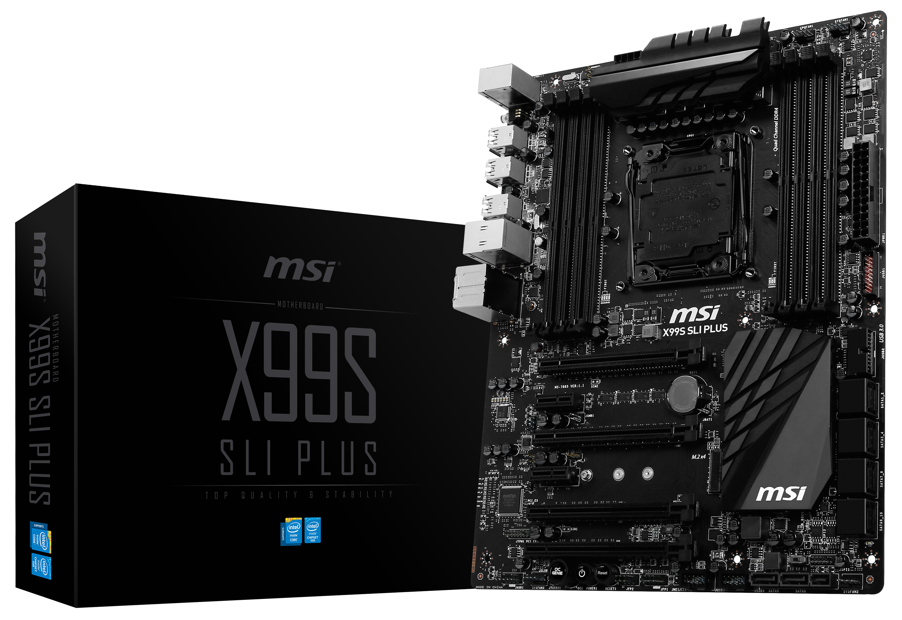
The M.2 on most of MSI’s X99 motherboards will be powered by four PCI 3.0 lanes from the CPU, giving a potential maximum of 32 Gbps when drives become commonplace. MSI’s motherboards will also come with an OC Engine, allowing for a continuous BCLK adjustment through 100-167 MHz and beyond, claiming lower jitter and power consumption, although MSI is not the only manufacturer to use this technique. As part of the MSI range as well, Military Class 4 and Guard Pro designations are being used, along with ECO Power to disable unused fan headers/PCIe ports to save power.
MSI X99S SLI Plus Visual Inspection
The most notable element of the SLI Plus when taking it out of the box is the color. There is something about a pure black color scheme that will make the modder in me reach for a can of spray paint ready to customize it. It does come across as a little bit odd when a motherboard has such a clean design (note, the reduced size socket to maximize the black color) and come in at the cheaper end of the scale.
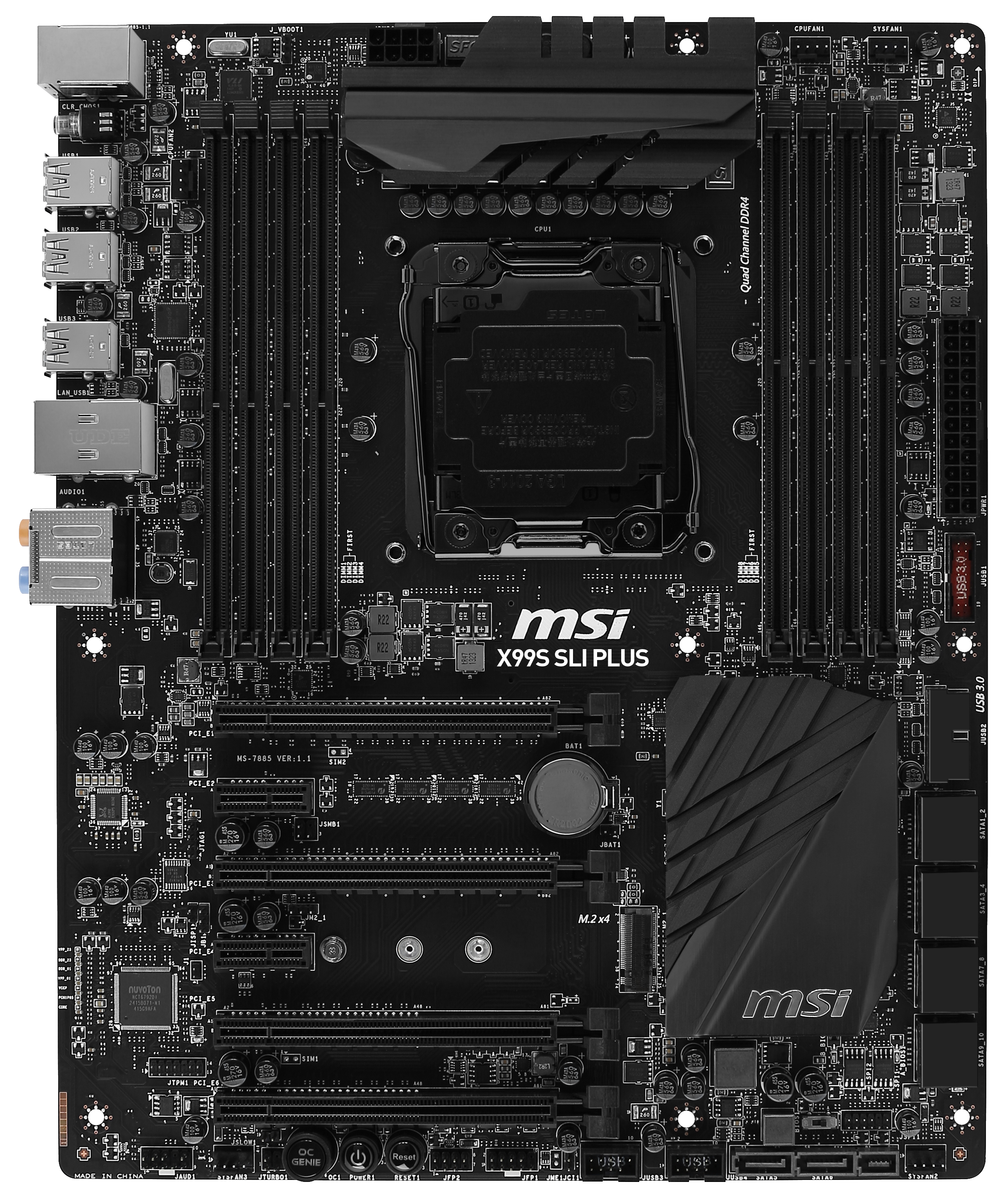
The CPU socket uses a design that focuses the connectors to the screws on the back panel, leaving the top of the motherboard free of big metallic bits to keep the continuity of the black color scheme. Unlike the other motherboards in this review, the heatsinks are not connected, relying on surface area for sufficient cooling. Due to placing all the DRAM slots in the black color, to help users place DRAM modules in the right order there is a diagram next to the DRAM.
The motherboard has five 4-pin fan headers, three within easy reach of the socket. One of these is on the left of the DRAM slots, next to the rear panel, with two more headers to the top right of the motherboard in the corner. The other two headers are at the bottom of the motherboard, one on the left and one on the right.
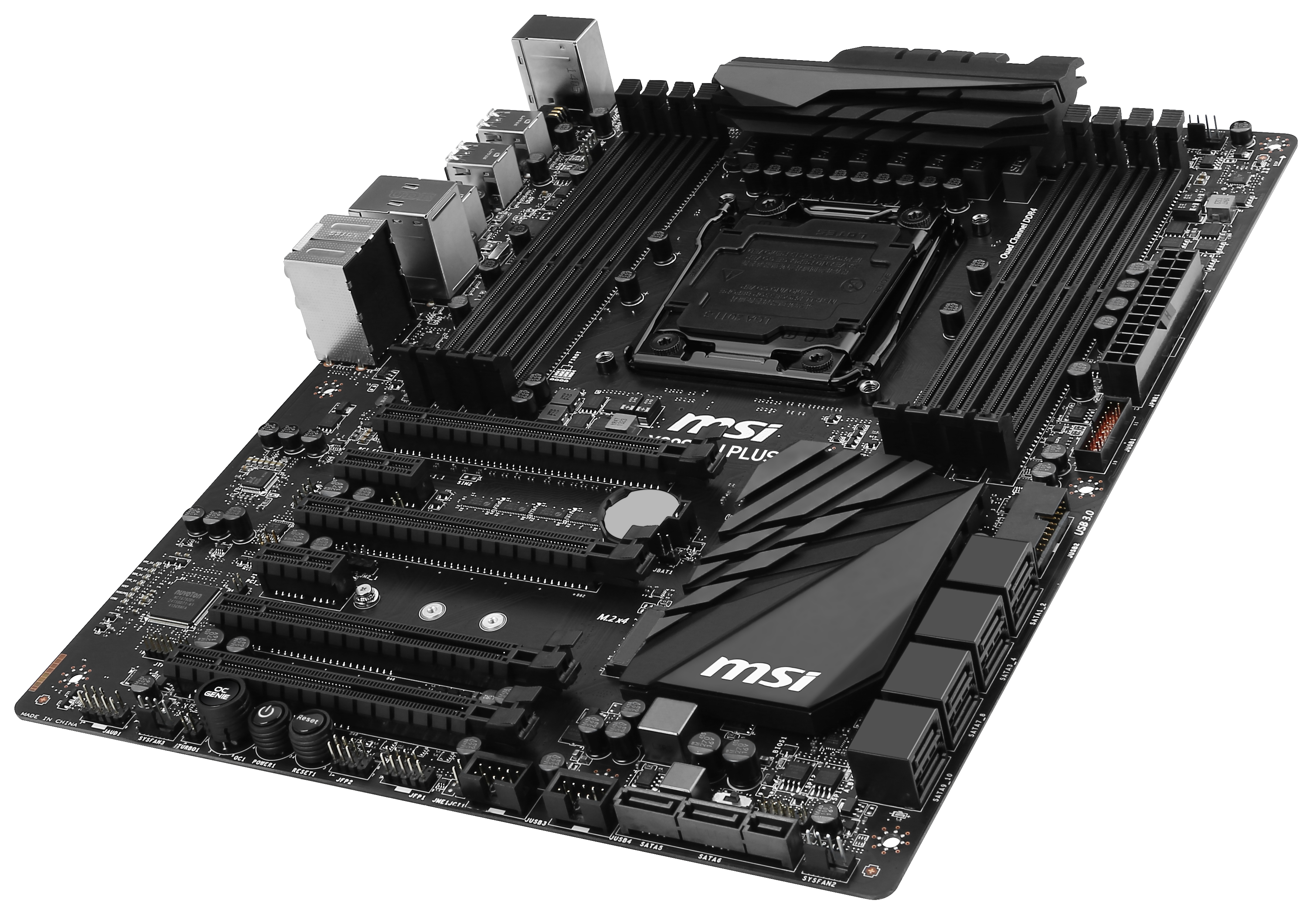
On the right hand side of the motherboard is a USB 3.0 header, with the inside in red indicating the fast-charge nature of the ports coming from it. There is another USB 3.0 header at right angles to the board similar to the SATA ports. Eight of the 10 SATA ports are next, and unfortunately MSI does not indicate which of these are RAID capable – normally I would suggest that either by port color or by name that RAID is easily identifiable, but MSI uses neither. (Actually SATA1-6 is RAID.) The final two SATA ports are at the bottom of the motherboard as part of the SATA Express connector.
The bottom of the motherboard is slightly odd – the front panel headers are just to the left of center rather than being at the far right. For most chassis configurations, the far right position is preferable, but MSI has filled that area with the SATAe connector and two USB 2.0 headers. Above the SATAe connector is a BIOS switch, allowing selection between the two BIOSes. Also along the bottom of the motherboard we have the power/reset buttons, an OC Genie button and the front audio header.
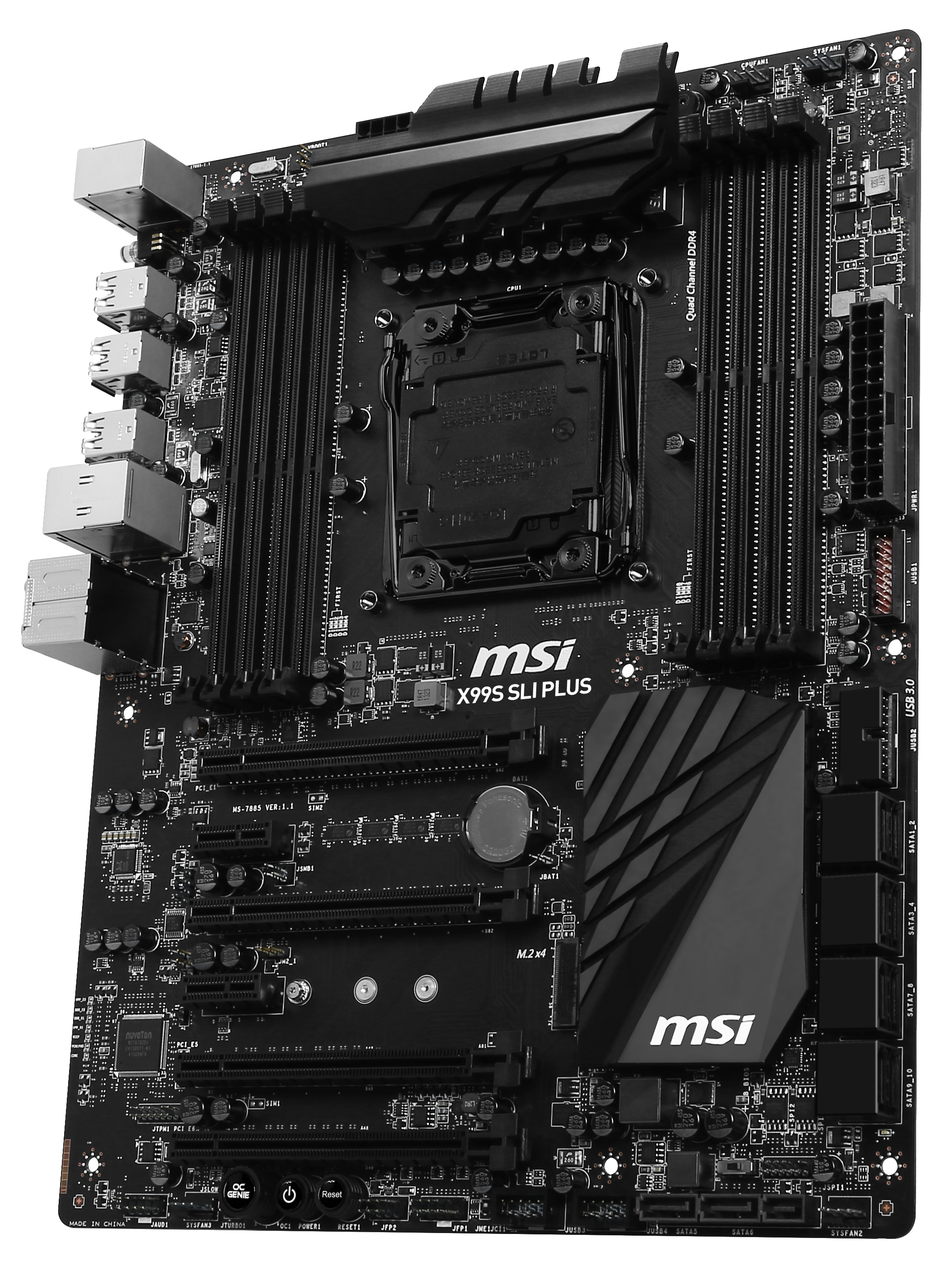
The PCIe layout of the motherboard is ultimately geared towards tri-GPU setups. I say this because in a dual GPU setup, the first two full-length PCIe slots are occupied rather than the first and third, which reduces the airflow between them. The PCIe slots are arranged such that:
40 PCIe 3.0 CPU: x16, x16/x16, x16/x16/x0/x8
28 PCIe 3.0 CPU: x16, x16/x8, x8/x8/x8/x0
This means that for the 5960X and 5930K, the third GPU must be in the bottom PCIe slot, whereas for the 5820K, the third GPU is in the third full-length PCIe slot.
I must offer MSI kudos as they have told me they should be including chipset diagrams in their manuals confirming where the bandwidth of the system goes:
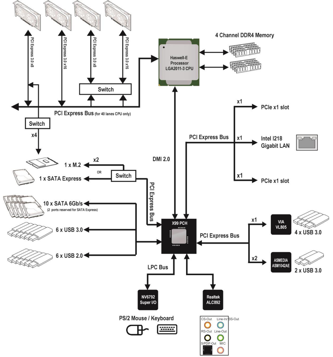
Note that next to the PCIe slots is the M.2 x4 connector which pulls lanes from what would be the final PCIe slot. This means that with a 40 PCIe lane CPU, a user has to choose between tri-GPU (x16/x16/x8) + M.2 x2 from the chipset, or 2x GPU (x16/x16) + M.2 x4. 5820K users will get M.2 x4 in any configuration (x16/x8, x8/x8/x8).
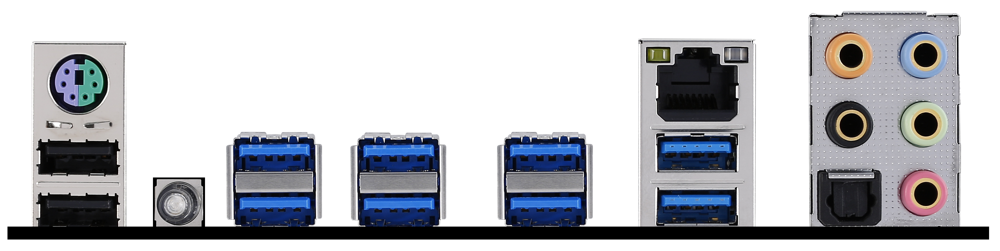
The rear panel is relatively empty, aside from eight of the USB 3.0 ports. We also get a combination PS/2 port, two USB 2.0 ports, a ClearCMOS button, the Intel network connection and gold-plated audio ports from the Realtek ALC892.
MSI X99S SLI Plus Board Features
| MSI X99S SLI Plus | |
| Price | US (Newegg) |
| Size | ATX |
| CPU Interface | LGA2011-3 |
| Chipset | Intel X99 |
| Memory Slots |
Eight DDR4 DIMM slots supporting up to 128 GB Up to Quad Channel, 2133-3333 MHz |
| Video Outputs | None |
| Network Connectivity | Intel I218-V |
| Onboard Audio | Realtek ALC892 |
| Expansion Slots |
4 x PCIe 3.0 x16 - 40 PCIe CPU: x16, x16/x16, x16/x16/-/x8 - 28 PCIe CPU: x16, x16/x8, x8/x8/x8/- 2 x PCIe 2.0 x1 |
| Onboard Storage |
6 x SATA 6 Gbps, RAID 0/1/5/10 4 x SATA 6 Gbps, no RAID 1 x SATA Express 1 x M.2 x4 / x2 |
| USB 3.0 |
6 x USB 3.0 via X99 (2 back panel, 2 headers) 2 x USB 3.0 via ASMedia ASM1042E Controller (back panel) 4 x USB 3.0 via VIA VL805 Controller (back panel) |
| Onboard |
10 x SATA 6 Gbps 1 x SATA Express 1 x M.2 2 x USB 3.0 headers 2 x USB 2.0 headers 5 x Fan headers 1 x TPM header Power/Reset Buttons OC Genie Button Multi BIOS Switch Front Panel Header Front Audio Header |
| Power Connectors |
1 x 24-pin ATX 1 x 8-pin CPU |
| Fan Headers |
2 x CPU (4-pin) 3 x SYS (4-pin) |
| IO Panel |
1 x PS/2 Combination Port 2 x USB 2.0 8 x USB 3.0 1 x Intel I218-V Network 1 x ClearCMOS Button Audio Jacks |
| Warranty Period | 3 Years |
| Product Page | Link |
For $230, X99 does not come with much extra. This is shown by the single network port, no WiFi, and the Realtek ALC892 codec which comes near bottom of the 7 channel audio codecs. MSI has bumped up the USB 3.0 ports to twelve however, using a regular ASMedia controller and a cheaper VIA controller.
MSI X99S SLI Plus BIOS
The basic outline of the MSI BIOS has not changed that much since the introduction of a graphical BIOS however its implementation has significantly improved. We do not get much more over MSI’s Z97 series - only those options related to X99 are added. The layout is such that a persistent top ribbon is present indicating the motherboard being used, the BIOS version, the CPU installed, the CPU frequency, the memory size, the memory speed and the system temperatures. There is perhaps some whitespace here for some fan speeds as well.
Note that we don’t have the XMP button similar to Z97. This is because when using a kit without an XMP profile, the button disappears. I would rather MSI still had the button present, but it was greyed out to indicate it was unavailable. I should add that MSI has perhaps missed a trick with the whole BIOS color scheme, as giving it a black aesthetic to match the motherboard would synchronize the user experience.
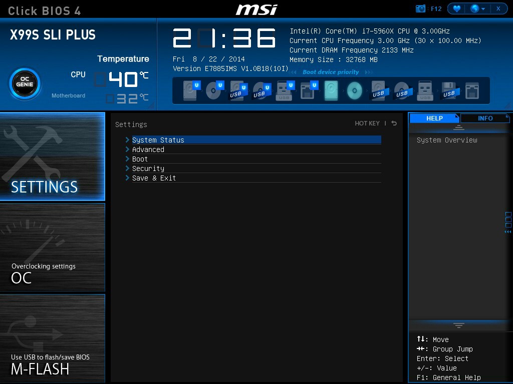
MSI’s system splits the BIOS up into two main areas – Settings and Overclocking. The Settings menu again subdivides into the System Status, Advanced, Boot, Security and Save & Exit.
For users wanting to adjust the PCIe bandwidth or disable the extra controllers, the Advanced menu gives all these options in separate sub-menus.
For example, in the PCIe Subsystem menu, the M.2 slot can be configured for both PCIe M.2 and SATA M.2 drives.
The Peripheral menu has the Hot Plug options for all the SATA ports. As with the other motherboards, the SATA ports are RAID capable but the sSATA are not, due to two AHCI controllers being present in the PCH with different functions. Unfortunately MSI does not distinguish here which are RAID capable and which are not – for reference SATA ports 1-6 allow RAID 0/1/5/10.
The other item of note in the Settings tab is that the user can issue a one-time boot override to a storage device of their choice:
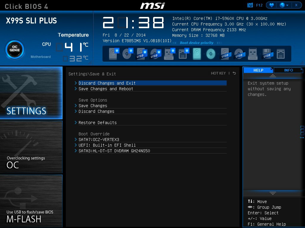
The OC Menu is almost identical to Z97, allowing both a simple mode and an advanced mode:
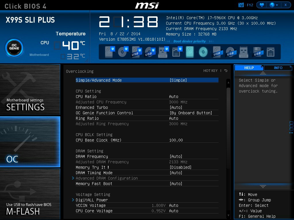
Thankfully MSI has decided to keep the new arrangement of overclocking options, starting with CPU/BCLK, DRAM, Voltage and then others:
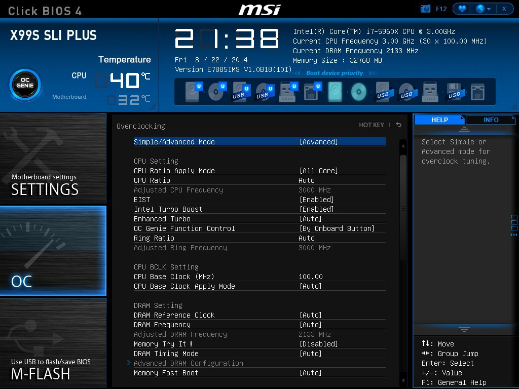
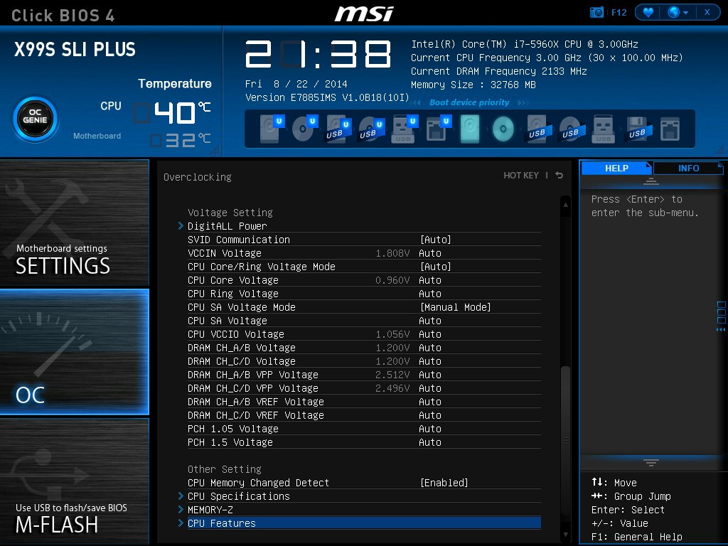
Advanced mode opens up a larger selection of options for experienced overclockers who are used to them. Users can also select when an enhanced BCLK overclock is applied (either before POST or after), and the Mem Try It option provides a couple of options for attempting to tighten up memory timings:
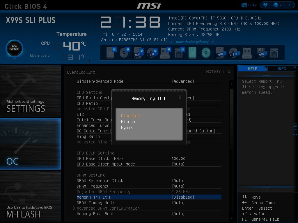
The DRAM options allow for control over the sub-timings, and it is good to see that the current timings are shown alongside the option to adjust them.
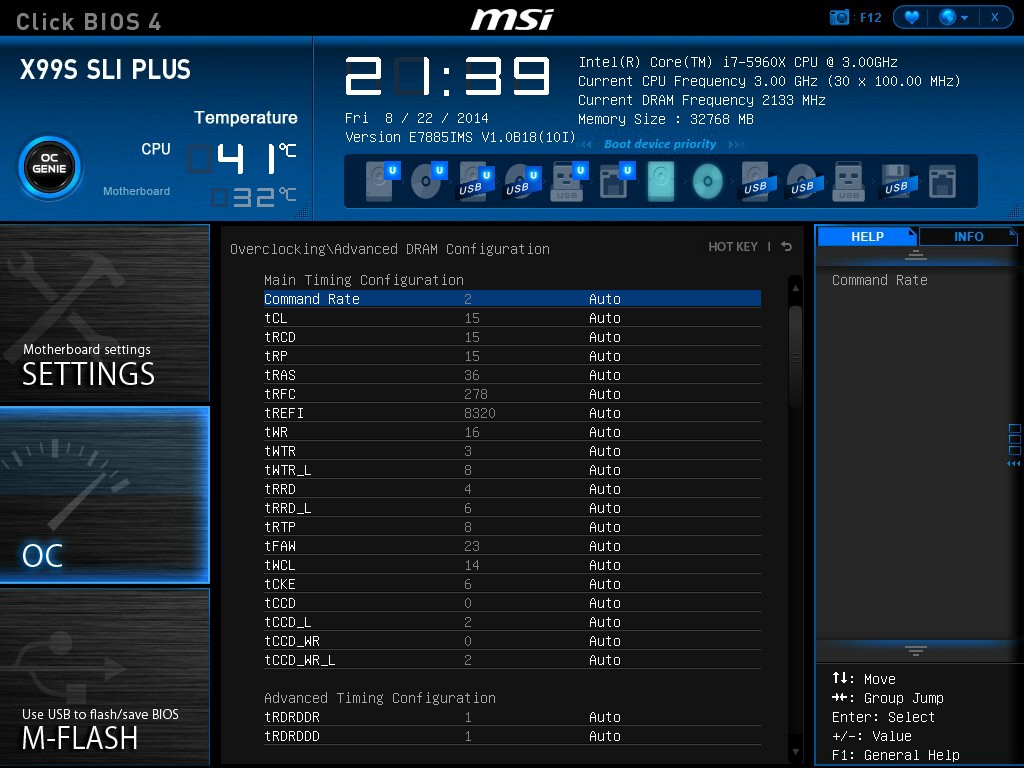
Unfortunately the Load Line Calibration issue with MSI motherboards rears its head again. Under the digital power menu, it gives an option for CPU VDroop Offset, and allows the user to set ‘Auto, +12.5% - 100%’, but does not inform the user which way around it should be for a constant voltage response. Other motherboard manufacturers have this option sorted by either providing a graph or renaming the options to ‘Auto, Low, Medium, High, Turbo, Extreme’. MSI could learn a trick or two in this instance.
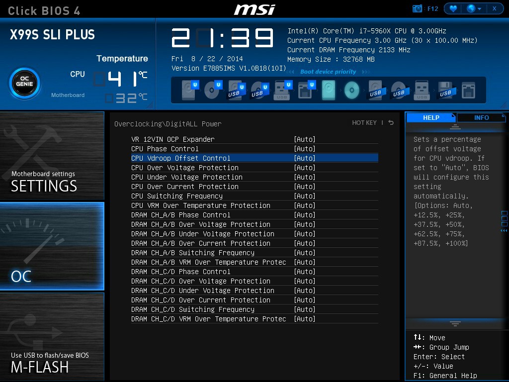
The OC menu also allows users to see the SPD information of the DRAM and adjust various aspects of the CPU features:
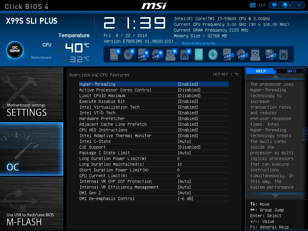
Alongside the Settings and OC tabs, the BIOS offers the M-Flash tool to update to the latest BIOS, overclocking profiles that can be saved and reloaded, a favorites menu for users to assign options they are used to (although not particularly needed with the new aligned OC menu) and also adjust the entry point of the BIOS.
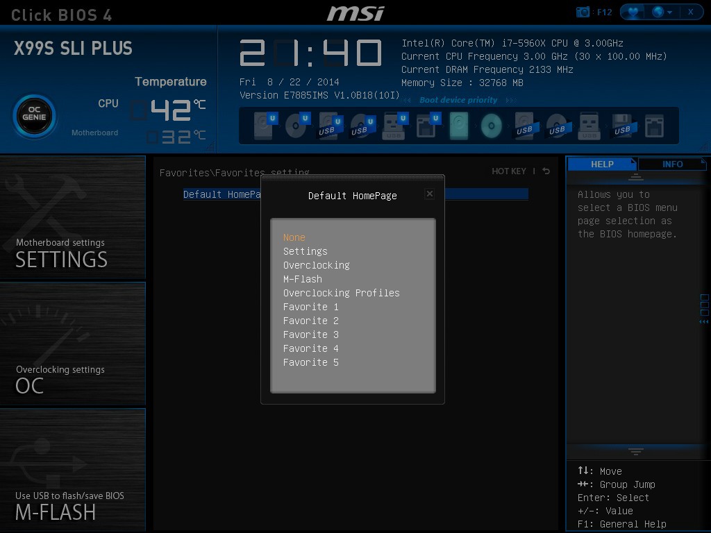
The Hardware Monitor tab gives the fan options, which in recent generations has been substantially upgraded to some of the best we have ever seen.
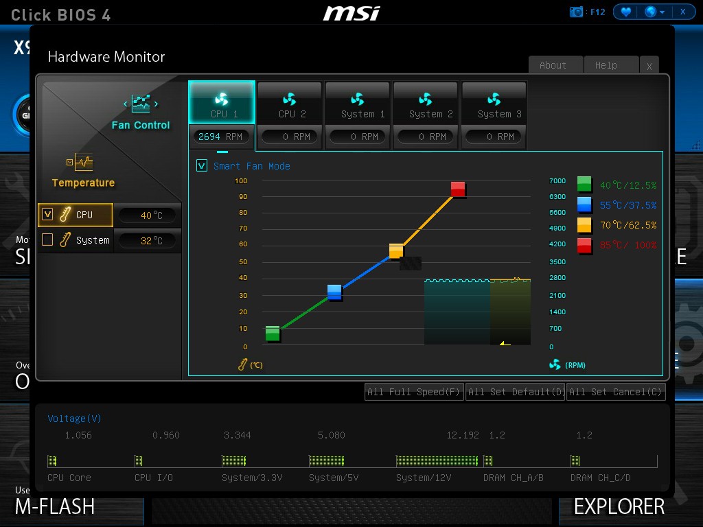
When the Graphical BIOS nomenclature was introduced, the ‘graphical’ part was designed to help the user experience and interactivity with what are normally mundane options. The fan controls are a perfect example – a user should be able to see a multipoint gradient graph and adjust it using the mouse, rather than fiddling with menu options. MSI’s graph adjustments are not as finely grained as some other manufacturers, but the user experience is right on the money:
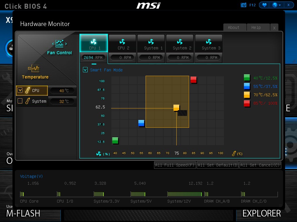
MSI now needs to introduce some internal testing functionality so that the system can test the fan and adjust the scale on the graph appropriately for the fan response.
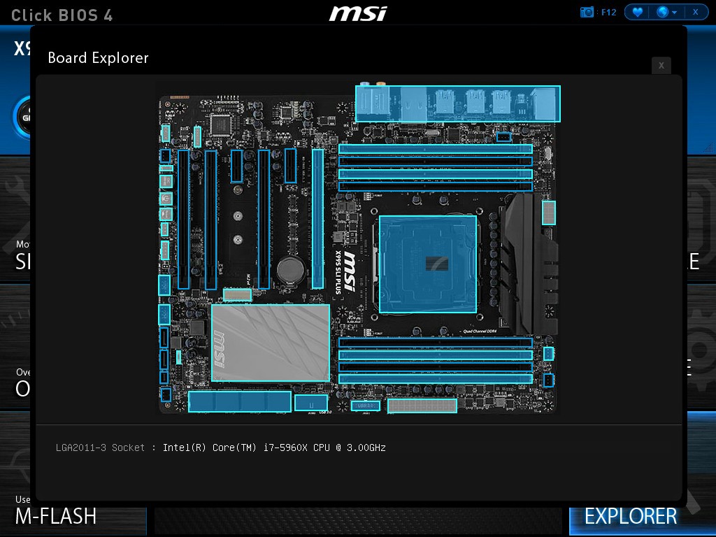
Similar to ASRock, we also get the Board Explorer functionality which allows the user to see what is installed. This is also useful if one stick of memory is not being seen or a PCIe device is not detected.


MSI X99S SLI Plus Software
Over the last couple of generations, MSI’s main hub of options has switched from a combination of Control Center and MSI Suite to Command Center with a much cleaner interface and array of options. The driver disk also offers some MSI branded wallpapers for installation along with the drivers and software:
I am always up for a change in background to align with the products I have purchased, and while I might suggest that MSI missed the mark by not adding an all-black SLI Plus type of background, anything beats the default Windows desktop I usually have to look at when testing.
One of MSI’s recent pushes in software has been with the ECO Center, designed to help users disable certain parts of the motherboard to save power.
It is not advised to disable the CPU fan unless it is powered with a fan controller elsewhere! Perhaps MSI should add that as a warning next to that option. However saving the odd watt here or there might make a small adjustment to anyone’s electricity bill. I normally work along the line of 1W = $1/yr at 12¢ per kWh as a rough guide when I am energy saving, although local pricing might vary (I actually pay £0.15/kWh here, or 24¢). Perhaps MSI should add a calculator in here to let users see what they are saving.
With the latest operating systems supporting UEFI fast booting methods, MSI has added an option to enable this feature along with a button to access the BIOS on the next reboot. Personally I find this a nice option to have, especially when overclock testing a new system – no more pressing DEL/F2 to get into the BIOS.
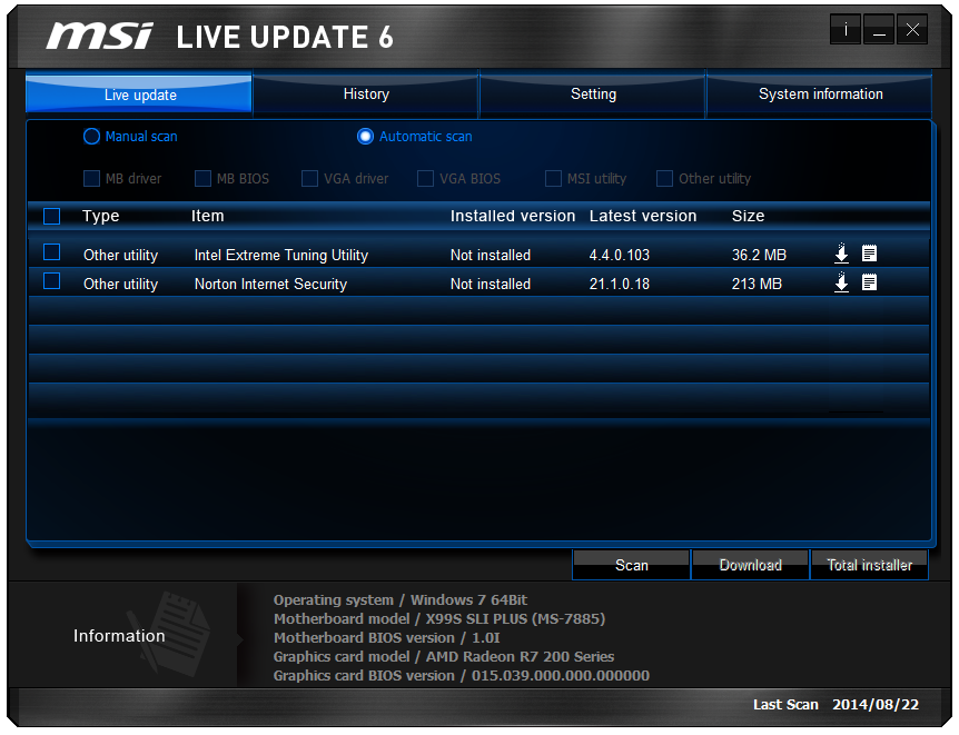
One of the cornerstones of the MSI software package is Live Update 6, which still holds the title as the best update package available on any motherboard. This downloads a list of what drivers/software should be on the motherboard and then compares it to what the user actually has. The ones that do not match are then offered as downloads, including sizes of download, and then the progress is shown as the updates are downloaded and installed. No other update package comes close, however there is one small issue. I would suggest to MSI to have an option to disable certain updates – I certainly do not want to download additional ‘Internet Security’ when I have my own preferred option on hand.
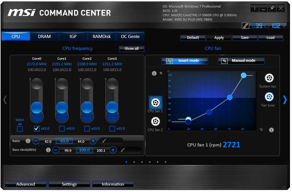
The Command Center software is where most of the regular action happens, with this front page showing which CPU is in use, what motherboard and BIOS version is in play and what operating system is installed. Here we also get quick access to CPU Multiplier and BCLK overclocks, as well as graphical CPU fan adjustment. The Fan Tune option allows the system to detect the fan power and speed response to help the user adjust the fans based on the dead zone in each.
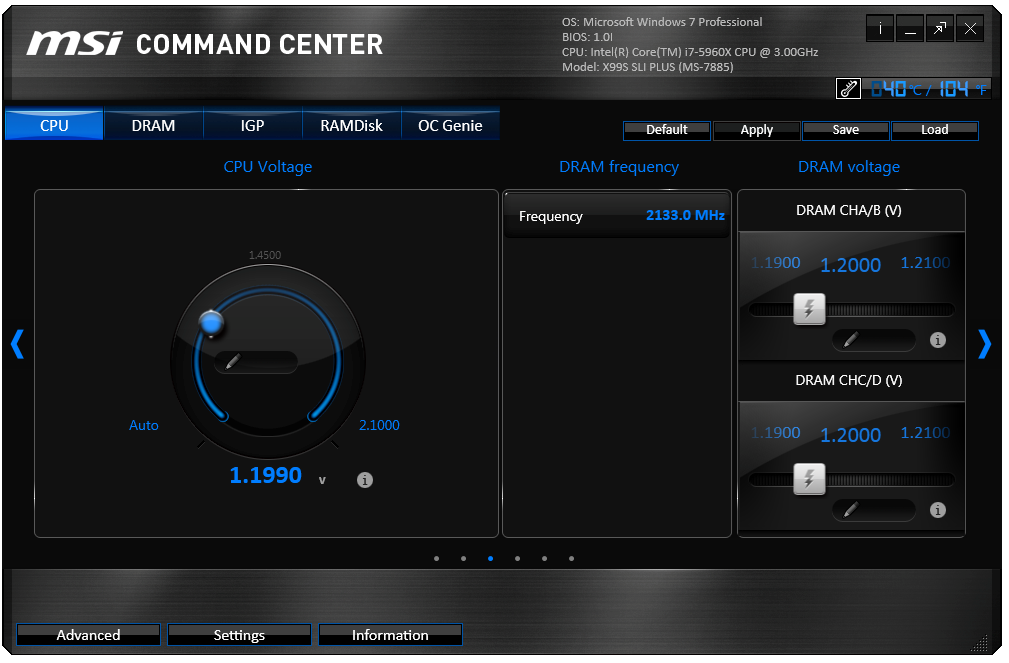
Unfortunately MSI has not fixed the error in Command Center I brought to their attention in the last generation – no user should be allowed the option to enable 2.1 volts to their processor. Not even extreme overclockers using liquid nitrogen will need (or can control) that much voltage, so it should not even be an option to regular users in the software without some big flashy warnings. Other manufacturers sometimes offer something similar, but they do not advertise 2.100 volts as the max on their sliders or dials, whereas for MSI it is staring the user right in the face. Come on MSI, step up the game and limit it to something more useful, such as +30% of stock voltage detected on the CPU.
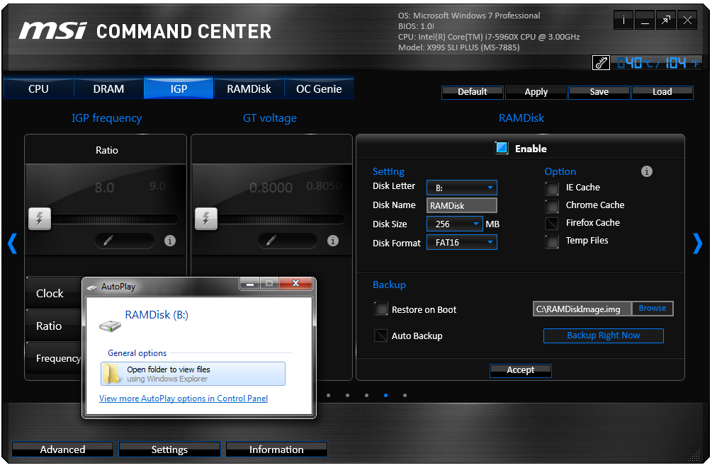
Command Center also allows a RAMDisk, although unlike ASRock’s implementation, the size of the RAMDisk is only limited by the drop down menu. Annoyingly the user has to enable the RAMDisk (which might take a minute) before re-enabling it with a new disk size other than 256 MB. This should be adjusted to improve the user experience.
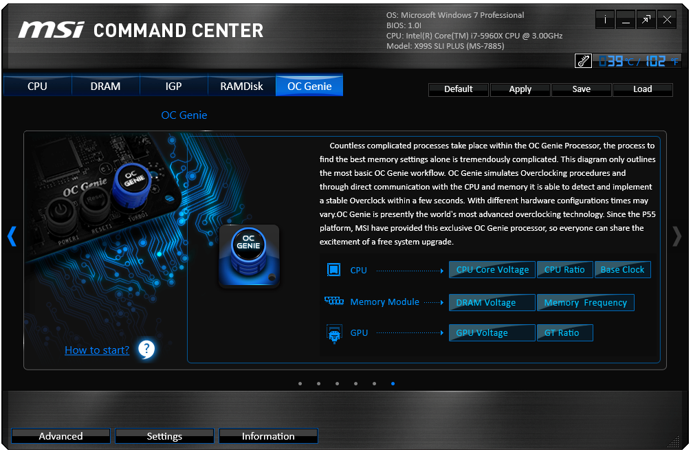
Enabling OC Genie can also be done in software if the button onboard is unavailable – either through Command Center here or via the BIOS.
Aside from the monitoring and information tabs also in Command Center, users can download and install two newer software packages aimed at extreme overclockers that cannot install extra fluff in order to squeeze the maximum performance out of their systems.
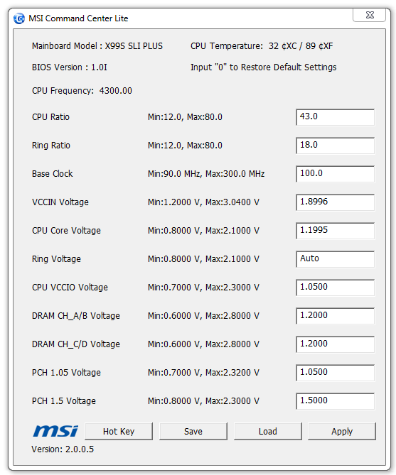
CC Lite is now on v2, suitable for X99 processors. Here adjusting the text and clicking Apply is all that is needed to enable an overclock. Users can also adjust the overclock with a selected hotkey, which is especially useful for benchmarks that have variable CPU load sections.
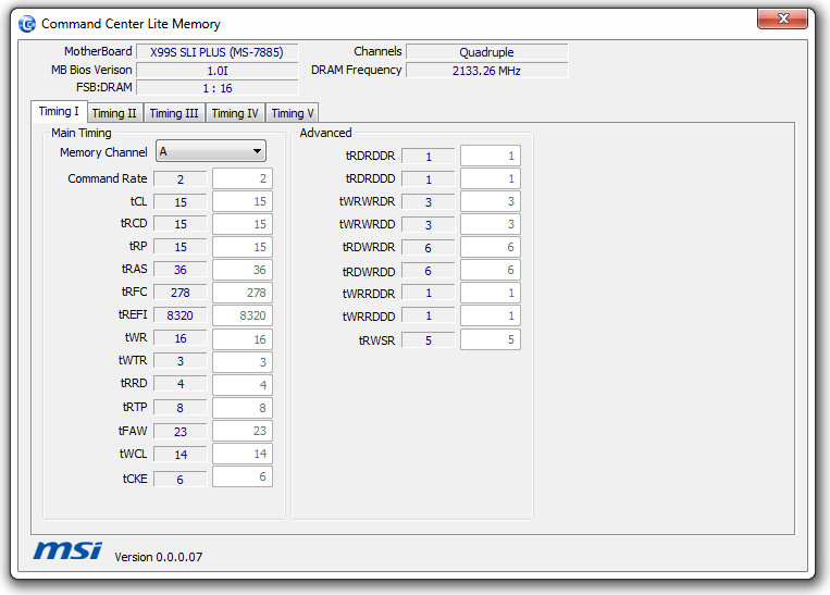
Newer to the Lite family is the CC Memory adjustment software, as shown by the version number 0.0.0.07. Similar in nature to CC Lite, the focus here is on the memory sub-timings.


Box Contents and What to Expect
Over the years of reviewing motherboards, it is clear that the price of the overall package is a good indicator of what is inside the box. The cheaper motherboards below $100 rarely come with more than a couple of SATA cables, whereas the most expensive $500 comes with external goodies, like the Rampage IV Black Edition with the included OC Panel. Motherboard manufacturers often have a choice – strip the goodies out to make the product hit a lower price point, or invest in the end-user having an experience with the product as long as the extras make sense.
With X99, almost all the motherboards are in the high end category because X99 itself is a premium product, so we expect to see more than just SATA cables here. One of the common features with the gaming motherboards will be addition of licenses for gaming related software such as XSplit or even bundled games for certain regions.
ASUS X99-Deluxe In The Box
Due to the X99-Deluxe price point around $400, as well as the extra features like the vertical M.2 and Hyper x4 M.2, we get a fair amount of stuff:
Driver Disk
Manuals
Quick Installation Guide
Rear IO Shield
Vertical M.2 Brace and clips
Hyper M.2 x4 PCIe card
Wi-Fi Antenna for 3T3R
Fan Extension Card with adhesive
Two-pin Thermistor
3-Way SLI Flexible Connector
8 SATA Cables
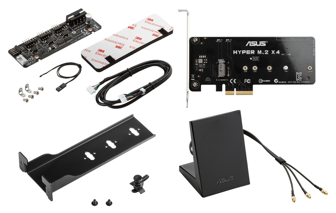
In the past, ASUS has added extras into the box where they were not ultimately necessary – this time each addition is required to make something already on the motherboard to work. ASUS is still hedging its bets between SATA Express and M.2 however, with the vertical M.2 required to get extra functionality out of the limited PCB space.
GIGABYTE X99-UD7 WiFi In The Box
At around $310, the UD7 is just below the ASRock X99 WS in price but sits quite nicely in the middle of the X99 range between the super-high end and the low end of the spectrum. At certain points in the past GIGABYTE has given the user a reduced level of box extras in order to drive the price point of a motherboard down into another category, but that might not be so much of an issue here.
In the box we get:
Driver Disk
Manual
Rear IO Shield with LED Lighting
Flexi 2-way SLI Bridge
Short 3-way SLI Bridge
Long 3-way SLI Bridge
4-way SLI Bridge
Flexi 2-way Crossfire Bridge
WiFi Antenna
1 to 3 ATX 12V power cable
Six Sleeved SATA Cables
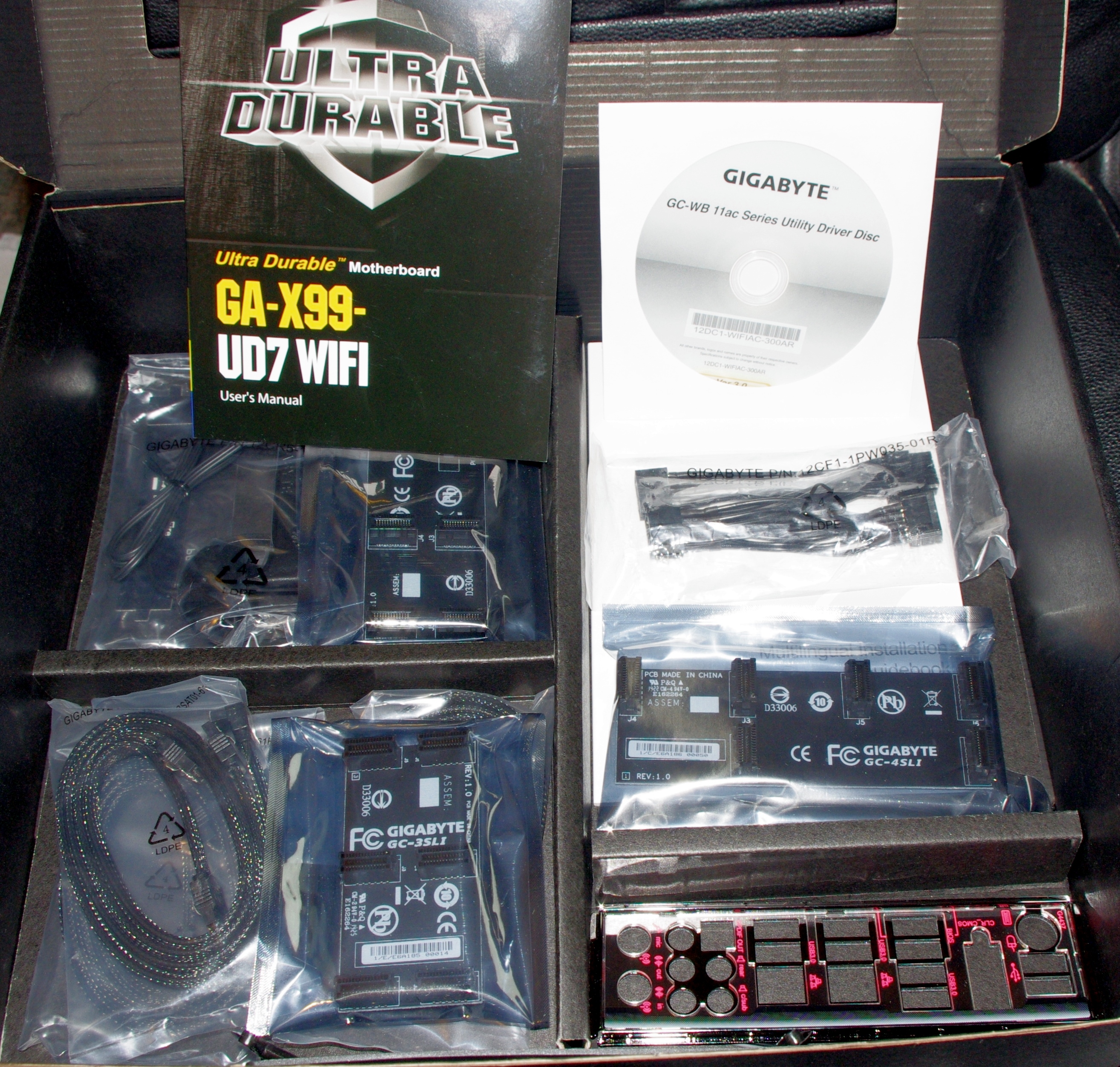
There is a healthy amount of SLI cables, including a long individual ones for three-way SLI with both 28 and 40 PCIe lanes CPUs. Adding the Crossfire bridge is a nice touch, as this seems to fly under everyone’s radar. Aside from the flashy IO shield and the antenna, one element stands out more than others: sleeved SATA cables!
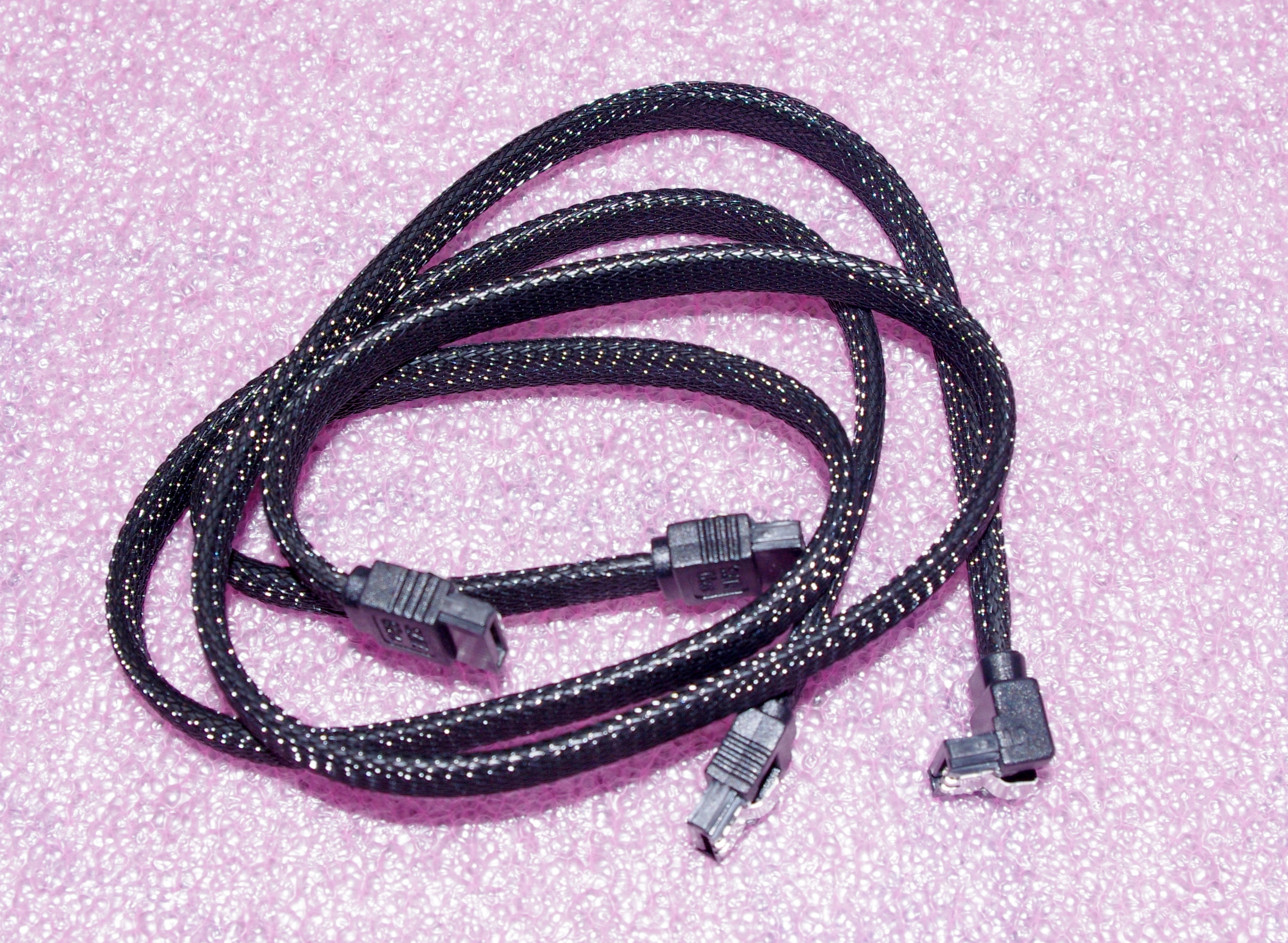
This needs to be a thing in all motherboard boxes today. Even if it costs an extra $0.50 per motherboard for six cables (because manufacturers buy in bulk) I would certainly give this the thumbs up.
ASRock X99 WS In The Box
In our previous consumer oriented WS motherboard reviews, these types of motherboards are filled with SATA cables and SLI bridges to support multiple NVIDIA cards for compute. Workstation users might also require other connections from the COM or LPT adapters, depending on their use, although the ASRock X99 WS eschews those here in favor of its own HDD Saver cable.
In the box we get:
Driver Disk
Rear IO Panel
Manual
HDD Saver Cable for two SATA devices
Four SATA Cables
2-slot, 3-slot and 4-slot SLI bridges
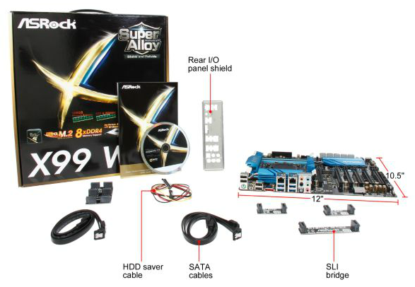
ASRock is often generous with SATA cables, and previous levels of box contents have gone above and beyond the expected price point. At $324 this box bundle represents almost a bare minimum, and I would have expected a couple more SATA cables at least.
MSI X99S SLI Plus In The Box
Being the cheapest motherboard of the ones tested today, we would hazard a guess and say that it would be coming with the least kit included. $230 is in the middle to mid-high range for Z97 motherboards and might come with an extra free thing or two, but $230 is almost bottom of the pile for X99 and will most likely be treated as such. In the box we get the following:
Driver Disk
Manual
Rear IO Shield
Flexi SLI Bridge
Six SATA Cables
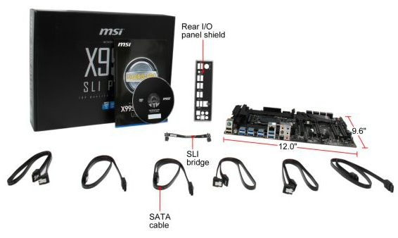
This is somewhat interesting. We have two more SATA cables than the ASRock motherboard, but it is odd that the X99S SLI Plus is designed around three-way GPU setups but we only get one SLI bridge in there. I would have assumed that users would be more interested in a three-way SLI Bridge than more SATA cables. However, because three-way SLI needs a strange way to connect them all, the extra cost of those cables might be prohibitive. Users will have to find SLI cables elsewhere for more than a 2-way graphics setup.
X99 Overclocking
With the move to Haswell-E, the X99 platform changes to a more Haswell-like approach. Due to the use of the FIVR (Fully Integrated Voltage Regulator) on the processor, the motherboard only has to deal with the VCIN to the CPU and then tell the CPU what to do with those voltages. This, theoretically, makes the motherboard manufacturer job much easier in terms of design, but could also make it tricky when it comes to differentiating itself from the competition.
Several points need mentioning here relating to motherboard design. If you skipped over our analysis of ASUS’ overclocking socket earlier in the review it is worth a read, as ASUS is using a different socket design to help extend the range of extreme overclocking, although this might not matter much for 24/7 overclocking.
Next is the power consumption, or more appropriately, the current draw. Haswell-E draws a lot of current through the EPS 12V connector (the 8-pin near the socket), with up to 25 amps with a decent overclock and beyond under more extreme cooling. As a result, a sufficient power supply is needed to do this – typically anything with an 80 PLUS rating should be fine, although it makes sense to check. Also there has been some backlash against motherboard manufacturers placing only one EPS 12V 8-pin connector on some motherboards, with a certain section of users suggesting that motherboards with two of these connectors will fare better with high end overclocks. While this may sound preferable, each EPS 12V connector is rated up to 36 amps, so the only danger comes from spiking when the power supply has insufficient over-current protection.
In our Haswell-E CPU review, we explained that Haswell-E acts much like Haswell when it comes to overclocking – if it takes only one bad core out of four to reduce maximum overclocks in an i7-4770K, then having eight cores in one CPU raises the chances that one core might be the limiting factor. Our two CPU results showed 4.6 GHz on the good processor and 4.3 GHz on the poor one, although ASUS’ overclocking guides suggest that 4.6 GHz at 1.3 volts is actually a good processor, whereas anything below 4.4 GHz is below average.
The i7-5960X is cool at stock and peak load due to the low turbo modes not requiring much extra voltage. Power consumption is relatively slow to raise as well, however above the 4.0 GHz mark, voltages, temperatures and power consumption all start to rise quickly. This means that most CPUs should handle 4.0 GHz with ease, giving a nice 33% overclock. Intel recommends a good air cooler or their TS13X liquid cooler as the bare minimum for the 140W TDP.
For our overclocking tests, we measure the automatic overclock features of each motherboard as well as our standard manual overclocking procedure.
Many thanks to...
We must thank the following companies for kindly providing hardware for our test bed:
Thank you to OCZ for providing us with PSUs and SSDs.
Thank you to G.Skill for providing us with memory.
Thank you to Corsair for providing us with an AX1200i PSU and a Corsair H80i CLC.
Thank you to MSI for providing us with the NVIDIA GTX 770 Lightning GPUs.
Thank you to Rosewill for providing us with PSUs and RK-9100 keyboards.
Thank you to ASRock for providing us with some IO testing kit.
Thank you to Cooler Master for providing us with Nepton 140XL CLCs.
Test Setup
| Test Setup | |
| Processor |
Intel Core i7-5960X ES 8 Cores, 16 Threads, 3.0 GHz (3.5 GHz Turbo) |
| Motherboards |
ASUS X99-Deluxe GIGABYTE X99-UD7 WIFI ASRock X99 WS MSI X99S SLI PLUS |
| Cooling |
Cooler Master Nepton 140XL Corsair H80i Thermalright TRUE Copper |
| Power Supply |
OCZ 1250W Gold ZX Series Corsair AX1200i Platinum PSU |
| Memory |
Corsair DDR4-2133 C15 4x8 GB 1.2V G.Skill Ripjaws 4 DDR4-2133 C15 4x8 GB 1.2V |
| Memory Settings | JEDEC @ 2133 |
| Video Cards | MSI GTX 770 Lightning 2GB (1150/1202 Boost) |
| Video Drivers | NVIDIA Drivers 332.21 |
| Hard Drive | OCZ Vertex 3 256GB |
| Optical Drive | LG GH22NS50 |
| Case | Open Test Bed |
| Operating System | Windows 7 64-bit SP1 |
| USB 2/3 Testing | OCZ Vertex 3 240GB with SATA->USB Adaptor |
| WiFi Testing | D-Link DIR-865L 802.11ac Dual Band Router |
Methodology:
For manual overclocks, based on the information gathered from previous testing, starts off at a nominal voltage and CPU multiplier, and the multiplier is increased until the stability tests are failed. The CPU voltage is increased gradually until the stability tests are passed, and the process repeated until the motherboard reduces the multiplier automatically (due to safety protocol) or the CPU temperature reaches a stupidly high level (100ºC+). Our test bed is not in a case, which should push overclocks higher with fresher (cooler) air.
ASUS X99-Deluxe
The X99-Deluxe has several modes of overclocking. The onboard TPU switch has two modes, one for multiplier only and the other for BCLK + Multiplier. The included software uses its 5-Way Optimization method to overclock the system, however it was not functional at the time of testing due to an error in our setup and our early sample.
Overall overclock performance of the ASUS X99-Deluxe comes top of the bunch, supporting 4.6 GHz within our absolute temperature window and 4.3 GHz very comfortably.
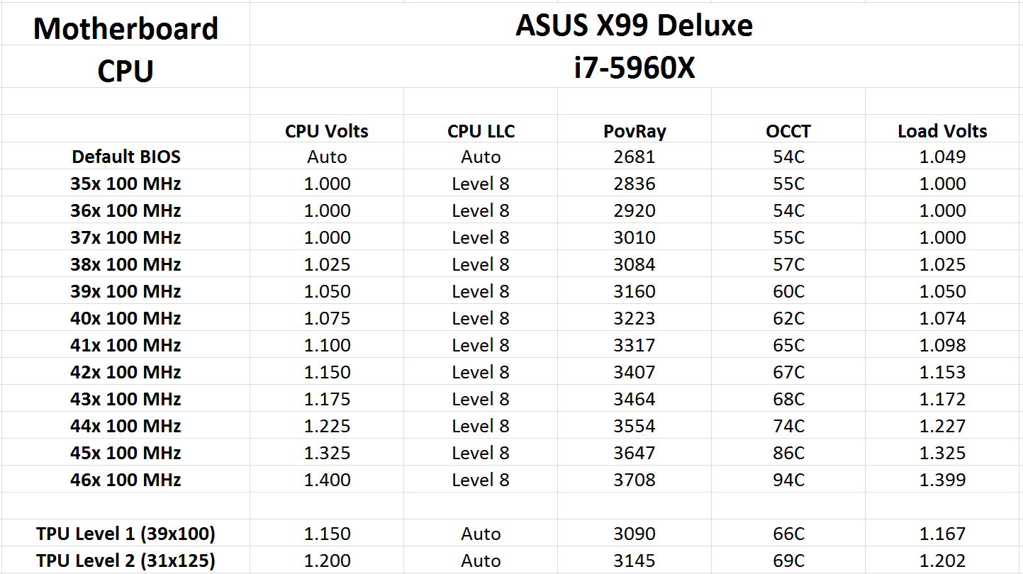
At 4.4 GHz we are still below 75C for our peak temperature readings and 4.3 GHz gives under 1.200 volts into the processor. It is hard to gauge if the OC socket is partially responsible for the ASUS scoring well compared to the rest.
GIGABYTE X99-UD7 WiFi
GIGABYTE loves its overclocking. Having something like the GIGABYTE OC Lab, manned by their in-house overclockers HiCookie and Sofos, shows that they are willing to dedicate time, money and resources in that direction. So while the UD7 is not the primary target for extreme overclocking, because it sits at the top of the Ultra Durable line it needs to have something there to help it perform. This is why we get things like voltage read points and buttons on board to help with rebooting.
GIGABYTE’s ecosystem around easy overclocks for most users is via the software, giving options from Light to Extreme with Auto Tuning in the mix. With our 5960X, these all gave reasonable results and voltages up to 4.1 GHz. When it came to manual overclocking, our sample gave a good correlation from voltage applied to voltage read, although our 75ºC peak was lower than expected at 4.2 GHz:

When the temperature gets too high, such as at 4.6 GHz and 1.350 volts, while the system is stable if we monitor the frequency it jumps below the 4.6 GHz mark on occasion. So at this point a non-voltage limited CPU in the UD7 ideally needs plenty of cooling.
ASRock X99 WS
While a Workstation class motherboard might not necessarily be geared towards overclocking in terms of OC-specific buttons or software, the nature of the components should be towards a higher stability, offering some amount of headroom for those versed in pushing frequency limits. The ASRock ecosystem offers a number of automatic overclock options in the BIOS and with the A-Tuning software, and the new layout in the BIOS for manual overclock settings, while easier to follow than before, does require a few more keypresses to go in and out of menus. Results from the ASRock are as follows:
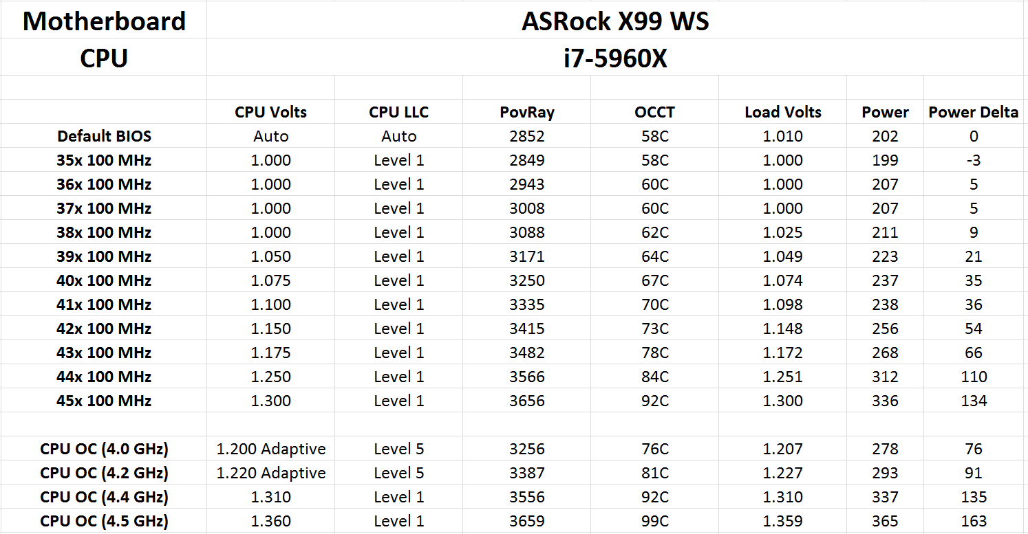
The automatic options are fairly aggressive with our average CPU sample, as given by the +0.060 volts at the 4.5 GHz level affording a power delta of +163W over stock. The 99ºC temperature is quite high as well, indicating that we are perhaps temperature limited overall. Note that if we draw a 75ºC line as a suitable peak temperature, none of the automatic settings fall under this, and it gives 4.2 GHz during manual testing.
MSI X99S SLI Plus
The X99S SLI Plus is not being marketed specifically as an overclocking oriented motherboard, although the press materials mention the OC engine to ease transitions from one CPU strap to another. The X99S SLI Plus is a motherboard designed to get up and go with a flick of the OC Genie button. Given the $230 nature of this board, it seems to be primarily aimed at i7-5820K users, however many of these will want to overclock as well. Our results are as follows:
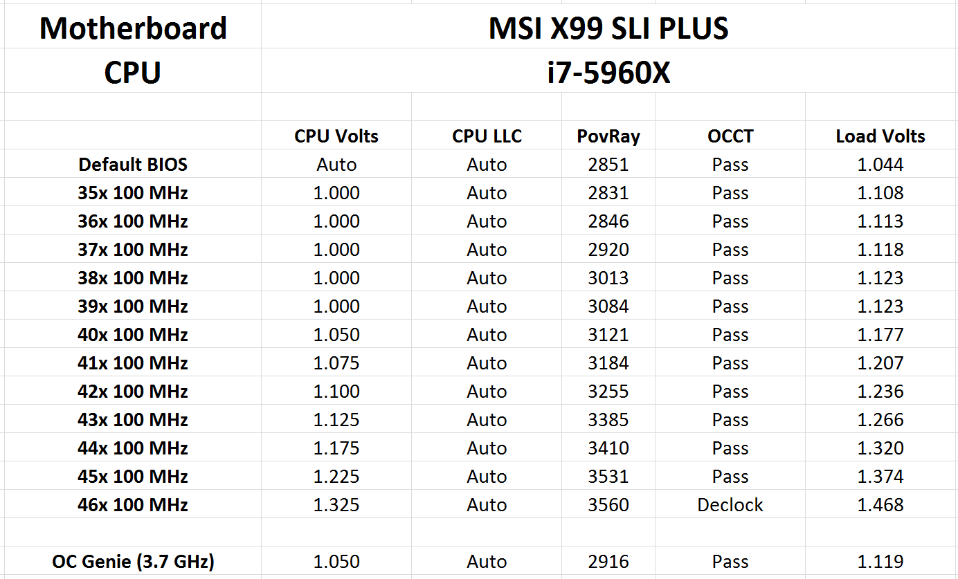
Several things are quite noteworthy. Firstly, the OC Genie setting is very mild. Every CPU under the sun should be managing 4.1 or 4.2 GHz, and MSI has played it safe going with 3.7 GHz.
Next up is the Load Line Calibration, which we had to leave on auto because the option in the BIOS after several generations still does not make it clear what it should be set as. Here there is a large disconnect between setting the CPU voltage and what the voltage reading is, to the point where at 4.5 GHz, 1.225 volts in the BIOS gives 1.374 volts at load – a +0.150 jump.
Finally, it comes to performance. When we put the overclocking results of the MSI up against any of the others, at each point the MSI result is behind:
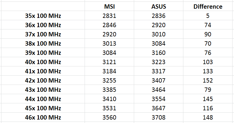
This is quite odd. It would seem the efficiency of the MSI motherboard when overclocked is somehow stunted to the point where the ASUS board at 4200 MHz can match the MSI at 4400 MHz. I am unsure if this can be fixed with a BIOS update, or if there is something fundamentally wrong with the MSI when overclocked, because its stock performance is actually rather good.
System Benchmarks
Power Consumption
Power consumption was tested on the system while in a single MSI GTX 770 Lightning GPU configuration with a wall meter connected to the OCZ 1250W power supply. This power supply is Gold rated, and as I am in the UK on a 230-240 V supply, leads to ~75% efficiency > 50W, and 90%+ efficiency at 250W, suitable for both idle and multi-GPU loading. This method of power reading allows us to compare the power management of the UEFI and the board to supply components with power under load, and includes typical PSU losses due to efficiency. These are the real world values that consumers may expect from a typical system (minus the monitor) using this motherboard.
While this method for power measurement may not be ideal, and you feel these numbers are not representative due to the high wattage power supply being used (we use the same PSU to remain consistent over a series of reviews, and the fact that some boards on our test bed get tested with three or four high powered GPUs), the important point to take away is the relationship between the numbers. These boards are all under the same conditions, and thus the differences between them should be easy to spot.
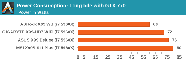
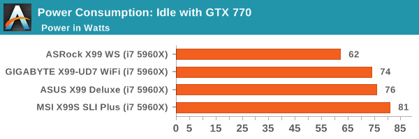
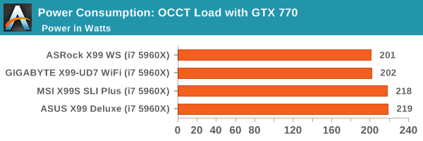
The ASRock leads the way in power consumption across the board, although the GIGABYTE has the smallest idle-to-peak delta. It will be interesting to see if this 20W window during our OCCT tests is prevalent among other X99 motherboards.
Windows 7 POST Time
Different motherboards have different POST sequences before an operating system is initialized. A lot of this is dependent on the board itself, and POST boot time is determined by the controllers on board (and the sequence of how those extras are organized). As part of our testing, we look at the POST Boot Time using a stopwatch. This is the time from pressing the ON button on the computer to when Windows 7 starts loading. (We discount Windows loading as it is highly variable given Windows specific features.)
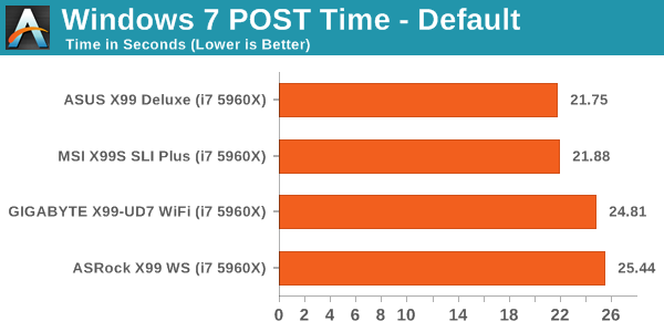
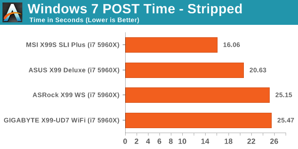
The new X99 POST sequence involves a fair amount of DRAM training (testing and verifying speeds) which adds an abnormal amount of time to the POST sequence. This is why every motherboard at default scores above 21 seconds. Not only this, but most of these BIOSes are not fully optimized in order to save time. X99 launch was rushed due to Intel, so it might be the case that we see faster times later on in the life cycle of the platform.
Rightmark Audio Analyzer 6.2.5
Rightmark:AA indicates how well the sound system is built and isolated from electrical interference (either internally or externally). For this test we connect the Line Out to the Line In using a short six inch 3.5mm to 3.5mm high-quality jack, turn the OS speaker volume to 100%, and run the Rightmark default test suite at 192 kHz, 24-bit. The OS is tuned to 192 kHz/24-bit input and output, and the Line-In volume is adjusted until we have the best RMAA value in the mini-pretest. We look specifically at the Dynamic Range of the audio codec used on board, as well as the Total Harmonic Distortion + Noise.
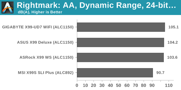
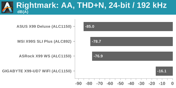
The ASUS takes the lead in THD+N by a long way, and the differences between the ALC1150s and the ALC892 in the MSI show up in the Dynamic Range tests. Unfortunately the GIGABYTE had an issue with its test, causing high levels of software-detectable distortion at high volume levels.
USB Backup
For this benchmark, we transfer a set size of files from the SSD to the USB drive using DiskBench, which monitors the time taken to transfer. The files transferred are a 1.52 GB set of 2867 files across 320 folders – 95% of these files are small typical website files, and the rest (90% of the size) are small 30 second HD videos. In an update to pre-Z87 testing, we also run MaxCPU to load up one of the threads during the test which improves general performance up to 15% by causing all the internal pathways to run at full speed.
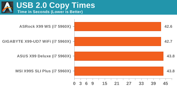
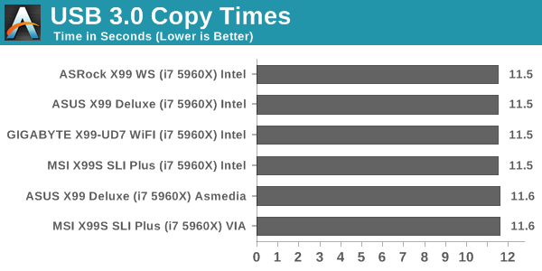
DPC Latency
Deferred Procedure Call latency is a way in which Windows handles interrupt servicing. In order to wait for a processor to acknowledge the request, the system will queue all interrupt requests by priority. Critical interrupts will be handled as soon as possible, whereas lesser priority requests such as audio will be further down the line. If the audio device requires data, it will have to wait until the request is processed before the buffer is filled.
If the device drivers of higher priority components in a system are poorly implemented, this can cause delays in request scheduling and process time. This can lead to an empty audio buffer and characteristic audible pauses, pops and clicks. The DPC latency checker measures how much time is taken processing DPCs from driver invocation. The lower the value will result in better audio transfer at smaller buffer sizes. Results are measured in microseconds.
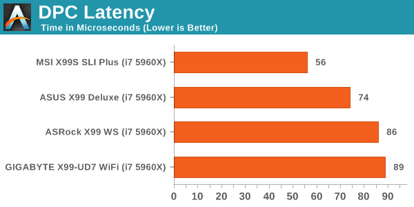
DPC for X99 is quite impressive all around, with every motherboard scoring under 100 microseconds.
CPU Benchmarks
Readers of our motherboard review section will have noted the trend in modern motherboards to implement a form of MultiCore Enhancement / Acceleration / Turbo (read our report here) on their motherboards. This does several things, including better benchmark results at stock settings (not entirely needed if overclocking is an end-user goal) at the expense of heat and temperature. It also gives in essence an automatic overclock which may be against what the user wants. Our testing methodology is ‘out-of-the-box’, with the latest public BIOS installed and XMP enabled, and thus subject to the whims of this feature. It is ultimately up to the motherboard manufacturer to take this risk – and manufacturers taking risks in the setup is something they do on every product (think C-state settings, USB priority, DPC Latency / monitoring priority, memory subtimings at JEDEC). Processor speed change is part of that risk, and ultimately if no overclocking is planned, some motherboards will affect how fast that shiny new processor goes and can be an important factor in the system build.
For our tests today, it would seem that all the motherboards had some form of MultiCore Turbo, although because we are testing with a JEDEC memory kit, some are more ‘turned on’ than others. The GIGABYTE and ASUS motherboards seemed more content at stock and mid-turbo frequencies, whereas the MSI and ASRock were more aggressive.
Point Calculations – 3D Movement Algorithm Test: link
3DPM is a self-penned benchmark, taking basic 3D movement algorithms used in Brownian Motion simulations and testing them for speed. High floating point performance, MHz and IPC wins in the single thread version, whereas the multithread version has to handle the threads and loves more cores.
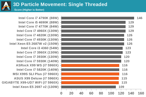
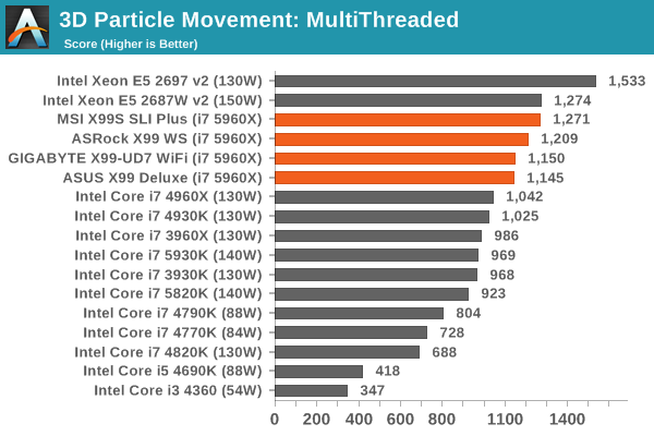
The MSI takes a commanding lead in the multi-threaded version of the test.
Compression – WinRAR 5.0.1: link
Our WinRAR test from 2013 is updated to the latest version of WinRAR at the start of 2014. We compress a set of 2867 files across 320 folders totaling 1.52 GB in size – 95% of these files are small typical website files, and the rest (90% of the size) are small 30 second 720p videos.
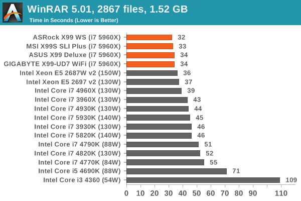
In comparison, the ASRock wins here.
Image Manipulation – FastStone Image Viewer 4.9: link
Similarly to WinRAR, the FastStone test us updated for 2014 to the latest version. FastStone is the program I use to perform quick or bulk actions on images, such as resizing, adjusting for color and cropping. In our test we take a series of 170 images in various sizes and formats and convert them all into 640x480 .gif files, maintaining the aspect ratio. FastStone does not use multithreading for this test, and thus single threaded performance is often the winner.
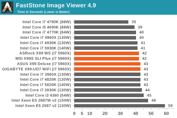
The split between MSI/ASRock against ASUS/GIGABYTE results in a one second gap in our FastStone test.
Video Conversion – Handbrake v0.9.9: link
Handbrake is a media conversion tool that was initially designed to help DVD ISOs and Video CDs into more common video formats. The principle today is still the same, primarily as an output for H.264 + AAC/MP3 audio within an MKV container. In our test we use the same videos as in the Xilisoft test, and results are given in frames per second.
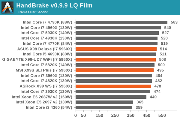
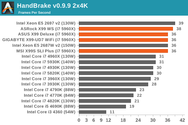
Interestingly here the ASUS and GIGABYTE pull ahead during the low quality test, but at 4K the ASRock scores the points.
Rendering – PovRay 3.7: link
The Persistence of Vision RayTracer, or PovRay, is a freeware package for as the name suggests, ray tracing. It is a pure renderer, rather than modeling software, but the latest beta version contains a handy benchmark for stressing all processing threads on a platform. We have been using this test in motherboard reviews to test memory stability at various CPU speeds to good effect – if it passes the test, the IMC in the CPU is stable for a given CPU speed. As a CPU test, it runs for approximately 2-3 minutes on high end platforms.
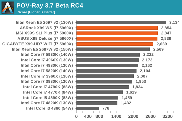
MultiCore Turbo affects motherboards more in tests such as POV-Ray, and the GIGABYTE drops down here.
Synthetic – 7-Zip 9.2: link
As an open source compression tool, 7-Zip is a popular tool for making sets of files easier to handle and transfer. The software offers up its own benchmark, to which we report the result.
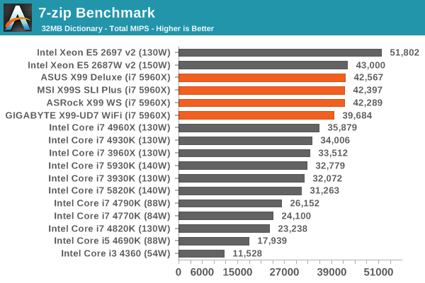
Gaming Benchmarks
F1 2013
First up is F1 2013 by Codemasters. I am a big Formula 1 fan in my spare time, and nothing makes me happier than carving up the field in a Caterham, waving to the Red Bulls as I drive by (because I play on easy and take shortcuts). F1 2013 uses the EGO Engine, and like other Codemasters games ends up being very playable on old hardware quite easily. In order to beef up the benchmark a bit, we devised the following scenario for the benchmark mode: one lap of Spa-Francorchamps in the heavy wet, the benchmark follows Jenson Button in the McLaren who starts on the grid in 22nd place, with the field made up of 11 Williams cars, 5 Marussia and 5 Caterham in that order. This puts emphasis on the CPU to handle the AI in the wet, and allows for a good amount of overtaking during the automated benchmark. We test at 1920x1080 on Ultra graphical settings.

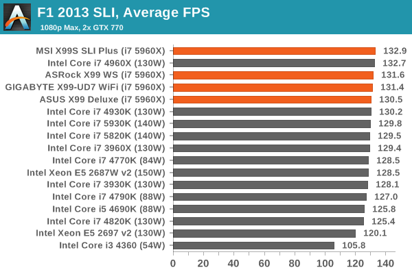
Bioshock Infinite
Bioshock Infinite was Zero Punctuation’s Game of the Year for 2013, uses the Unreal Engine 3, and is designed to scale with both cores and graphical prowess. We test the benchmark using the Adrenaline benchmark tool and the Xtreme (1920x1080, Maximum) performance setting, noting down the average frame rates and the minimum frame rates.

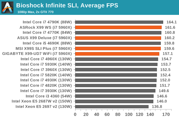
Tomb Raider
The next benchmark in our test is Tomb Raider. Tomb Raider is an AMD optimized game, lauded for its use of TressFX creating dynamic hair to increase the immersion in game. Tomb Raider uses a modified version of the Crystal Engine, and enjoys raw horsepower. We test the benchmark using the Adrenaline benchmark tool and the Xtreme (1920x1080, Maximum) performance setting, noting down the average frame rates and the minimum frame rates.

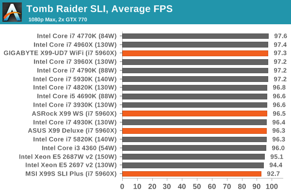
Sleeping Dogs
Sleeping Dogs is a benchmarking wet dream – a highly complex benchmark that can bring the toughest setup and high resolutions down into single figures. Having an extreme SSAO setting can do that, but at the right settings Sleeping Dogs is highly playable and enjoyable. We run the basic benchmark program laid out in the Adrenaline benchmark tool, and the Xtreme (1920x1080, Maximum) performance setting, noting down the average frame rates and the minimum frame rates.

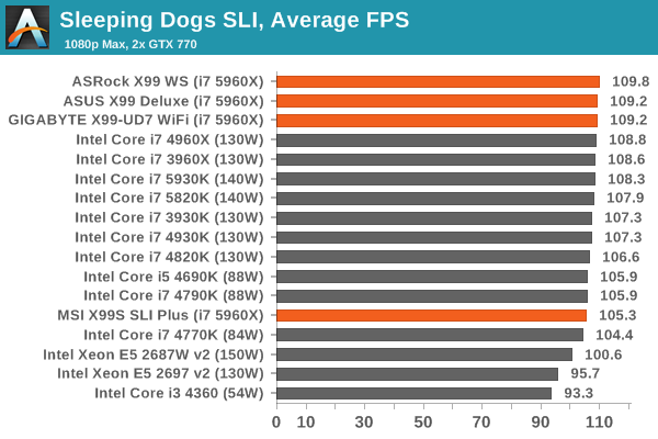
Battlefield 4
The EA/DICE series that has taken countless hours of my life away is back for another iteration, using the Frostbite 3 engine. AMD is also piling its resources into BF4 with the new Mantle API for developers, designed to cut the time required for the CPU to dispatch commands to the graphical sub-system. For our test we use the in-game benchmarking tools and record the frame time for the first ~70 seconds of the Tashgar single player mission, which is an on-rails generation of and rendering of objects and textures. We test at 1920x1080 at Ultra settings.

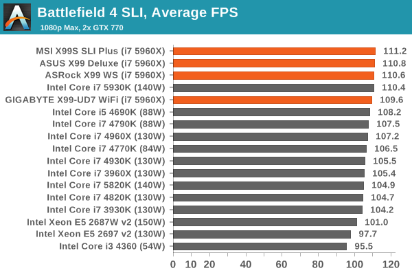
ASUS X99-Deluxe Conclusion
A lot of positive remarks have been made about the styling of the X99-Deluxe. There has been no modern attempt to style white and black properly on the motherboard, and when taking the product out of the packaging it does feel like there is a touch of finesse to the product. This may be derived purely from the white strip down the left hand side covering some of the PCB and the rear panel and the consistency in the visual aesthetic. On closer inspection, it does come to realize that the white strip is plastic and only there for the aesthetic value, but to ASUS’ credit it does look smooth and proud.
The X99-Deluxe is the most expensive X99 motherboard in our first set of reviews at $400, and actually sits near the top of the entire X99 stack. As a result, it has new or exciting features coming out of every corner. We discussed the new features such as the OC Socket to help with overclocking, the vertical M.2 x4 slot for drives and the multi-GPU switch that lights up the PCIe slots where GPUs should be placed for 2/3-way gaming. Also included in the box are a Hyper M.2 x4 PCIe card for more storage and an antenna for the 3T3R 802.11ac module – the X99-Deluxe is currently the only motherboard with a tri-stream 802.11ac solution integrated into the platform.
The more usual bonus features include dual SATA Express ports, dual Intel network connections and Crystal Sound 2 which translates as an improved ALC1150 codec with EMI shields, de-pop circuits, PCB separation and impedance detection. ASUS has also introduced a fan extension PCB, supporting another three four-pin headers alongside the six already on the motherboard. This comes with an adhesive strip, allowing system designers to place the fan PCB near where it is needed. All the fans are DC and PWM controllable as well.
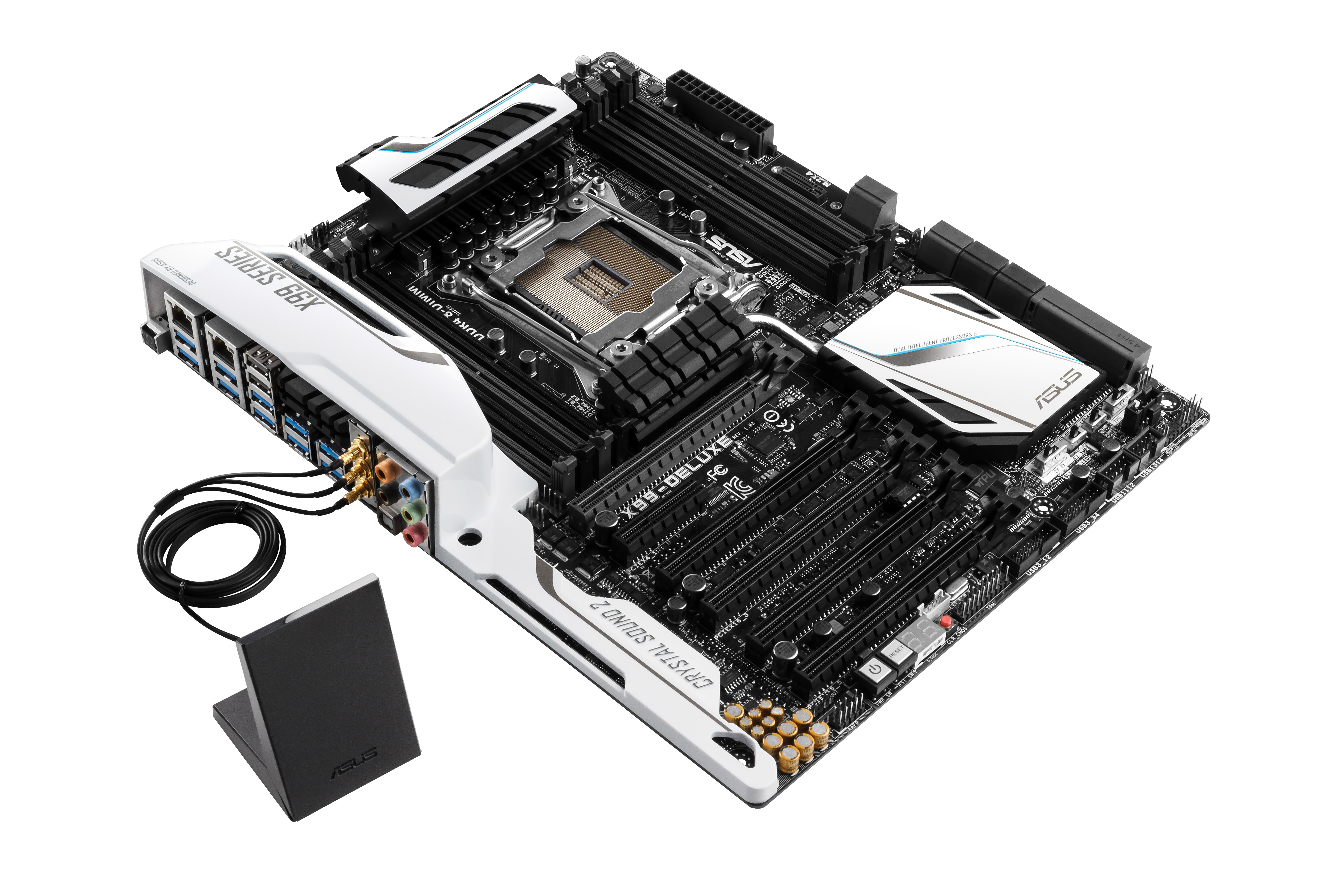
The performance of the ASUS X99-Deluxe is a little mixed. Overclocking results give it 4.6 GHz under 95C load temperatures, and audio results put it at the top of our X99 charts. DPC Latency is in the middle but still very good, with POST times around the 21 second mark similar to the other motherboards. Power consumption is also in the middle.
Unfortunately though the CPU performance at stock seems a little down compared to the others. We have tackled the issue of MultiCore Turbo previously at AnandTech, and the i7-5960X is odd that while it has a base frequency of 3.0 GHz, the 3.5 GHz turbo mode is quite rare and the CPU sits more happily at 3.3 GHz. It would seem that the ASUS X99-Deluxe does implement a form of MultiCore Turbo, although slightly less aggressive than some of the other motherboards. As a result, CPU performance at stock is a little down (1145 in 3DPM-MT vs 1271 for MSI). But, when overclocked, the ASUS seems to perform better than other motherboards (PovRay at 4.0 GHz, ASUS 3223 vs MSI 3121) so it does not come across as big worry – just place the system in TPU mode one and away you go.
It is easy to be impressed with the ASUS X99-Deluxe. Not only the design, but the BIOS, software and extra features all give it a boost above most of the X99 products on the market right now. Simple things like the XMP switch and the multi-GPU light-up LEDs improve the experience, while the bundled Hyper M.2 x4 PCIe card and 802.11ac 3T3R WiFi module give tangible benefits to spending over the average.
For the X99 launch, ASUS launched only two models to the North American market – this X99 Deluxe and the $500 Rampage V Extreme. The X99-A, X99-Pro and X99-WS are all in the pipeline, but it still means ASUS is focusing more on fewer motherboards giving time to improve each one. The argument from other manufacturers is that having more motherboards offers more choice, although if you want something like the X99-Deluxe, it is a polished product and hits the market it needs to with a wake-up call.
I enjoyed the X99-Deluxe. Most X99 users will too. Out of the motherboards tested today, it certainly deserves to be recommended for an i7-5960X build.

ASUS X99-Deluxe
GIGABYTE X99-UD7 WiFi Conclusion
GIGABYTE and ASUS are locked in a battle with each other to sell the most motherboards this year. Despite a few recent quarters of lower sales, the upswing in the gaming PC market driven by high resolution gaming and renewed interest sees both manufacturers aiming well above 20 million units each, despite a global motherboard sales number about 75-80 million expected for 2014. Each of these companies has a different tactic – ASUS goes for fewer SKUs and focuses on each one, whereas GIGABYTE offers more SKUs to appeal to more users. There are certain challenges in both lineups, and it reflects in the fact that ASUS had two motherboards at the launch of X99 and GIGABYTE aimed at eight.
The X99 UD7-WiFi sits at the top of GIGABYTE’s Ultra Durable line at $310, followed by the similar UD5, then UD4 and UD3. For overclocking there is the X99-SOC Force (and SOC Force-LN2 for extreme overclockers) with gaming relying on the Gaming 5, the Gaming 7 and the Gaming G1. This encompasses a price range from $245 (UD3) to $350 (SOC Force), so while we are aiming at the cheaper end of X99, the more $400 oriented products might be further down the line.
For the X99-UD7 WiFi, GIGABYTE certainly did a number of things right. Supplying WiFi via M.2 is a nice touch, giving a new way to introduce WiFi and then stacking another M.2 for storage on top. By placing the extra circuitry needed, GIGABYTE also ensures that every motherboard across its range can support full-bandwidth four-way GPU configurations. Things like the 30 micron gold pins and extra space for mounting holes also helps reduce issues from screwdrivers that stray or corrosion oriented climates.
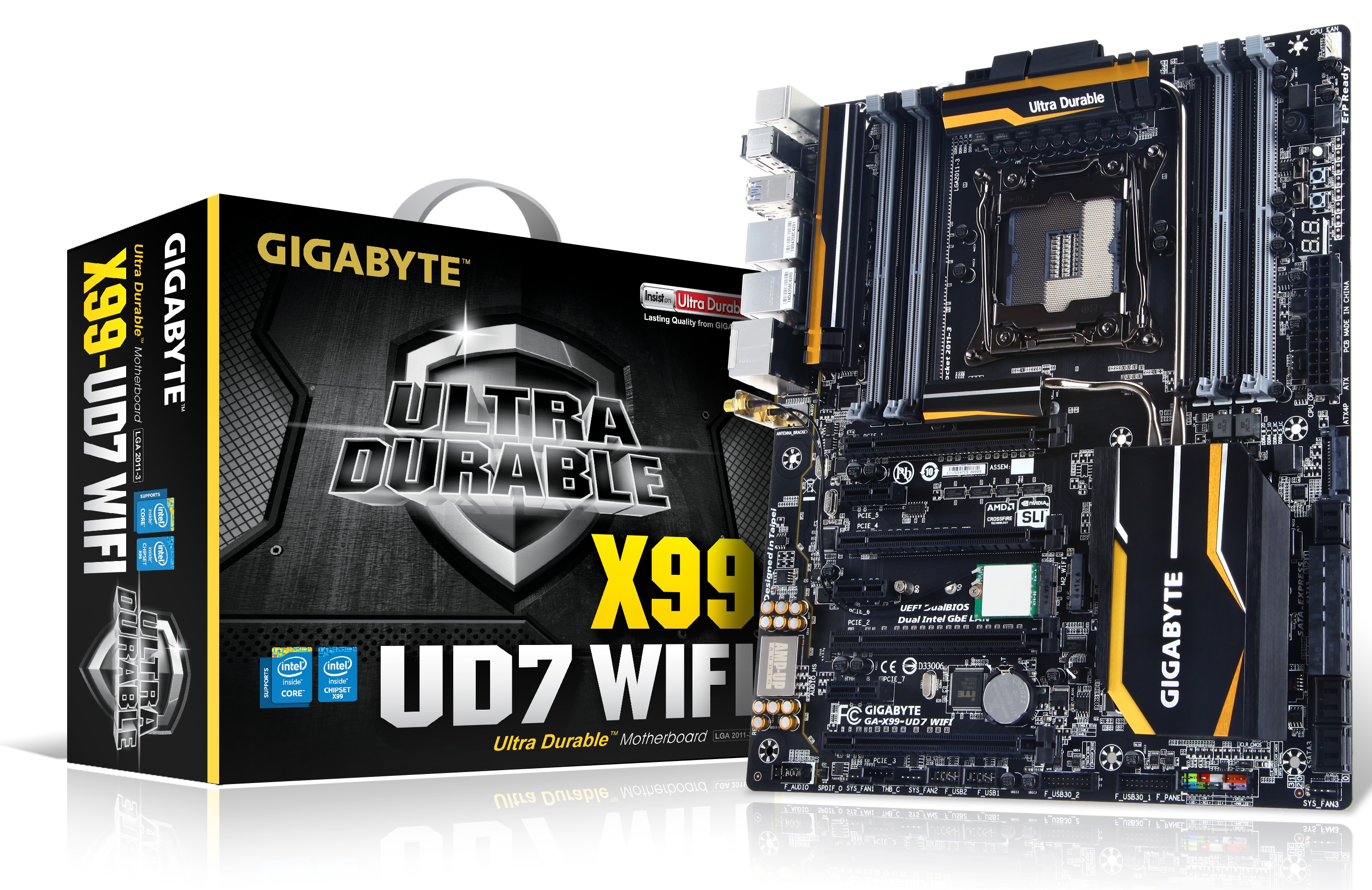
Despite all this, my biggest WOW moment with the GIGABYTE X99-UD7 WiFi was the bundled sleeved cables. Perhaps I spend too much time indoors reviewing CPUs and motherboards, but it is a nice touch that needs to be commonplace across all $150 and up motherboards. A positive about the PCIe area is the VGA power being provided by a SATA cable in the right area. The USB 3.0 layout is also good, giving two PCH headers and two Renesas hubs for eight ports on the rear to free up PCIe lanes.
There are some issues to take with the design, such as PCIe storage still being an issue depending on which route you take meaning that only one type can be used. While M.2 WiFi is a cool idea, and our sample had the WiFi antenna kept close to the motherboard by a plastic tool, it is not always wise to have those cables about on the motherboard.
On the benchmark front, the GIGABYTE suffers a little similar to the ASUS by not implementing a totally aggressive MultiCore Turbo throughout any hardware setup. So at stock we had a few numbers lower than expected, although when overclocked this no longer mattered so much. Peak power consumption under load was very good, along with USB speeds, although there was an issue with the audio. Similar to Z97, there is some feature on GIGABYTE boards that causes software-detectable distortion at high volume levels. However if the volume is decreased, peak range is lowered. POST times were also around 25 seconds, matching the X99 WS.
Similar to my Z97 conclusions on GIGABYTE, the BIOS still needs work into making it the interactive tool we need. Fan controls are still lacking in depth, and all we end up with is a glorified menu with relatively few new features. The software is a plus point, making it easy to select the options the user needs however there is room for improvement, especially when it comes to Live Update.
The GIGABYTE X99-UD7 WiFi ends up being a nice motherboard to use with a decent technical portfolio. Delving into the features on an intricate level could come easier to hand, but it won’t stop users plugging in a Haswell-E for a high end gaming system.
ASRock X99 WS Conclusion
If we were to assign characteristics to a company based on previous launches, ASRock tends to be the one that has a mountain of small new ideas. Some of these ideas work really well and become essential parts of the package, while others initially sound confusing and drop off the radar. While the workstation route is somewhat new to ASRock’s consumer motherboard design team, it seems that the historic characteristics of ASRock are not here in the X99 WS – there is very little that seems ‘new’ compared to everyone else. If we look at other motherboards in this review, we have features such as the OC Socket, the UV light-up rear-panel or interesting PCIe/storage arrangements, but it would seem that ASRock’s effort in the X99 WS is more on the components than the functionality.
The big thing ASRock is promoting with the X99 WS is full Xeon E5 v3 support with ECC and RDIMM verification up to 128GB of memory. The WS is not the only motherboard in the X99 consumer stack to accept Xeons (in fact, most of them will), although few openly announce ECC/RDIMM support. The main lynchpin with ASUS WS motherboards, for example, is QVL support for a large range of additional PCIe devices that regular users do not use (Xeon Phi, RAID cards, FPGA). Unfortunately ASRock has made no effort to communicate that support in their press or online materials, suggesting that the only move towards ‘WS’ naming is the dual Intel NIC design with vPro support (for Windows Server applications) and some higher end components for 12-phase power delivery.
With all this being said, the X99 WS is a more than capable board for a build. It gives a set of six full-length PCIe slots for additional cards, M.2 support up to 110mm and for WS users and a pair of COM headers teamed with a TPM header. We get the enhanced audio with Purity Sound 2 hiding a Realtek ALC1150 codec under an EMI shield, and the extra-large heatsinks should help with heat dissipation. One additional benefit with the WS is that the z-height is sufficient to use this motherboard in a 1U server, allowing for high-density setups. If a user is building a heavy compute platform, there are two additional power connections for PCIe cards, although the 4-pin molex connector in the middle of the board is somewhat unwieldy from a cable management perspective.
From a BIOS and software perspective, the BIOS has been rearranged slightly for manual overclocking which makes it easy to understand where everything is, although there is room for some small adjustment. The aesthetic of the BIOS is very easy to read, which is a bonus, although there is no 'simple mode' similar to the other manufacturers. The software uses the standard A-Tuning interface, and while it offers a good number of options, it does get marked down in a couple of areas where the interface could be improved for a better user experience.
The motherboard offers a number of very positive points in terms of stock performance – the MultiCore Turbo rules giving it a push ahead of the ASUS/GIGABYTE results while having the lowest idle power consumption. The audio is in the middle of the back, while the DPC and POST times are a little behind the best X99 tested in this review. Automatic overclocking offers a good number of options from 4.0 GHz to 4.5 GHz, and manual overclocking reached 4.5 GHz before peak temperatures became too high.
Overall, the ASRock X99 WS performs well out of the box and enforces the support for Xeons + ECC/RDIMMs should a user need it. However, it marks a departure from previous ASRock releases by not adding much ‘extra’ to the overall experience in terms of direct functionality.
MSI X99S SLI Plus Conclusion
The X99 SLI Plus is the cheapest X99 model in our initial review at $230, coming in at just over half the price of the X99-Deluxe. Despite the large price difference there are some similarities from both products. The aesthetics of a motherboard has been a common battleground in recent generations and boards like the MSI and ASUS in this regard hit the nail on the head when answering calls for sleek designs that look polished and not too forced.
At $230, MSI is attempting to snap up the budget X99 market with the SLI Plus. This takes me back to my first X58 system – I wanted the i7 920 at the time, but my budget was small so I got the cheapest motherboard and DDR3 available at the time (X58A-UD3R and 3x2GB DDR3-1333 if I recall correctly). This is the sort of buyer that the MSI X99S SLI Plus is aiming for: those willing to put down $230 for a motherboard and $390 for the i7-5820K. The only downside with this plan, much like when I bought into X58, is that the cost of DDR4 is still pretty high, at $250 per 4x4GB kit, making an $870 minimum buy-in.
At $230, it is obvious that MSI skimps on a few details. We are limited to 3-way multi-GPU setups, we get a single network port (Intel I218-V) and the audio codec is a Realtek ALC892 solution. While we do get 12 USB 3.0 ports total, four on the rear panel are behind a VIA 4-to-1 controller, which is one of the cheapest cost-per-USB solutions available. On the plus side, SATA Express is here, and the M.2 slot can feed off of the CPU for a full 32 Gbps bandwidth if needed. M.2 is unfortunately limited to a maximum of 2280 sized devices however.
MSI did miss a trick slightly by not theming the BIOS and software packages in black similar to the motherboard, but MSI has a nice BIOS/software combination in general. The BIOS is growing on me as a user, especially as MSI seems receptive to advice on how to make the BIOS better. The software is still propped up by Live Update 6 as the best update tool available, however offering 2.1 volts as an overclock is a little absurd and needs to be adjusted.
Stock performance on the MSI X99S SLI Plus is near the top of the chain due to the aggressive way it implements MultiCore Turbo. In the system benchmarks it had a high power consumption under load and poor audio characteristics, but came top in DPC Latency and stripped POST times. Overclocking results were average, although the deficit in performance when overclocked is alarming – overclocked to 4.4 GHz, one of the other X99 motherboards scored similar when overclocked to only 4.2 GHz. This indicates there might be an efficiency issue somewhere along the line, though it is difficult to point the finger at either the BIOS, the software, or something fundamental at the hardware level.
The strength of the MSI X99S SLI Plus lies in the sleek design combined with the low price point. It forms a substantial line in the sand for any X99 system builder, and is very attractive to those who are more budget conscious and not keen on overclocking. For anyone wanting to dabble in the 6-core domain before putting down some serious money, pair it with an i7-5820K and take it for a spin.
X99 Conclusion
Back in the early 2000s, some motherboard manufacturers had trouble getting the basics to work. Fast forward ten years and the basics are easily pushed aside – motherboard manufacturers now end up attempting to differentiate with new features and the user experience. At some point, motherboard design becomes less about electrical engineering and more about psychological interaction between the user and the product. We end up saying ‘they all work out of the box, but it is the added bits that make or break the experience’.
X99 as a platform has been anticipated for a long while. Putting the fact that every user has access to six or eight cores aside, the fact that X79 has been around for so long and lacked the modern features means that some will happily upgrade despite the cost. We get a full set of SATA 6 Gbps ports, more USB 3.0 ports, Thunderbolt support, DDR4 and PCIe storage. X99 also brings the first motherboards with tri-antenna 802.11ac, which is exciting in itself. Haswell-E gives a chance for all the motherboard manufacturers to stretch their engineering departments into creating something new for the high end, and it is interesting to see which manufacturers grasp that opportunity.
From our reviews today, there exists three clear markets.
The ASUS X99-Deluxe is aimed at the i7-5960X buyer who wants everything and they want it today. By only releasing two motherboards for X99 launch, both $400 and up, ASUS clearly wants to make its mark on the high-end.
On the opposite side of the scale is the MSI X99S SLI Plus at $230, which wants to hoover up all the i7-5820K market for those limited on budget by providing something cheap but works well. Sure, it does not get the bells and whistles of the high end stuff aimed at gamers and overclockers, but it makes sense for some get-up and go.
In the middle, in that $280-$350 range, is somewhat of a no-man’s land. These motherboards have to offer something more than the base but cannot be too extravagant. For the ASRock X99 WS, this means workstation like features at a non-workstation like price. Unfortunately beyond RDIMM and ECC support, along with 1U height limitations, a vPro enabled NIC and large heatsinks, it feels uncharacteristic of ASRock by not having plenty of extra usable functionality for its price. The GIGABYTE X99-UD7 WiFi performs better by being at the top of the Ultra Durable line and playing around with M.2 WiFi, extra durability in the sockets and hole spacing, using USB 3.0 hubs to expand functionality without losing PCIe lanes and aiming at four-way graphics GPU setups up and down its product line. Then the sleeved SATA cables are a nice touch too.
Haswell-E is still young. The processors, X99 and DDR4 were eventually rushed to market due to a release date change which means that manufacturers are still playing around trying to optimize settings. This is exemplified most in rush to improve DRAM verification, with not all memory kits being verified on all motherboards as of yet. This comes in conjunction with some motherboards reporting issues with the high end kits resulting in BIOS updates coming thick and fast. For those users who want super fast memory, it might make sense to wait a month until this is all sorted out. X99 is not going anywhere soon.
In the end, the market for X99 is small in comparison to the mainstream market, but it does represent the consumer halo of awesome PCs and ultimate PC builds. The extreme processor platform will always be for the server crowd who demand performance, and it ends up being positive marketing for those who deal with the consumer cut-offs. The question to answer is this: we were as excited moving from X58 to X79, but we eventually got frustrated with X79 due to Z97's feature set. How long will it be before X99 feels old?


