Original Link: https://www.anandtech.com/show/8526/nvidia-geforce-gtx-980-review
The NVIDIA GeForce GTX 980 Review: Maxwell Mark 2
by Ryan Smith on September 18, 2014 10:30 PM EST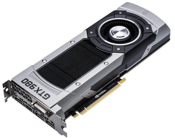
At the risk of sounding like a broken record, the biggest story in the GPU industry over the last year has been over what isn’t as opposed to what is. What isn’t happening is that after nearly 3 years of the leading edge manufacturing node for GPUs at TSMC being their 28nm process, it isn’t being replaced any time soon. As of this fall TSMC has 20nm up and running, but only for SoC-class devices such as Qualcomm Snapdragons and Apple’s A8. Consequently if you’re making something big and powerful like a GPU, all signs point to an unprecedented 4th year of 28nm being the leading node.
We start off with this tidbit because it’s important to understand the manufacturing situation in order to frame everything that follows. In years past TSMC would produce a new node every 2 years, and farther back yet there would even be half-nodes in between those 2 years. This meant that every 1-2 years GPU manufacturers could take advantage of Moore’s Law and pack in more hardware into a chip of the same size, rapidly increasing their performance. Given the embarrassingly parallel nature of graphics rendering, it’s this cadence in manufacturing improvements that has driven so much of the advancement of GPUs for so long.
With 28nm however that 2 year cadence has stalled, and this has driven GPU manufacturers into an interesting and really unprecedented corner. They can’t merely rest on their laurels for the 4 years between 28nm and the next node – their continuing existence means having new products every cycle – so they instead must find new ways to develop new products. They must iterate on their designs and technology so that now more than ever it’s their designs driving progress and not improvements in manufacturing technology.
What this means is that for consumers and technology enthusiasts alike we are venturing into something of an uncharted territory. With no real precedent to draw from we can only guess what AMD and NVIDIA will do to maintain the pace of innovation in the face of manufacturing stagnation. This makes this a frustrating time – who doesn’t miss GPUs doubling in performance every 2 years – but also an interesting one. How will AMD and NVIDIA solve the problem they face and bring newer, better products to the market? We don’t know, and not knowing the answer leaves us open to be surprised.
Out of NVIDIA the answer to that has come in two parts this year. NVIDIA’s Kepler architecture, first introduced in 2012, has just about reached its retirement age. NVIDIA continues to develop new architectures on roughly a 2 year cycle, so new manufacturing process or not they have something ready to go. And that something is Maxwell.
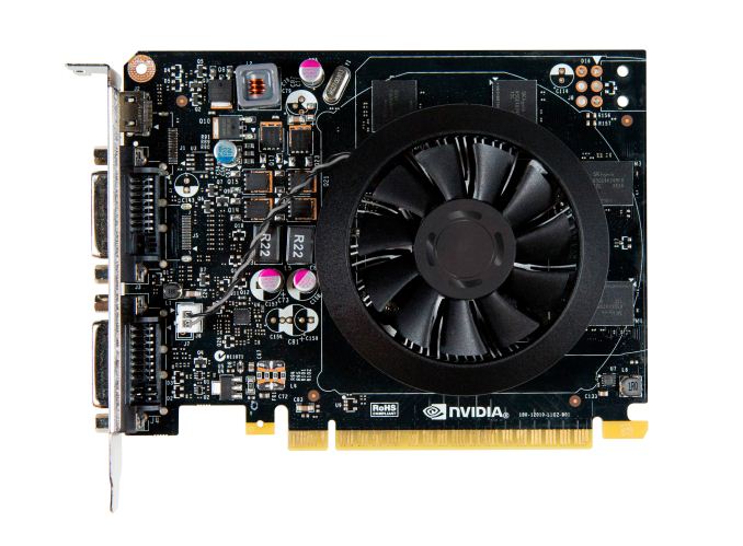
GTX 750 Ti: First Generation Maxwell
At the start of this year we saw the first half of the Maxwell architecture in the form of the GeForce GTX 750 and GTX 750 Ti. Based on the first generation Maxwell GM107 GPU, NVIDIA did something we still can hardly believe and managed to pull off a trifecta of improvements over Kepler. GTX 750 Ti was significantly faster than its predecessor, it was denser than its predecessor (though larger overall), and perhaps most importantly consumed less power than its predecessor. In GM107 NVIDIA was able to significantly improve their performance and reduce their power consumption at the same time, all on the same 28nm manufacturing node we’ve come to know since 2012. For NVIDIA this was a major accomplishment, and to this day competitor AMD doesn’t have a real answer to GM107’s energy efficiency.
However GM107 was only the start of the story. In deviating from their typical strategy of launching high-end GPU first – either a 100/110 or 104 GPU – NVIDIA told us up front that while they were launching in the low end first because that made the most sense for them, they would be following up on GM107 later this year with what at the time was being called “second generation Maxwell”. Now 7 months later and true to their word, NVIDIA is back in the spotlight with the first of the second generation Maxwell GPUs, GM204.
GM204 itself follows up on the GM107 with everything we loved about the first Maxwell GPUs and yet with more. “Second generation” in this case is not just a description of the second wave of Maxwell GPUs, but in fact is a technically accurate description of the Maxwell 2 architecture. As we’ll see in our deep dive into the architecture, Maxwell 2 has learned some new tricks compared to Maxwell 1 that make it an even more potent processor, and further extends the functionality of the family.
| NVIDIA GPU Specification Comparison | ||||||
| GTX 980 | GTX 970 (Corrected) | GTX 780 Ti | GTX 770 | |||
| CUDA Cores | 2048 | 1664 | 2880 | 1536 | ||
| Texture Units | 128 | 104 | 240 | 128 | ||
| ROPs | 64 | 56 | 48 | 32 | ||
| Core Clock | 1126MHz | 1050MHz | 875MHz | 1046MHz | ||
| Boost Clock | 1216MHz | 1178MHz | 928Mhz | 1085MHz | ||
| Memory Clock | 7GHz GDDR5 | 7GHz GDDR5 | 7GHz GDDR5 | 7GHz GDDR5 | ||
| Memory Bus Width | 256-bit | 256-bit | 384-bit | 256-bit | ||
| VRAM | 4GB | 4GB | 3GB | 2GB | ||
| FP64 | 1/32 FP32 | 1/32 FP32 | 1/24 FP32 | 1/24 FP32 | ||
| TDP | 165W | 145W | 250W | 230W | ||
| GPU | GM204 | GM204 | GK110 | GK104 | ||
| Transistor Count | 5.2B | 5.2B | 7.1B | 3.5B | ||
| Manufacturing Process | TSMC 28nm | TSMC 28nm | TSMC 28nm | TSMC 28nm | ||
| Launch Date | 09/18/14 | 09/18/14 | 11/07/13 | 05/30/13 | ||
| Launch Price | $549 | $329 | $699 | $399 | ||
Today’s launch will see GM204 placed into two video cards, the GeForce GTX 980 and GeForce GTX 970. We’ll dive into the specs of each in a bit, but from an NVIDIA product standpoint these two parts are the immediate successors to the GTX 780/780Ti and GTX 770 respectively. As was the case with GTX 780 and GTX 680 before it, these latest parts are designed and positioned to offer a respectable but by no means massive performance gain over the GTX 700 series. NVIDIA’s target for the upgrade market continues to be owners of cards 2-3 years old – so the GTX 600 and GTX 500 series – where the accumulation of performance and feature enhancements over the years adds up to the kind of 70%+ performance improvement most buyers are looking for.
At the very high end the GTX 980 will be unrivaled. It is roughly 10% faster than GTX 780 Ti and consumes almost 1/3rd less power for that performance. This is enough to keep the single-GPU performance crown solidly in NVIDIA’s hands, maintaining a 10-20% lead over AMD’s flagship Radeon R9 290X. Meanwhile GTX 970 should fare similarly as well, however as our sample is having compatibility issues that we haven’t been able to resolve in time, that is a discussion we will need to have another day.
NVIDIA will be placing the MSRP on the GTX 980 at $549 and the GTX 970 at $329. Depending on what you’re using as a baseline, this is either a $50 increase over the last price of the GTX 780 and launch price of the GTX 680, or a roughly $100 price cut compared to the launch prices of the GTX 780 and GTX 780 Ti. Meanwhile GTX 970 is effectively a drop-in replacement for GTX 770, launching at the price that GTX 770 has held for so long. We should see both GPUs at the usual places, though at present neither Newegg nor Amazon is showing any inventory yet – likely thanks to the odd time of launch as this coincides with NVIDIA's Game24 event – but you can check on GTX 980 and GTX 970 tomorrow.
| Fall 2014 GPU Pricing Comparison | |||||
| AMD | Price | NVIDIA | |||
| Radeon R9 295X2 | $1000 | ||||
| $550 | GeForce GTX 980 | ||||
| Radeon R9 290X | $500 | ||||
| Radeon R9 290 | $400 | ||||
| $330 | GeForce GTX 970 | ||||
| Radeon R9 280X | $280 | ||||
| Radeon R9 285 | $250 | ||||
| Radeon R9 280 | $220 | GeForce GTX 760 | |||
Finally, on a housekeeping note today’s article will be part of a series of articles on the GTX 980 series. As NVIDIA has only given us about half a week to look at GTX 980, we are splitting up our coverage to work within the time constraints. Today we will be covering GTX 980 and the Maxwell 2 architecture, including its construction, features, and the resulting GM204 GPU. Next week we will be looking at GTX 980 SLI performance, PCIe bandwidth, and a deeper look at the image quality aspects of NVIDIA’s newest anti-aliasing technologies, Dynamic Super Resolution and Multi-Frame sampled Anti-Aliasing. Finally, we will also be taking a look at the GTX 970 next week once we have a compatible sample. So stay tuned for the rest of our coverage on the Maxwell 2 family.
Maxwell 1 Architecture: The Story So Far
Before we dive into the story and architecture of Maxwell 2, we’d like to spend a bit of time recapping what we’ve seen so far with Maxwell 1 and the GM107 GPU. While both GPUs are distinctly Maxwell, Maxwell 2 is essentially a second, more feature-packed version of Maxwell. Meanwhile it retains all of the base optimizations that went into Maxwell 1, implemented on a larger scale for a larger GPU.
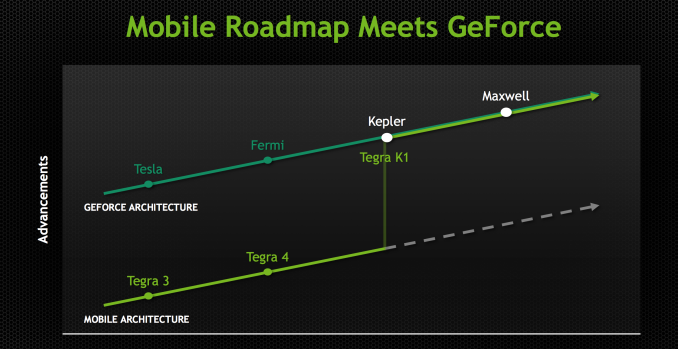
Beginning with the Maxwell family of architectures, NVIDIA embarked on a “mobile first” design strategy for GPUs, marking a significant change in NVIDIA’s product design philosophy. As of Maxwell NVIDIA’s top-down philosophy that saw the launch of high-end desktop class GPUs come first has come to an end, and as NVIDIA has chosen to embrace power efficiency and mobile-friendly designs as the foundation of their GPU architectures, this has led to them going mobile first on Maxwell. With Maxwell NVIDIA has made the complete transition from top to bottom, and are now designing GPUs bottom-up instead of top-down.
By going mobile first NVIDIA is aiming to address several design considerations at all once. First and foremost is the fact that NVIDIA is heavily staking the future of their company in mobile, and that means they need GPU designs suitable for such a market. This mobile first view is primarily focused on SoC-class products – the Tegra family – but really it even extends to mobile PC form factors such as laptops, where discrete GPUs can play an important role but are going to have strict thermal requirements. By designing GPUs around mobile first, NVIDIA starts with a design that is already suitable for Tegra and then can scale it up as necessary for laptop and desktop GeForce products. Graphics is – as we like to say – embarrassingly parallel, so if you can build one small module then it’s relatively easy to scale up performance by building chips with more modules and tying them together. This is the mobile first philosophy.
What this means is that NVIDIA is focused on power efficiency more than ever before. The SoC market is brutal for both the demands placed on the hardware and for the competitive nature of that market, and given the fact that SoCs are so heavily constrained by thermal and power considerations, every bit of power saved can be reinvested in additional performance. This in turn calls for a GPU that is especially power efficient, as it is efficiency that will win the market for NVIDIA.
Maxwell then is an interesting take on NVIDIA’s designs that does not radically alter NVIDIA’s architecture, but has had every accommodation made to improve energy efficiency. The result is a Kepler-like architecture with a number of small design tweaks that improve efficiency in some manner. As NVIDIA tells it, there is no single aspect of Maxwell that is disproportionally responsible for NVIDIA’s energy improvements, but rather it is the culmination of these small changes. Through these changes NVIDIA has been able to come close to doubling their performance per watt versus Kepler, which is nothing short of amazing given the fact that all of this is being done on the same 28nm process as Kepler.
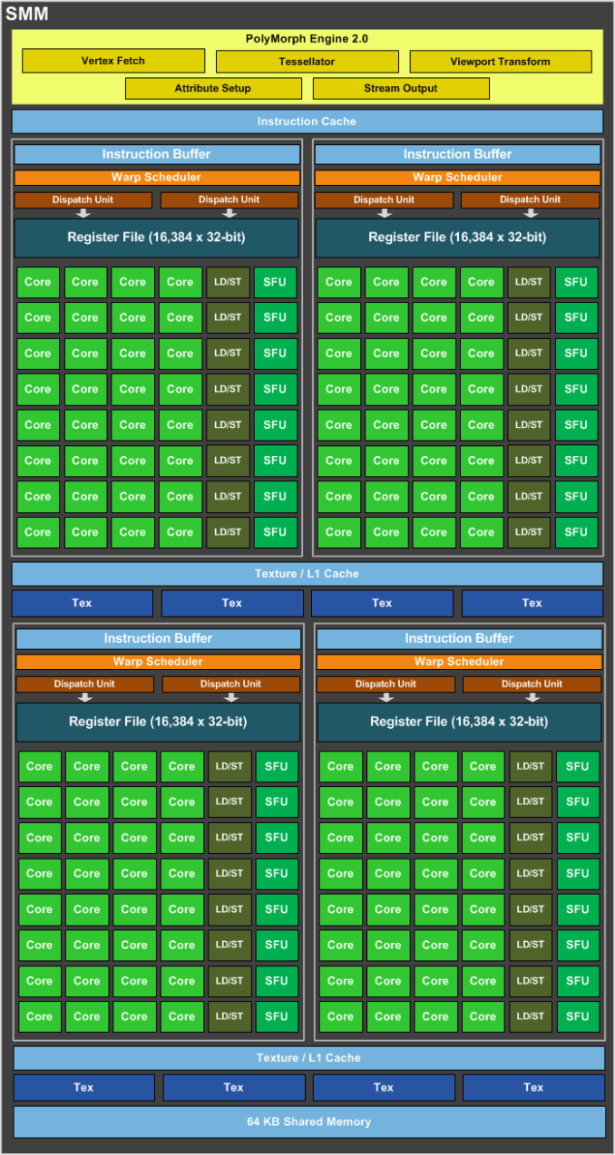
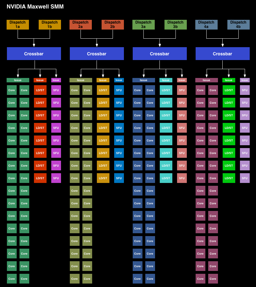
Starting with the Maxwell 1 SMM, NVIDIA has adjusted their streaming multiprocessor layout to achieve better efficiency. Whereas the Kepler SMX was for all practical purposes a large, flat design with 4 warp schedulers and 15 different execution blocks, the SMM has been heavily partitioned. Physically each SMM is still one contiguous unit, not really all that different from an SMX. But logically the execution blocks which each warp scheduler can access have been greatly curtailed.
The end result is that in an SMX the 4 warp schedulers would share most of their execution resources and work out which warp was on which execution resource for any given cycle. But on an SMM, the warp schedulers are removed from each other and given complete dominion over a far smaller collection of execution resources. No longer do warp schedulers have to share FP32 CUDA cores, special function units, or load/store units, as each of those is replicated across each partition. Only texture units and FP64 CUDA cores are shared.
Among the changes NVIDIA made to reduce power consumption, this is among the greatest. Shared resources, though extremely useful when you have the workloads to fill them, do have drawbacks. They’re wasting space and power if not fed, the crossbar to connect all of them is not particularly cheap on a power or area basis, and there is additional scheduling overhead from having to coordinate the actions of those warp schedulers. By forgoing the shared resources NVIDIA loses out on some of the performance benefits from the design, but what they gain in power and space efficiency more than makes up for it.
NVIDIA still isn’t sharing hard numbers on SMM power efficiency, but for space efficiency a single 128 CUDA core SMM can deliver 90% of the performance of a 192 CUDA core SMX at a much smaller size.
Moving on, along with the SMM layout changes NVIDIA has also made a number of small tweaks to improve the IPC of the GPU. The scheduler has been rewritten to avoid stalls and otherwise behave more intelligently. Furthermore by achieving higher utilization of their existing hardware, NVIDIA doesn’t need as many functional units to hit their desired performance targets, which in turn saves on space and ultimately power consumption.
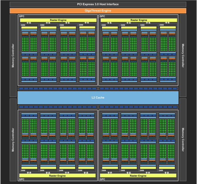
NVIDIA has also been focused on memory efficiency, both for performance and power reasons, resulting in the L2 cache size been greatly increased. NVIDIA has from 256KB in GK107 to 2MB on GM107, and from 512KB on GK104 to the same 2MB on GM204. This cache size increase reduces the amount of traffic that needs to cross the memory bus, reducing both the power spent on the memory bus and improving overall performance.
Increasing the amount of cache always represents an interesting tradeoff since cache is something of a known quantity and is rather dense, but it’s only useful if there are memory stalls or other memory operations that it can cover. Consequently we often see cache implemented in relation to whether there are any other optimizations available. In some cases it makes more sense to use the transistors to build more functional units, and in other cases it makes sense to build the cache. The use of 2MB of L2 cache in both GM107 and GM204 – despite the big differences in ROP count and memory bus size – indicates that NVIDIA’s settling on 2MB as their new sweet spot for consumer graphics GPUs.
Finally there’s the lowest of low level optimizations, which is transistor level optimizations. These optimizations are something of a secret sauce for NVIDIA, but they tell us they’ve gone through at the transistor level to squeeze out additional energy efficiency as they could find it. Given that TSMC 28nm is now a very mature process with well understood abilities and quirks, NVIDIA should be able to design and build their circuits to a tighter tolerance now than they would have been able to when working on GK107 and GK104 over 2 years ago.
Maxwell 2 Architecture: Introducing GM204
Now that we’ve had a chance to recap Maxwell 1 and what went into that architecture, let’s talk about the first of the second generation Maxwell GPUs, the GM204.
GM204 may be a second generation Maxwell part, but it is without question still a Maxwell part. Maxwell has learned some new tricks that we are going to cover here, but functionally speaking you can consider GM204 to be a bigger version of GM107, taking more SMMs and more ROP/memory partitions and using them to build a bigger, more powerful GPU.
With GM107 being built from 5 SMMs, GM204 is a bit more than a triple GM107. Altogether NVIDIA is building GM204 out of 16 SMMs, this time divided up into 4 GPCs instead of GM107’s single GPC. This is bound to 64 ROPs and 4 64bit memory controllers, which is a 4x increase in the number of ROPs compared to GM107, and a 2x increase in the memory bus size.
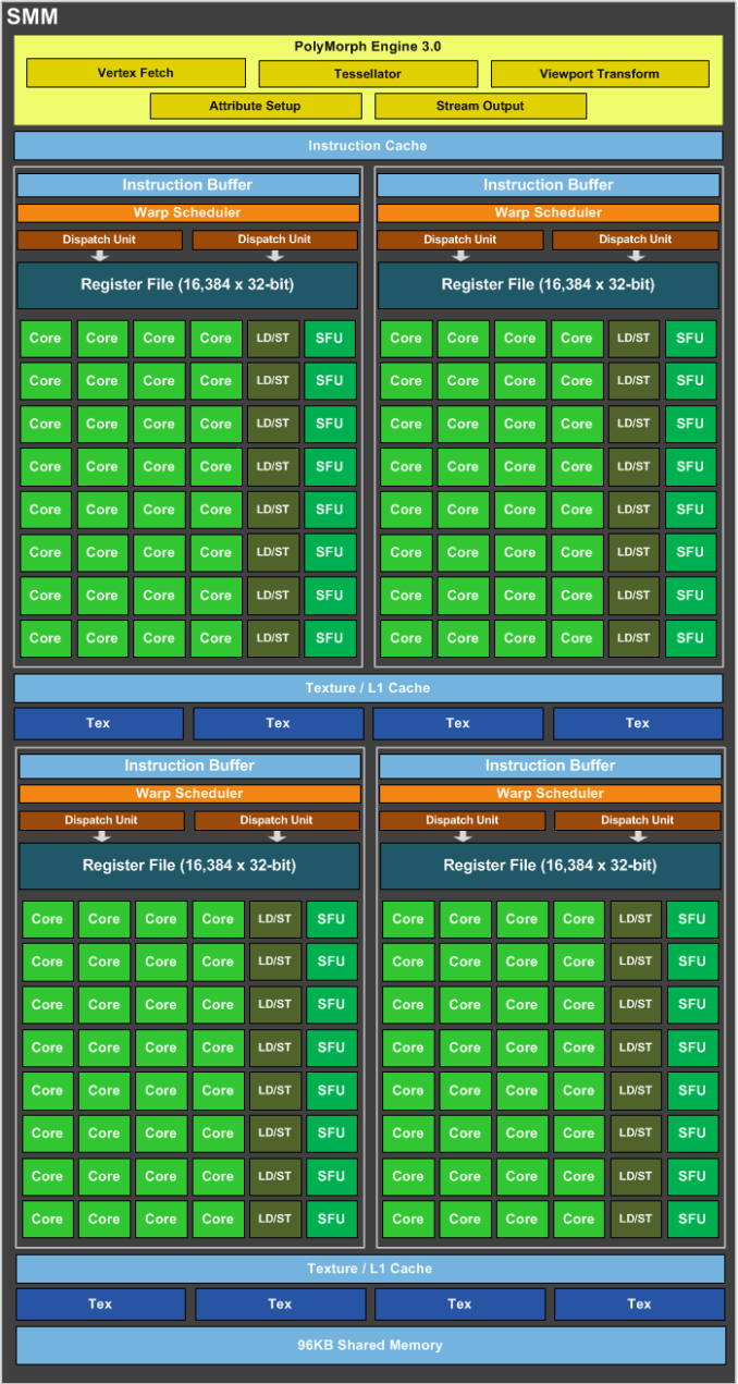
Drilling down to the SMMs for a second, there are a couple of small changes that need to be noted. Organizationally the GM204 SMM is identical to the GM107 SMM, however GM204 gets 96KB of shared memory versus 64KB on GM107. Separate from the combined L1/texture cache, this shared memory services a pair of SMMs and their associated texture units to further reduce the need to go to L2 cache or beyond.
The Polymorph Engines have also been updated. There are not any major performance differences with the 3.0 engines, but they are responsible for implementing some of the new functionality we’ll reference later.
Other than this, GM204’s SMM is identical to the GM107 SMM. This includes the use of 4 shared texture units per 2 SMMs, leading to a 16:1 compute-to-texture ratio, and a 512Kb register file for each SMM.
Compared to GK104 of course this is a more remarkable change. Compared to its immediate predecessor, GM204 sees significant differences in both the layout of the SMM and of the resulting chip, which means that even before accounting for feature differences we can’t just start counting functional units and directly comparing GM204 to GK104. GM204 is overall a more efficient chip, and although it possesses just 33% more CUDA cores than GK104 its performance advantage is much greater, on the order of 50% or more, highlighting the fact that NVIDIA is getting more work out of their CUDA cores than ever before. Altogether, NVIDIA tells us that on average they’re getting 40% more performance per core, which is one of the reasons why GTX 980 can beat even the full GK110 based GTX 780 Ti, with its 2880 CUDA cores.
Compute hardware aside, fleshing out GM204 is of course the ROP/memory partitions. Although the constituent hardware hasn’t changed much – we’re still looking at 7GHz GDDR5 memory controllers and the same pixel throughput per ROP – GM204 is very atypical for its configuration of these parts.
Until now, high-end NVIDIA designs have used an 8:1 ratio; 8 ROPs (or rather ROPs that process 8 pixels per clock) paired up with each 64bit memory controller. This gave GK104 32 ROPs, GK110 48 ROPs, and GM107 16 ROPs. However beginning with GM204 NVIDIA has increased the ROP-to-memory ratio and as a result has doubled their total ROP count compared to GK104. GM204 features a 16:1 ratio, giving us our first NVIDIA GPU with 64 ROPs.
Now the subject of ROPs is always a dicey one because of the nature of pixel operations. Unlike compute hardware, which can be scaled up rather effectively with more complex workloads and better caching methods, the same is not true for ROPs. ROPs are the ultimate memory bandwidth burner. They are paired with memory controllers specifically because the work they do – the Z testing, the pixel blending, the anti-aliasing – devours immense amounts of bandwidth. As a result, even if you are bottlenecked by ROP performance increasing the ROP count won’t necessarily be performance effective if those ROPs are going to be bandwidth starved.
| NVIDIA ROP To Memory Controller Ratios | |||||
| GPU | ROP:MC Ratio | Total ROPs | |||
| Maxwell (GM204) | 16:1 | 64 | |||
| Maxwell (GM107) | 8:1 | 16 | |||
| Kepler (GK110) | 8:1 | 48 | |||
| Fermi (GF110) | 8:1 | 48 | |||
| GT200 | 4:1 | 32 | |||
The last time NVIDIA increased their ROP ratio was for Fermi, when it went from 4:1 to 8:1. This was largely fueled by the introduction of GDDR5, whose higher data rates provided the bandwidth necessary to feed the greater number of ROPs. Since then GDDR5 clockspeeds have increased a bit for NVIDIA, from 4GHz to 7GHz, but so have ROP clockspeeds as well, meaning there hasn’t been a significant change in the ability for NVIDIA’s memory controllers to feed their ROPs since Fermi.
Consequently making the jump to a 16:1 means that change would need to happen somewhere else. This has led to NVIDIA approaching the problem from the other direction: instead of increasing the available memory bandwidth, what can they do to reduce it?
Color Compression
The solution, and really the key to making a 16:1 ROP ratio feasible, is the latest generation of NVIDIA’s delta color compression technology. Color compression in and of itself is not new technology, but over successive hardware generations NVIDIA has continued to iterate on it, and as such has continued to increase the amount of data they can compress.
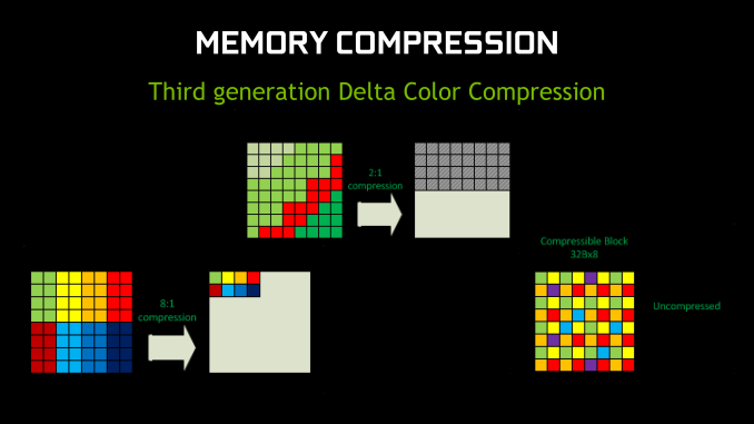
NVIDIA first introduced color compression on the GeForce FX series, where it could compress data at up to a 4:1 ratio. The actual compressibility of any frame would in turn depend on the contents of the frame. At a most basic level NVIDIA would break down a frame into regions and then attempt to find smaller portions of redundant data to compress. Anti-aliasing was especially favorable here, as anti-aliasing samples would frequently all be of a fully covered triangle, resulting in all pixels being identical. In the case of regular color compression the key is finding whole regions of identical colors, at which point you could potentially compress them down by as much as 8:1.
More recently, in Fermi NVIDIA introduced delta color compression, which is designed to take color compression beyond simple regions containing identical pixels. Delta color compression is essentially focused on pattern compression instead of region compression, compressing based on the differences (delta) between pixels rather than how they’re identical; if you can describe how the pixels will differ from one-another, then you can save space describing the delta instead of the individual pixel. Delta color compression works off of the same blocks and essentially applies different delta patterns to them, attempting to find the best pattern for the block.
Delta compression is by its nature less efficient than whole color compression, topping out at just 2:1 compared to 8:1 for the latter. However a 2:1 ratio is still potentially a 50% reduction in data size, which is far better than letting the data go uncompressed. At 4x2 32bit pixels per region, this would mean reducing a region from 32 bytes to 16 bytes.
NVIDIA’s 3rd generation of color compression then is the latest iteration on this technology. The fundamentals between the various generations of delta color compression have not changed, but with each iteration NVIDIA has gained the ability to apply more and more patterns to the blocks to find better matches. 3rd generation delta color compression offers the most patterns yet, and the most opportunity to compress pixel blocks.
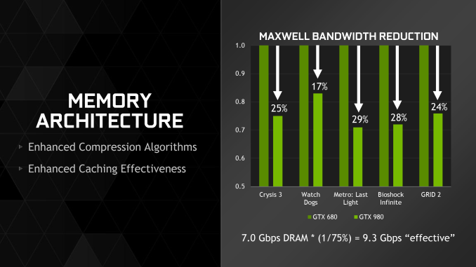
The importance of color compression cannot be understated. The impact of 3rd generation delta color compression is enough to reduce NVIDIA’s bandwidth requirements by 25% over Kepler, and again this comes just from having more delta patterns to choose from. In fact color compression is so important that NVIDIA will actually spend multiple cycles trying different compression ratios, simply because the memory bandwidth is more important than the computational time.
Getting back to our ROPs then, it’s the introduction of 3rd generation color compression, which alongside the larger 2MB L2 cache, makes a 16:1 ROP ratio on GM204 viable. Being able to feed 64 ROPs in turn helps NVIDIA’s overall performance, especially at higher resolutions. With 4K monitors taking off NVIDIA needs to be able to offer competitive performance at those resolutions, and while doubling the number of ROPs won’t double NVIDIA’s performance, it none the less is an essential part of being able to scale up performance for the needs of 4K. AMD for their part already went to 64 ROPs on their high-end GPU with Hawaii last year, and while the subject isn’t nearly as simple as just comparing ROP counts, it was one of the factors that resulted in the superior 4K performance scaling we saw from Hawaii cards.
Die Size & Power
Last but certainly not least, now that we’ve had a chance to discuss the architecture of GM204, let’s talk about its physical properties.
One of the problems posed by remaining on the 28nm process is that increasing CUDA core counts will result in larger GPUs. NVIDIA has actually done quite a bit of work on chip density, and as a result the increase in chip size is not going to be as great as the increase in the underlying hardware. Still, GM204 is a more powerful and more complex chip than GK104, and as a result die size and transistor count has gone up.
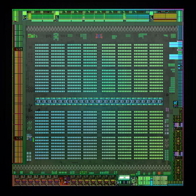
GM204 ends up weighing in at 5.2 billion transistors, with a die size of 398mm2. This compares to 3.54B transistors and a die size of 294mm2 for GK104, and 7.1B transistors and 551mm2 for GK110. Compared to either Kepler design the overall transistor density is improved, albeit not significantly so.
More important is the fact that GM204 ends up being NVIDIA’s largest xx4 class GPU. xx4 GPUs are typically NVIDIA’s midrange to high-end consumer workhorses, designed first and foremost for graphics and not packing the advanced compute features such as high speed FP64 and ECC memory support that we see in the big x00/x10 GPUs. For cost and overlap reasons NVIDIA’s sweet spot up until now has been around 300-350mm2, with GK104 coming in a hair ahead of the curve. But at just shy of 400mm2, GM204 is encroaching on newer, larger territory.
To some degree this is an inevitable result of remaining on the 28nm process. More performance requires more transistors, and as a result die size was destined to go up. None the less the fact that NVIDIA is fabricating such a large GPU as an xx4 GPU is remarkable. It provides a good example of just how much hardware (in terms of transistors) NVIDIA had to throw in to reach their performance goals. Alternatively, it’s telling that NVIDIA is now going to be able to use a 398mm2 chip as the basis of their high-end consumer video card, as opposed to having to use a 551mm2 chip in the form of GK110.
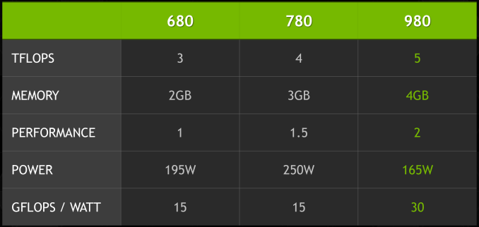
What’s particularly interesting though is that despite the big die, NVIDIA’s power consumption is exceptionally low. By historical standards GK104 was already a low power GPU for its size, this being the case particularly for GTX 680. GTX 680 was a 195W TDP part with a GPU Boost 1.0 power target of 170W. The GM204 based GTX 980 on the other hand, despite packing in nearly 1.5B more transistors for another 104mm2 of die size, actually consumes less power than said GK104 based card. At 165W TDP NVIDIA’s energy efficiency optimizations are in full effect, and it means NVIDIA consumes surprisingly little power for such a large GPU.
Impressively, all of this comes at the same time that NVIDIA is clocking the GPU at over 1.2GHz. This means we are not looking at a simple case of wide-and-slow, as is often the case for power optimized GPUs (see: SoCs). NVIDIA is clocking GM204 high and hitting it with over 1.2v, and yet it’s still able to maintain a 165W TDP in spite of its large die size. We’ll look at the competitive ramifications of this later, but to keep power consumption so low on such a large GPU really is a feather in NVIDIA’s cap.
Maxwell 2’s New Features: Direct3D 11.3 & VXGI
When NVIDIA introduced the Maxwell 1 architecture and the GM107 based GTX 750 series, one of the unexpected aspects of their decision was to release these parts as members of the existing 700 series rather than a newer series to communicate a difference in features. However as it turned out there really wasn’t a feature difference between it and Kepler; other than a newer NVENC block, Maxwell 1 was for all intents and purposes an optimized Kepler architecture. It was the same features built upon the efficiency improvements of the Maxwell architecture.
With that in mind, along with the hardware/architectural changes we’ve listed earlier, the other big factor that sets Maxwell 2 apart from Maxwell 1 is its feature set. In that respect Maxwell 2 is almost a half-generational update on its own, as it implements a number of new features that were not present in Maxwell 1. This means Maxwell 2 is bringing some new features that we need to cover, but it also means that the GM204 based GTX 900 series is feature differentiated from the GTX 600/700 series in a way that the earlier GTX 750 series was not.
Direct3D 11.3
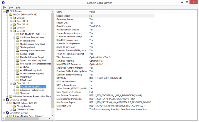
First and foremost among Maxwell 2’s new features is the inclusion of full Direct3D 11.2/11.3 compatibility. Kepler and Maxwell 1 before it were officially feature level 11_0, but they contained an almost complete set of FL 11_1 features, allowing most of these features to be accessed through cap bits. With Maxwell 2 however, NVIDIA has finally implemented the remaining features required for FL11_1 compatibility and beyond, updating their architecture to support the 16x raster coverage sampling required for Target Independent Rasterization and UAVOnlyRenderingForcedSampleCount.
This extended feature set also extends to Direct3D 11.2, which although it doesn’t have an official feature level of its own, does introduce some new (and otherwise optional) features that are accessed via cap bits. Key among these, Maxwell 2 will support the more advanced Tier 2 tiled resources, otherwise known as sparse textures or partially resident textures. Tier 2 was introduced into the specification to differentiate the more capable AMD implementation of this feature from NVIDIA’s hardware, and now as of Maxwell 2 NVIDIA can support the more advanced functionality required for Tier 2.
Finally, Maxwell will also support the features being introduced in Direct3D 11.3 (and made available to D3D 12), which was announced alongside Maxwell at NVIDIA’s editors’ day event. We have a separate article covering Direct3D 11.3, so we won’t completely retread that ground here, but we will cover the highlights.
The forthcoming Direct3D 11.3 features, which will form the basis (but not entirety) of what’s expected to be feature level 11_3, are Rasterizer Ordered Views, Typed UAV Load, Volume Tiled Resources, and Conservative Rasterization. Maxwell 2 will offer full support for these forthcoming features, and of these features the inclusion of volume tiled resources and conservative rasterization is seen as being especially important by NVIDIA, particularly since NVIDIA is building further technologies off of them.
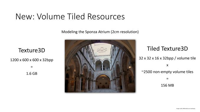
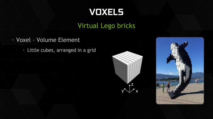
Volume tiled resources is for all intents and purposes tiled resources extended into the 3rd dimension. Volume tiled resources are primarily meant to be used with 3D/volumetric pixels (voxels), with the idea being that with sparse allocation, volume tiles that do not contain any useful information can avoid being allocated, avoiding tying up memory in tiles that will never be used or accessed. This kind of sparse allocation is necessary to make certain kinds of voxel techniques viable.
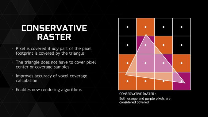
Meanwhile conservative rasterization is also new to Maxwell 2. Conservative rasterization is essentially a more accurate but performance intensive solution to figuring out whether a polygon covers part of a pixel. Instead of doing a quick and simple test to see if the center of the pixel is bounded by the lines of the polygon, conservative rasterization checks whether the pixel covers the polygon by testing it against the corners of the pixel. This means that conservative rasterization will catch cases where a polygon was too small to cover the center of a pixel, which results in a more accurate outcome, be it better identifying pixels a polygon resides in, or finding polygons too small to cover the center of any pixel at all.
Conservative rasterization is being added to Direct3D in order to allow new algorithms to be used which would fail under the imprecise nature of point sampling. Like VTR, voxels play a big part here as conservative rasterization can be used to build a voxel. However it also has use cases in more accurate tiling and even collision detection. This feature is technically possible in existing hardware, but the performance of such an implementation would be very low as it’s essentially a workaround for the lack of necessary support in the rasterizers. By implementing conservative rasterization directly in hardware, Maxwell 2 will be able to perform the task far more quickly, which is necessary to make the resulting algorithms built on top of this functionality fast enough to be usable.
VXGI
Outside of the features covered by Direct3D 11.3, NVIDIA will also be adding features specifically to drive a new technology they are calling Voxel accelerated Global Illumination (VXGI).
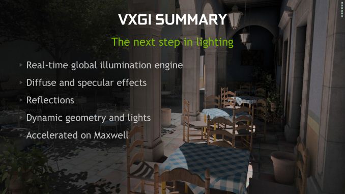
At the highest level, VXGI is a manner of implementing global illumination by utilizing voxels in the calculations. Global illumination is something of a holy grail for computer graphics, as it can produce highly realistic and accurate lighting dynamically in real time. However global illumination is also very expensive, the path tracing involved taking up considerable time and resources. For this reason developers have played around with global illumination in the past – the original version of Epic’s Unreal 4 Engine Elemental demo implanted a voxel based global illumination method, for example – but it has always been too slow for practical use.
With VXGI NVIDIA is looking to solve the voxel global illumination problem through a combination of software and hardware. VXGI proper is the software component, and describes the algorithm being used. NVIDIA has been doing considerable research into voxel based global illumination over the years, and has finally reached a point where they have an algorithm ready to go in the form of VXGI.
VXGI will eventually be made available for Unreal Engine 4 and other major game engines starting in Q4 of this year. And while the VXGI greatly benefits from the hardware features built into Maxwell 2, it is not strictly reliant on the hardware and can be implemented through more traditional means on existing hardware. VXGI is if nothing else scalable, with the algorithm being designed to scale up and down with hardware by adjusting the density of the voxel grid, which in turn influences the number of calculations required and the resulting accuracy. Maxwell 2 for its part will be capable of using denser grids due to its hardware acceleration capabilities, allowing for better performance and more accurate lighting.
It’s at this point we’ll take a break and apologize to NVIDIA’s engineers for blowing through VXGI so quickly. This is actually a really interesting technology, as global illumination offers the possibility of finally attaining realistic real-time lighting in any kind of rendered environment. However VXGI is also a complex technology that is a subject in and of itself, and we could spend all day just covering it (we’d need to cover rasterization and path tracing to fully explain it). Instead we’d suggest reading NVIDIA’s own article on the technology once that is posted, as NVIDIA is ready and willing to go into great detail in how the technology works.
Getting back to today’s launch then, the other aspect of VXGI is the hardware features that NVIDIA has implemented to accelerate the technology. Though a big part of VXGI remains brute forcing through the path and cone tracing, the other major aspect of VXGI is building the voxel grids used in these calculations. It’s here where NVIDIA has pulled together the D3D 11.3 feature set, along with additional hardware features, to greatly accelerate the process of creating the voxel grid in order to speed up the overall algorithm.
From the D3D 11.3 feature set, conservative rasterization and volumetric tiled resources will play a big part. Conservative rasterization allows the creation of more accurate voxels, owing to the more accurate determination of whether a pixel/voxel covers a given polygon. Meanwhile volumetric tiled resources will allow for the space efficient storage of voxels, allowing software to store only the voxels it needs and not the many empty voxels that would otherwise be present in a scene.
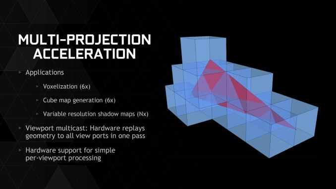
Joining these features as the final VXGI-centric feature for Maxwell 2 is a feature NVIDIA is calling Multi-Projection Acceleration. The idea behind MPA is that there are certain scenarios where the same geometry needs to be projected multiple times – voxels being a big case of this due to being 6 sided – and that for performance reasons it is desirable to do all of these projections much more quickly than simply iterating though every necessary projection in shaders. In these scenarios being able to quickly project geometry to all the necessary surfaces is a significant performance advantage.
A big part of MPA is a sub-feature called viewport multicast. In viewport multicast Maxwell 2 can replay the necessary geometry to all of the viewports in a single pass. At the hardware level this involves giving the hardware the ability to automatically determine when it needs to engage in viewport multicast, based on its understanding of the workload it's receiving. This is once again a case where something is being done in a fixed-function like fashion for performance reasons, rather than being shuffled off to slower shader hardware.
Alongside voxelization, NVIDIA tells us that MPA should also be applicable to cube map generation and shadow map generation. Both of which make plenty of sense in this case: in both scenarios you are projecting the same geometry multiple times, whether it’s to faces of a cube or to shadow maps of increasing resolution. As a result MPA should have some benefits even in renderers that aren’t using VXGI, though clearly the greatest benefits are still going to be when VXGI is in play.
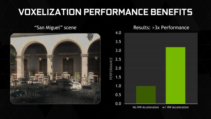
NVIDIA believes that the overall performance improvement to voxelization from these technologies will be very significant. In their own testing of the technology in rendering a scene set in San Miguel de Allende, Mexico (a common test scene for global illumination), NVIDIA has found that Maxwell 2’s hardware acceleration features tripled their voxelization performance.
Overall NVIDIA is heavily betting on VXGI at this time both to further set apart Maxwell 2 based cards from the competition, and to further advance the state of PC graphics. In the gaming space in particular NVIDIA has a significant interest in making sure PC games aren’t just straight console ports that run at higher framerates and resolutions. This is the situation that has spurred on the development of GameWorks and technologies like VXGI, so that game developers can enhance the PC ports of their games with technologies that improve their overall rendering quality. Maxwell 2 in turn is the realization that while some of these features can be performed in software/shaders on today’s hardware, these features will be even more useful and impressive when backed with dedicated hardware to improve their performance.
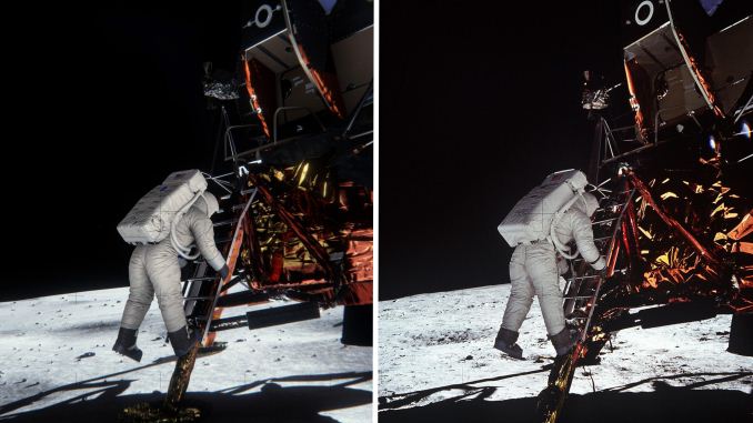
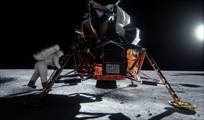
Finally, we’ll close out our look at VXGI with a preview of NVIDIA’s GTX 900 series tech demo, which is a rendered recreation of a photo/scene involving Buzz Aldrin and the Apollo 11 moon landing. The Apollo 11 demo is designed to show off the full capabilities of VXGI, utilizing the lighting technique to correctly and dynamically emulate specular, diffuse, and other forms of lighting that occur in reality. At editors’ day NVIDIA originally attempted to pass off the rendering as the original photo, and while after a moment it’s clear that it’s a rendering – among other things it lacks the graininess of a 1969 film based camera – it comes very, very close. In showcasing the Apollo 11 tech demo, NVIDIA’s hope is that one day games will be able to achieve similarly accurate lighting effects through the use of VXGI.
Display Matters: HDMI 2.0, HEVC, & VR Direct
Stepping away from the graphics heart of Maxwell 2 for a bit, NVIDIA has been busy not just optimizing their architecture and adding graphical features to their hardware, but they have also added some new display-oriented features to the Maxwell 2 architecture. This has resulted in an upgrade of their video encode capabilities, their display I/O capabilities, and even their ability to drive virtual reality headsets such as the Oculus Rift.
We’ll start first with display I/O. HDMI users will be happy to see that as of GM204, NVIDIA now supports HDMI 2.0, which will allow NVIDIA to drive future 4K@60Hz displays over HDMI and without compromise. HDMI 2.0 for its part is the 4K-focused upgrade of the HDMI standard, and brings with it support for the much higher data rate (through a greatly increased clockspeed of 600MHz) necessary to drive 4K displays at 60Hz, while also introducing features such as new subsampling patterns like YCbCr 4:2:0, and official support for wide aspect ratio (21:9 displays).
It should be noted that this is full HDMI 2.0 support, and as a result it notably differs from the earlier support that NVIDIA patched into Kepler and Maxwell 1 through drivers. Whereas NVIDIA’s earlier update was to allow these products to drive a 4K@60Hz display using 4:2:0 subsampling to stay within the bandwidth limitations of HDMI 1.4, Maxwell 2 implements the bandwidth improvements necessary to support 4K@60Hz with full resolution 4:4:4 and RGB color spaces.
Given the timeline for HDMI 2.0 development, the fact that we’re seeing HDMI 2.0 support now is if anything a pleasant surprise, since it’s earlier than we expected it. However this will leave HTPC users in a pickle if they want HDMI 2.0 support; with the GM107 based GTX 750 series having launched only 7 months ago without HDMI 2.0 support, we would not expect NVIDIA’s HTPC-centric video cards to be replaced any time soon. This means the only option for HTPC users wanting HDMI 2.0 support right away is to upgrade to a larger and more powerful Maxwell 2 based card, or otherwise stick to the low powered GTX 750 series and go without HDMI 2.0.
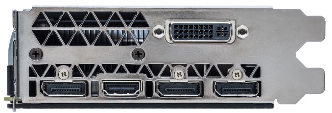
Meanwhile alongside the upgrade to HDMI 2.0, NVIDIA has also made one other change to their display controllers that should be of interest to multi-monitor users. With Maxwell 2, a single display controller can now drive multiple identical MST substreams on its own, rather than requiring a different display controller for each stream. This feature will be especially useful for driving tiled monitors such as many of today’s 4K monitors, which are internally a pair of identical displays driven using MST. By being able to drive both tiles off of a single display controller, NVIDIA can make better use of their 4 display controllers, allowing them to drive up to 4 such displays off of a Maxwell 2 GPU as opposed to the 2 display limitation that is inherent to Kepler GPUs. For the consumer cards we’re seeing today, the most common display I/O configuration will include 3 DisplayPorts, allowing these specific cards to drive up to 3 such 4K monitors.
HEVC & 4K Encoding
In Maxwell 1, NVIDIA introduced updated versions of both their video encode and decode engines. On the decode side the new VP6 decoder increased the performance of the decode block to allow NVIDIA to decode H.264 up to 4K@60Hz (Level 5.2), something the older VP5 decoder was not fast enough to do. Meanwhile the Maxwell 1 NVEC video encoder received a similar speed boost, roughly doubling its performance compared to Kepler.
Surprisingly, even after only 7 months since the first Maxwell 1 GPUs, NVIDIA has once again overhauled NVENC, and this time more significantly. The Maxwell 2 version of NVENC further builds off of the Maxwell 1 NVENC by adding full support for HEVC (H.265) encoding. Like HDMI 2.0 support, this marks the very first PC GPU we’ve seen integrate support for this more advanced codec.
At this point there’s really not much that can be done with Maxwell 2’s HEVC encoder – it’s not exposed in anything or used in NVIDIA’s current tools – but NVIDIA is laying the groundwork for the future once HEVC support becomes more commonplace in other hardware and software. NVIDIA envisions their killer app for HEVC support to be game streaming, where the higher efficiency of HEVC will improve the image quality of game streams due to the limited bandwidth available in most streaming scenarios. In the long run we would expect NVIDIA to utilize HEVC for GameStream for the home, and at the server level support for HEVC in the next generation of GRID cards will be a major boon to NVIDIA’s GRID streaming efforts.
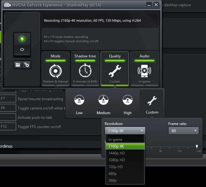
Meanwhile where the enhanced version of NVENC is going to be applicable today is in ShadowPlay. While still recording in H.264, the higher performance of NVENC means that NVIDIA can now offer recording at higher resolutions and bitrates. With GM204 NVIDIA’s hardware can now record at 1440p60 and 4Kp60 at bitrates up to 130Mbps, as opposed to the 1080p60 @ 50Mbps limit for their Kepler cards.
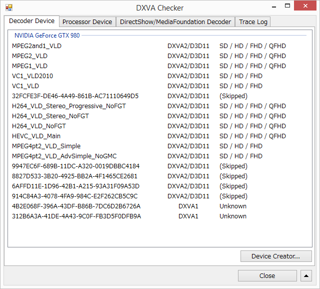
Finally, and somewhat paradoxically, Maxwell 2 inherits Kepler and Maxwell 1’s hybrid HEVC decode support. First introduced with Maxwell 1 and backported to Kepler, NVIDIA’s hybrid HEVC decode support enables HEVC decoding on these parts by using a combination of software (shader) and hardware decoding, leveraging the reusable portions of the H.264 decode block to offload to fixed function hardware what elements it can, and processing the rest in software.
A hybrid decode process is not going to be as power efficient as a full fixed function decoder, but handled in the GPU it will be much faster and more power efficient than handling the process in software. The fact that Maxwell 2 gets a hardware HEVC encoder but a hybrid HEVC decoder is in turn a result of the realities of hardware development for NVIDIA; you can’t hybridize encoding, and the hybrid decode process is good enough for now. So NVIDIA spent their efforts on getting hardware HEVC encoding going first, and at this point we’d expect to see full hardware HEVC decoding show up in a future generation of hardware (and we’d note that NVIDIA can swap VP blocks at will, so it doesn’t necessarily have to be Pascal).
VR Direct
Our final item on the list of NVIDIA’s new display features is a family of technologies NVIDIA is calling VR Direct.
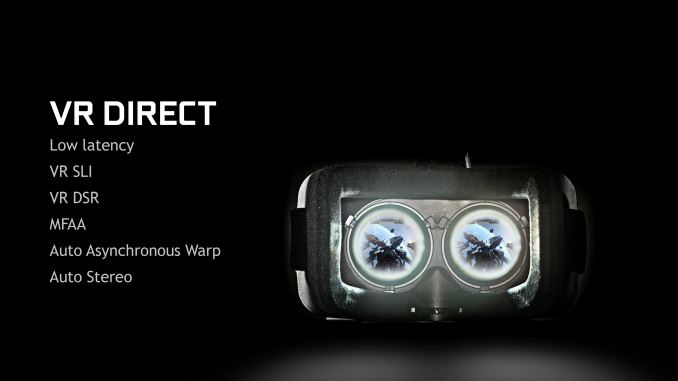
VR Direct in a nutshell is a collection of technologies and software enhancements designed to improve the experience and performance of virtual reality headsets such as the Oculus Rift. From a practical perspective NVIDIA already has some experience in stereoscopic rendering through 3D Vision, and from a marketing perspective the high resource requirements of VR would be good for encouraging GeForce sales, so NVIDIA will be heavily investing into the development of VR technologies through VR Direct.
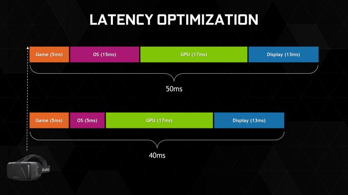
From a technical perspective the biggest thing that Oculus and other VR headset makers need from GPU manufacturers and the other companies involved in the PC ecosystem is methods of reducing the latency/input lag between a user’s input and when a finished frame becomes visible on a headset. While some latency is inevitable – it takes time to gather data and render a frame – the greater the latency the greater the disconnect will be between the user and the rendered world. In more extreme cases this can make the simulation unusable, or even trigger motion sickness in individuals whose minds can’t handle the disorientation from the latency. As a result several of NVIDIA’s features are focused on reducing latency in some manner.
First and foremost, for VR headsets NVIDIA has implemented a low latency mode that minimizes the amount of time a frame spends being prepared by the drivers and OS. In an average case this low latency mode eliminates 10ms of OS-induced latency from the rendering pipeline, and this is the purest optimization of the bunch.
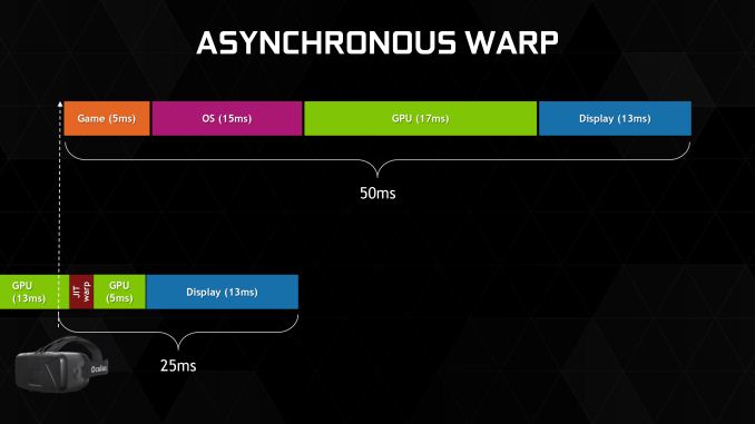
Meanwhile at the more extreme end of the feature spectrum, NVIDIA will be supporting a feature called asynchronous warp. This feature, known by Oculus developers as time warp, involves rendering a frame and then at the last possible moment updating the head tracking information from the user. After that information is acquired, the nearly finished frame then has a post-process warping applied to it to take into account head movement since the frame was initially submitted, with the ultimate goal of this warping being the simulation of what the frame should look like had it been rendered instantaneously.
From a quality perspective asynchronous warp stands to be a bit of a kludge, but it is the single most potent latency improvement among the VR Direct feature set. By modifying the frame to account for the user’s head position as late as is possible, it reduces the perceived latency by as much as 25ms.
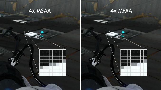
NVIDIA’s third latency optimization is less a VR optimization and more a practical effect of an existing technology, and that is Multi-Frame sampled Anti-Aliasing. As we'll discuss later in our look at this new AA mode, Multi-Frame sampled Anti-Aliasing is designed to offer 4x MSAA-like quality with 2x MSAA-like performance. Assuming a baseline of 4x MSAA, switching it out for Multi-Frame sampled Anti-Aliasing can shave an additional few milliseconds off of the frame rendering time.
Lastly, NVIDIA’s fourth and final latency optimization for VR Direct is VR SLI. And this feature is simple enough: rather than using alternate frame rendering (AFR) to render both eyes at once on one GPU, split up the workload such that each GPU is working on each eye simultaneously. AFR, though highly compatible with traditional monoscopic rendering, introduces additional latency that would be undesirable for VR. By rendering each eye separately on each GPU, NVIDIA is able to apply the performance benefits of SLI to VR without creating additional latency. Given the very high performance and low latencies required for VR, it’s currently expected that most high-end games supporting VR headsets will need SLI to achieve their necessary performance, so being able to use SLI without a latency penalty will be an important part of making VR gaming commercially viable.
On a side note, for the sake of clarity we do want to point out that many of NVIDIA’s latency optimizations come from the best practices suggestions of Oculus VR. Asynchronous warp and OS level latency optimizations for example are features that Oculus VR is suggesting for hardware developers and/or pursuing themselves. So while these features are very useful to have on GeForce hardware, they are not necessarily all ideas that NVIDIA has come up with or technologies that are limited to NVIDIA hardware (or even the Maxwell 2 architecture).
Moving on, other than NVIDIA’s latency reduction technologies the VR Direct feature set will also include some feature improvements designed to improve the quality and usability of VR. NVIDIA’s Dynamic Super Resolution (DSR) technology will be available to VR, and given the physical limits on pixel density in today’s OLED panels it will be an important tool in reducing perceptible aliasing. NVIDIA will also be extending VR support to GeForce Experience at a future time, simplifying the configuration of VR-enabled games. For VR on GeForce Experience NVIDIA wants to go beyond just graphical settings and also auto-configure inputs as well, handling remapping of inputs to head/body tracking for the user automatically.
Ultimately at this point VR Direct is more of a forward looking technology than it is something applicable today – the first consumer Oculus Rift hasn’t even been announced, let alone shipped – but by focusing on VR early NVIDIA is hoping to improve the speed and ease of VR development, and have the underpinnings in place once consumer VR gear becomes readily available.
Better AA: Dynamic Super Resolution & Multi-Frame Sampled Anti-Aliasing
On a personal note, the subject of anti-aliasing has always been near and dear to my heart. When you review video cards for a living you start to see every minor defect, and this is especially the case for jaggies and other forms of aliasing. So when new anti-aliasing modes are being introduced it is always a time of great interest.
Dynamic Super Resolution
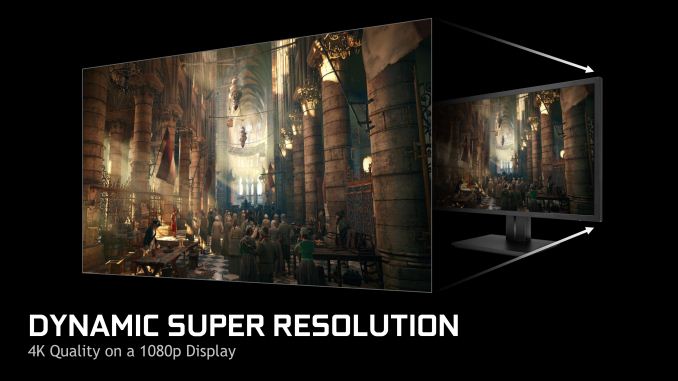
With the launch of Maxwell 2 NVIDIA is going to be launching 2 new anti-aliasing technologies. The first of these technologies is called Dynamic Super Resolution, and it is a sort of brute force anti-aliasing method targeted at games that do not support real anti-aliasing or do not support it well.
In the case of Dynamic Super Resolution (DSR), NVIDIA achieves anti-aliasing by rendering a frame at a resolution higher than the user’s monitor (the Super Resolution of DSR), and then scaling the image back down to the monitor’s native resolution. This process of rendering at a higher resolution and then blending pixels together when the image is scaled down results in a higher quality image that is less aliased than an image rendered at a native resolution, owing to the additional detail attained from rendering at a higher resolution.
Although NVIDIA is first introducing DSR with Maxwell 2 GPUs, the technique is actually much older than that. For enthusiasts this process is better known as downsampling, and while it has been around for years it has been relatively inaccessible to the masses due to the hacky nature of unsupported downsampling, which among other things requires tweaking settings for monitors, drivers, and games all alike. As a result while NVIDIA can’t lay claim to the idea of downsampling, this is still a significant improvement in the downsampling process because downsampling is now being promoted to a first-class feature, which means it brings with it the full development backing of NVIDIA and the wider accessibility that will bring.
Of course it should also be noted that NVIDIA and enthusiasts aren’t the only parties who have been engaging in downsampling, as game developers as well have periodically been adding the feature directly to their games. Among our benchmarking suite, Battlefield 4, Company of Heroes 2, and Thief all support the equivalent of downsampling; BF4 and CoH2 allow a game to be internally rendered at a higher resolution, and Thief has SSAA modes that do the same thing. As a result there are already some games on the market that utilize downsampling/DSR, with the difference/advantage of NVIDIA’s implementation being that it makes the technique accessible to games that do not implement it on their own.
Digging a bit deeper, the image quality advantage of downsampling/DSR is that it’s fundamentally a form of Super Sample Anti-Aliasing (SSAA). By rendering an image at a higher resolution and then scaling it down, DSR is essentially sampling each pixel multiple times, improving the resulting image quality by removing geometry, texture, and shader aliasing. And like true SSAA, DSR is going to be very expensive from a rendering standpoint – you’re potentially increasing your frame resolution by 4x – but if you have the performance to spare then DSR will be worth it, and this is the basis of NVIDIA’s inclusion of DSR as a first-class feature.
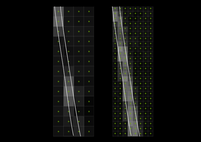
Meanwhile from an image quality standpoint DSR should be a decent but not spectacular form of SSAA. Because it’s simply rendering an image at a larger size, DSR functionally uses an ordered pixel grid. For anti-aliasing purposes ordered grids are suboptimal due to the fact that near-vertical and near-horizontal geometry doesn’t get covered well, which is why true AA techniques will use rotated grids or sparse grids. None the less while DSR’s resulting sample pattern isn’t perfect it is going to be much better than the alternative of forgoing anti-aliasing entirely.

Anti-Aliasing Example: Ordered Grid vs. Rotated Grid (Images Courtesy Beyond3D)
DSR to that end can be considered a sort of last-resort method of SSAA. For games that support proper RG/SG SSAA, those anti-aliasing methods will produce superior results. However as a number of games do not support native anti-aliasing of any kind due to the use of deferred renderers, DSR provides a way to anti-alias these games that is compatible with their rendering methods.
Moving on, under the hood NVIDIA is implementing DSR as a form of high resolution rendering combined with a 13-tap Gaussian filter. In this process NVIDIA’s drivers present a game with a fake resolution higher than the actual monitor (i.e. 3840x2160 for a true 1080p monitor), and then have the game render to that higher resolution while using the Gaussian filter to blend the results down to the lower resolution. The fact that NVIDIA is using a Gaussian filter here as opposed to a simple box filter definitely raises a few eyebrows due to the potential for unwanted blurring, and this is something we will be taking a look at next week in our image quality analysis of GTX 980.
In the meantime the use of downsampling in this fashion means that DSR will have a high but less-than-perfect compatibility rate. Games that can’t render at very high resolutions will not be usable with DSR, and games that render incorrectly at those resolutions will similarly be problematic. In practice many games should be able to render at 4K-like resolutions, but some fraction of those games will not know how to scale up the UI accordingly, resulting in a final UI that is too small after the image is scaled down.
Looking at the broader picture, from a marketing and product perspective DSR is another tool for NVIDIA for dealing with console ports. Games that are ported from current-gen and last-gen consoles and don’t make significant (if any) use of newer GPU features will as a rule of thumb look little-if-any better on the PC than they do their original console. This in turn leaves more powerful GPUs underutilized and provides little incentive to purchase a PC (and an NVIDIA GPU) over said consoles. But by implementing DSR, NVIDIA and NVIDIA users can attain a leg-up on consoles by improving image quality through SSAA. And while this can’t make up for a lack of texture or model quality, it can convincingly deal with the jaggies that would otherwise be present on both the PC and the console.
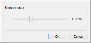
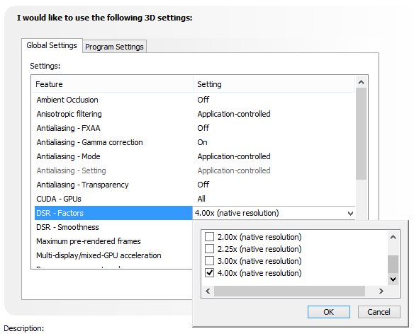
With that in mind, it should be noted that DSR is primarily geared towards low DPI monitor users; 1080p, 900p, 1200p, etc. High DPI monitor users can simply run a game natively at 4K, at which point they likely won’t have much performance left over for any further anti-aliasing anyhow. Meanwhile DSR for its part will support resolution factors of between 1.2x (1.1 x 1.1) and 4x (2 x 2), allowing the resolution used to vary depending on the desired quality level and resulting performance. From a quality perspective 4x will in turn be the best factor to use, as this is the only factor that allows for potentially clean integer scaling (think Retina display). For this reason DSR also offers a smoothness control, which allows the user to control the intensity of the Gaussian filter used.
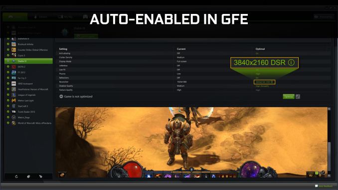
Meanwhile for end users NVIDIA will be exposing DSR at two points. DSR is currently implemented in the NVIDIA control panel, which allows for direct control of the scaling factor and the smoothness on a per-game basis. Meanwhile DSR will also be exposed in GeForce Experience, which can enable DSR for games that NVIDIA has vetted to work with the technology and are running on computers fast enough to render at these higher resolutions.
Finally, while DSR is currently limited to Maxwell 2 video cards, NVIDIA has not-so-subtly been hinting that DSR will in time be ported to NVIDIA’s previous generation cards. The technique itself does not require any special Maxwell 2 hardware and should easily work on Kepler hardware as under the hood it’s really just a driver trick. However whether Kepler cards are fast enough to use DSR with an adequate resolution factor will be another matter entirely.
Multi-Frame Sampled Anti-Aliasing
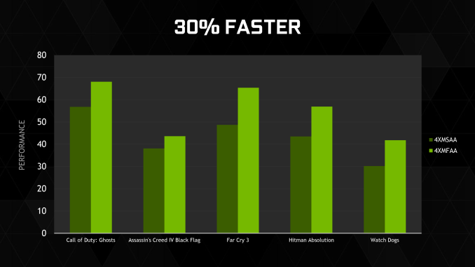
NVIDIA’s other new anti-aliasing technology for Maxwell 2 is the unfortunately named Multi-Frame sampled Anti-Aliasing. Whereas DSR was targeted at the quality segment of the market as a sort of last resort AA method for improving image quality, Multi-Frame Sampled Anti-Aliasing is targeted at the opposite end of the spectrum and is designed to be a more efficient form of MSAA that achieves similar results with half as many samples and half of the overhead.
Unlike DSR, Multi-Frame Sampled Anti-Aliasing is implemented on and requires new Maxwell 2 hardware, which is NVIDIA’s new programmable MSAA sampling pattern ability in their ROPs. This feature allows NVIIDA to dynamically alter their MSAA sample patterns, which is a key feature of Multi-Frame Sampled Anti-Aliasing, and therefore cannot easily be backported to existing hardware.
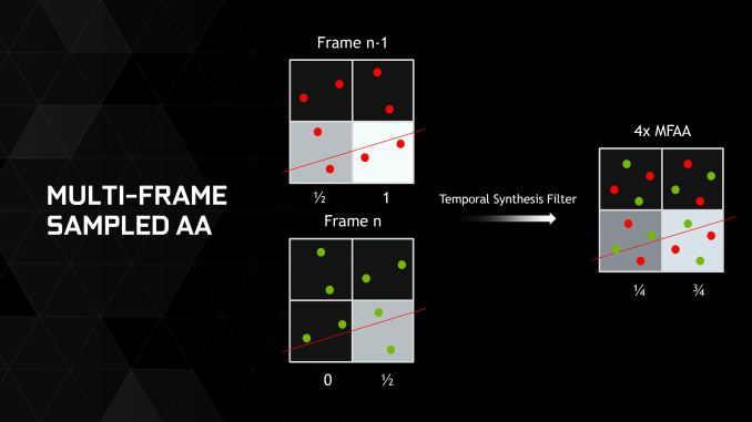
In any case, Multi-Frame Sampled Anti-Aliasing is based on the concept of changing the MSAA sample pattern in every frame, in practice using a 2x (2 sample) MSAA pattern and combining the results from multiple frames to mimic a 4x (4 sample) MSAA pattern. If it’s done right then you should receive results comparable to 4x MSAA with the cost of 2x MSAA.
Once you can grasp the concept of changing sample patterns, the idea is actually relatively simple. And in fact like DSR it has been done before in a lesser form by none other than AMD (or at the time, ATI). In 2004 with their X800 series of cards, AMD launched their Temporal Anti-Aliasing technology, which was based on the same sampling concept but importantly without any kind of frame combining/blending. Over the years Temporal AA never did see much use, and was ultimately discontinued by AMD.
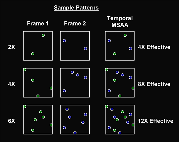
Compare & Contrast: AMD's Discontinued Temporal AA
What sets Multi-Frame Sampled Anti-Aliasing apart from Temporal AA and similar efforts – and why NVIDIA thinks they will succeed where AMD failed – is the concept of temporal reprojection, or as NVIDIA calls it their temporal synthesis filter. By reusing pixels from a previous frame (to use them as pseudo-MSAA samples), the resulting frame can more closely match true 4x MSAA thanks to the presence of multiple samples. The trick is that you can’t simply reuse the entire last frame, as this would result in a much less jagged image that also suffered from incredible motion blur. For this reason the proper/best form of temporal reprojection requires figuring out which specific pixels to reproject and which to discard.
From an image quality standpoint, in the ideal case of a static image this would correctly result in image quality rivaling 4x MSAA. As a lack of camera motion means that the pixels being sampled never changed, the samples would line up perfectly and would fully emulate 4x MSAA. However once in motion the overall image quality is going to be heavily reliant on the quality of the temporal reprojection. In the best case scenario for motion Multi-Frame Sampled Anti-Aliasing still will not perfectly match 4x MSAA, and in the worst case scenario for motion it could still result in either 2x MSAA-like anti-aliasing, significant blurring, or even both outcomes.
Multi-Frame sampled Anti-Aliasing also has one other catch that has to be accounted for, and that’s frame rates. At low framerates – below 30fps – the time between frames grows so large that temporal reprojection would become increasingly inaccurate and the human eyes would pick up on the sample pattern changes, which means that this anti-aliasing technique is only usable with high frame rates. Importantly this is actually one of the benefits of Multi-Frame sampled Anti-Aliasing, as the lower overhead of a 2x sample pattern makes it easier to maintain higher framerates.
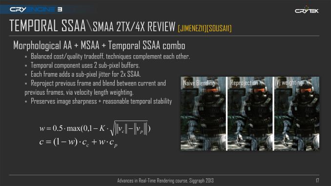
For what it’s worth, while NVIDIA is the first GPU vendor to implement temporal AA with temporal reprojection in their drivers, they are not the first individual overall. Over the years a few different game engines have implemented AA with temporal reprojection, the most notable of which is Crytek’s CryEngine 3. In Crysis 3 temporal reprojection was implemented as part of the SMAA anti-aliasing technique. The result was effective at times, but SMAA does result in some blurring, though this is difficult to separate from the effects of morphological filtering in SMAA. In any case the point is that while we will reserve our final comments for our evaluation of Multi-Frame sampled Anti-Aliasing, we are expecting that it will result in some degree of blurring compared to the 4x MSAA it is emulating.
Moving on, while Multi-Frame sampled Anti-Aliasing can potentially be used in a number of scenarios there are two specific scenarios NVIDIA will be targeting with the technology, both of which are performance-critical situations. The first of which is 4K gaming, where the strain of 8 million pixels alone leaves little room for anti-aliasing. In this case Multi-Frame sampled Anti-Aliasing can be enabled for a relatively low performance penalty. Meanwhile NVIDIA’s other usage scenario is VR headset gaming, where frame latency is critical and yet jaggies are highly visible. 4x MSAA is fully usable here, however the increase in frame rendering time may not be desirable, so Multi-Frame sampled Anti-Aliasing would allow for a similar quality without quite as long of an increase in frame rendering times.
In both cases Multi-Frame sampled Anti-Aliasing could be enabled at the driver level, with NVIDIA’s drivers intercepting the call for MSAA and instead providing their new anti-aliasing technique. At this point we don’t know for sure what compatibility will be like, so it remains to be seen what games it will work with. NVIDIA for their part is noting that they “plan to support […] a wide range of games” with the technology.
Wrapping things up, at this point in time while NVIDIA is publicly announcing Multi-Frame sampled Anti-Aliasing and has shown it to the press, it is not in shipping condition yet and is unavailable in NVIDIA’s current driver set. NVIDIA is still classifying it as an upcoming technology, so there is currently no set date or ETA for when it will finally be shipped to GTX 900 series owners.
Launching Today: GTX 980 & GTX 970
Now that we’ve had a chance to take a look at the architectural and feature additions found in Maxwell 2 and GM204, let’s talk about the products themselves.
Today NVIDIA will be launching 2 products. These are the GeForce GTX 980 and GeForce GTX 970. As with past 80/70 parts this is a two tier launch, with GTX 980 being NVIDIA’s new flagship card and 1st tier GM204 card, while GTX 970 offers 2nd tier performance at much lower pricing.
| NVIDIA GPU Specification Comparison | ||||||
| GTX 980 | GTX 970 (Corrected) | GTX 780 Ti | GTX 770 | |||
| CUDA Cores | 2048 | 1664 | 2880 | 1536 | ||
| Texture Units | 128 | 104 | 240 | 128 | ||
| ROPs | 64 | 56 | 48 | 32 | ||
| Core Clock | 1126MHz | 1050MHz | 875MHz | 1046MHz | ||
| Boost Clock | 1216MHz | 1178MHz | 928Mhz | 1085MHz | ||
| Memory Clock | 7GHz GDDR5 | 7GHz GDDR5 | 7GHz GDDR5 | 7GHz GDDR5 | ||
| Memory Bus Width | 256-bit | 256-bit | 384-bit | 256-bit | ||
| VRAM | 4GB | 4GB | 3GB | 2GB | ||
| FP64 | 1/32 FP32 | 1/32 FP32 | 1/24 FP32 | 1/24 FP32 | ||
| TDP | 165W | 145W | 250W | 230W | ||
| GPU | GM204 | GM204 | GK110 | GK104 | ||
| Transistor Count | 5.2B | 5.2B | 7.1B | 3.5B | ||
| Manufacturing Process | TSMC 28nm | TSMC 28nm | TSMC 28nm | TSMC 28nm | ||
| Launch Date | 09/18/14 | 09/18/14 | 11/07/13 | 05/30/13 | ||
| Launch Price | $549 | $329 | $699 | $399 | ||
Starting with the GeForce GTX 980, this is a fully enabled GM204 part. This means that 16 SMMs are enabled (2048 CUDA cores), as are all 64 ROPs and the full 256-bit memory bus. It is in other words GM204 at its best.
For clockspeeds NVIDIA is shipping GTX 980 with a base clockspeed of 1126MHz, a boost clockspeed of 1216MHz, and in our samples we have found the maximum clockspeed (highest stock boost bin) to be 1252MHz. This is a higher set of clockspeeds than any NVIDIA consumer GPU thus far, surpassing GTX 770, GTX Titan Black, and GTX 750 Ti. Curiously NVIDIA’s self-defined (and otherwise arbitrary) boost clock is much higher than on past parts; normally it would only be 50MHz or so above the base clock. This indicates that NVIDIA is getting more aggressive with their boost clock labeling and are picking values much closer to the card’s maximum clockspeed. This is a subject we will be revisiting later.
Meanwhile the memory clock stands at 7GHz, the same as with NVIDIA’s past generation of high-end cards. With GDDR5 clockspeeds all but tapped out, NVIDIA appears to have reached the limits of GDDR5 as a technology, hence their long-term interest in HBM for future architectures and improved color compression for current architectures. In any case this 7GHz of GDDR5 is attached to a 256-bit memory bus, and is populated with 4GB of VRAM. NVIDIA for the longest time has held to 2GB/3GB of memory for their cards, so it is a welcome sight to see that they are now making 4GB their standard, especially if they are going to target 4K gaming.
For power delivery GTX 980 has a rated TDP of 165W. This is significantly lower than the 250W TDPs of the GTX 780/780Ti/Titan and even the 225W TDP of the GTX 770, and heavily contributes to NVIDIA’s overall power efficiency advantage. Meanwhile NVIDIA does not specify an idle TDP, however in our testing idle power usage is lower than ever for a high-end NVIDIA card, indicating that NVIDIA should have it down to the single watt range.
Moving on, we have the GTX 980’s lower price, lower performance counterpart, the GTX 970. Compared to GTX 980, GTX 970 drops 3 of the SMMs, reducing its final count to 13 SMMs or 1664 CUDA cores. It also sheds part of a ROP/L2 cache partition while retaining the 256-bit memory bus of its bigger sibling, bringing the ROP count down to 56 ROPs and the L2 cache down to 1.75MB, a configuration option new to Maxwell.
As expected, along with the reduction in SMMs clockspeed is also reduced slightly for GTX 970. It ships at a base clockspeed of 1050MHz, with a boost clockspeed of 1178MHz. This puts the theoretical performance difference between it and the GTX 980 at about 85% of the ROP performance or about 79% of the shading/texturing/geometry performance. Given that the GTX 970 is unlikely to be ROP bound with so many ROPs, the real world performance difference should much more closely track the 79% value, meaning there is a significant performance delta between the GTX 980 and GTX 970. Elsewhere the memory configuration is unchanged from GTX 980. This means we’re looking at 4GB of GDDR5 clocked at 7GHz, all on a 256-bit bus.
GTX 970’s TDP meanwhile is lower than GTX 980’s thanks to the reduced clockspeeds and SMM count. The stock GTX 970 will be shipping with a TDP of just 145W, some 80W less than GTX 770. NVIDIA’s official designs still include 2 6-pin PCIe power sockets despite the fact that the card should technically be able to operate on just one; it is not clear at this time whether this is for overclocking purposes (150W would leave almost no power headroom) or for safety purposes since NVIDIA would be so close to going over PCIe specifications.
Due to the launch of the GTX 980 and GTX 970, NVIDIA’s product lineup will be changing to accommodate these cards. GTX 780 Ti, GTX 780, and GTX 770 are all being discontinued; their replacements offer better performance at better prices for lower power consumption. GTX 980 will be launching at $550, meanwhile GTX 970 will be launching at the surprisingly low price of $329, some 40% cheaper than GTX 980. On a historical basis GTX 980 is a bit higher than most of the past GTX x80 cards – which are often launched at $500 – while GTX 970 immediately slots in to GTX 770’s old price.
NVIDIA’s target market for the GTX 900 series will be owners of GTX 600/500/400 series cards and their AMD equivalents. GTX 980 and GTX 970 are faster than their 700 series predecessors but not immensely so, and as a result NVIDIA does not expect 700 series owners to want to upgrade so soon. Meanwhile 600 series owners and beyond are looking at 70%+ improved performance for cards at the same tier, along with some degree of a reduction in power consumption.
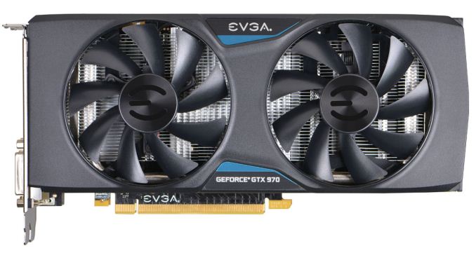
For today’s launch NVIDIA will be doing a reference launch of the GTX 980, so reference cards will be well represented while production of customized cards ramps up. Meanwhile GTX 970 is a pure virtual launch, meaning there will not be any reference cards at all. NVIDIA’s partners will be launching with customized designs right away, many of which will be carried over from their GTX 600/700 card designs. This will be a hard launch and cards should be readily available, and while NVIDIA should have no problem producing GM204 GPUs on the very mature TSMC 28nm process, it is difficult to predict just how well supplies will hold out.
On the competitive basis NVIDIA’s direct competition for the GTX 980 and GTX 970 will be split. GTX 980 is an immediate challenger for the Radeon R9 290X, AMD’s flagship single-GPU card which outside of a couple of sales continues to be priced around $499. GTX 970’s competition meanwhile will be split between the Radeon R9 290 and Radeon R9 280X. From a performance perspective the R9 290 is going to be the closer competitor, though it's priced around $399. Meanwhile the R9 280X will undercut the GTX 970 at around $279, but with much weaker performance.
NVIDIA for their part will not be running any promotions or bundles for the GTX 900 series, so what you see is what you get. Otherwise AMD will have their continuing Never Settle Forever bundle in play, which offers up to 3 free games in order to add value to the overall product.
Finally, there will be price cuts for the GTX 700 series. Officially GTX 760 stays in production with a new MSRP of $219. Meanwhile GTX 770, GTX 780, and GTX 780 Ti will go on clearance sale at whatever prices retailers can manage, and are still part of NVIDIA’s Borderlands bundle offer. That said, from a performance and power efficiency angle, the GTX 900 series is going to be a much more desirable product line.
| Fall 2014 GPU Pricing Comparison | |||||
| AMD | Price | NVIDIA | |||
| Radeon R9 295X2 | $1000 | ||||
| $550 | GeForce GTX 980 | ||||
| Radeon R9 290X | $500 | ||||
| Radeon R9 290 | $400 | ||||
| $330 | GeForce GTX 970 | ||||
| Radeon R9 280X | $280 | ||||
| Radeon R9 285 | $250 | ||||
| Radeon R9 280 | $220 | GeForce GTX 760 | |||
Meet the GeForce GTX 980
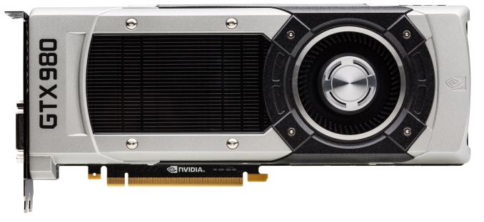
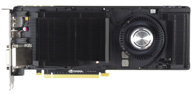
For the physical design of the reference GeForce GTX 980, NVIDIA is clearly iterating on previous designs rather than coming up with something from scratch. With that said however, the idiom of “if it ain’t broke, don’t fix it” has been very applicable to NVIDIA over the last year and a half since the launch of the GTX Titan and its high-end cooler. The GTX Titan’s cooler set a new bar in build quality and performance for a blower design that is to this day unmatched, and for that reason NVIDIA has reused this design for the GTX 780, GTX 780 Ti, GTX Titan Black, and now the GTX 980. What this means for the GTX 980 is that its design comes from a very high pedigree, one that we believe shall serve it well.
At a high level, GTX 980 recycles the basic cooler design and aesthetics of GTX 780 Ti and GTX Titan Black. This means we’re looking at a high performance blower design that is intended to offer the full heat-exhaustion benefits of a blower, but without the usual tradeoff in acoustics. The shroud of the card is composed of cast aluminum housing and held together using a combination of rivets and screws. NVIDIA has also kept the black accenting first introduced by its predecessors, giving the card distinct black lettering and a black tinted polycarbonate window. The card measures 10.5” long overall, which again is the same length as the past high-end GTX cards.
Cracking open the card and removing the shroud exposes the card’s fan and heatsink assembly. Once again NVIDIA is lining the entire card with an aluminum baseplate, which provides heatsinking capabilities for the VRMs and other discrete components below it, along with providing additional protection for the board. The primary GPU heatsink is fundamentally the same as before, retaining the same wedged shape and angled fins.
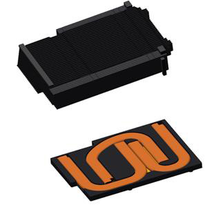
However in one of the only major deviations from the earlier GTX Titan cooler, at the base NVIDIA has dropped the vapor chamber design for a simpler (and admittedly less effective) heatpipe design that uses a trio of heatpipes to transfer heat from the GPU to the heatsink. In the case of the GTX Titan and other GK110 cards a vapor chamber was deemed necessary due to the GPU’s 250W TDP, but with GM204’s much lower 165W TDP, the advanced performance of the vapor chamber should not be necessary. We would of course like to see a vapor chamber here anyhow, but we admittedly can’t fault NVIDIA for going without it on such a low TDP part.
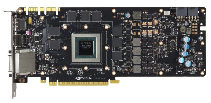
Drilling down to the PCB, we find a PCB design not all that far removed from NVIDIA’s GK110 PCBs. At the heart of the card is of course the new GM204 GPU, which although some 150mm2 smaller than GK110, is still a hefty GPU on its own. Paired with this GPU are the 8 4Gb 7GHz Samsung GDDR5 modules that surround it, composing the 4GB of VRAM and 256-bit memory bus that GM204 interfaces with.
Towards the far side of the PCB we find the card’s power delivery components, which is composed of a 4+1 phase design. Here NVIDIA is using 4 power phases for the GPU itself, and then another phase for the GDDR5. Like the 5+1 phase design on GK110 cards, this configuration is more than enough for stock operations and mild overclocking, however hardcore overclockers will probably end up gravitating towards custom designs more with more heavily overbuilt power delivery systems. Though it is interesting to note that NVIDIA’s design has open pads for 2 more power phases, meaning there is some kind of headroom left in the PCB design. Meanwhile feeding the power delivery system is a pair of 6pin PCIe sockets, giving the card a combined power delivery ceiling of 225W, which is still well above the maximum TDP NVIDIA allows for this card.
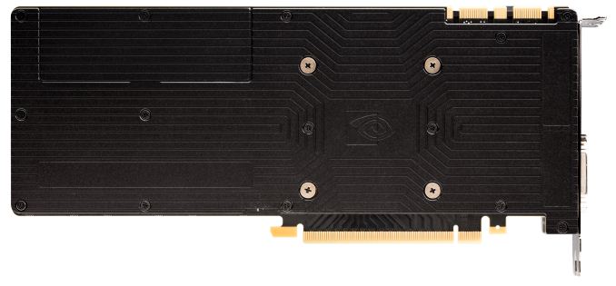
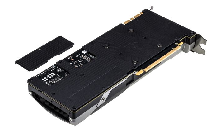
What may be the most interesting – or at least most novel – aspect of GTX 980 isn’t even found on the front side of the card, but rather it’s what’s found on the back side. Back after a long absence is a backplate for the card, which runs the entire length of the card and completely covers the back side of the PCB, leaving no element exposed except for the SLI connectors above it and the PCIe connector below it.
Generally speaking backplates are nice to have on video cards. Though they don’t provide any kind of meaningful mechanical/thermal benefit, they do serve to protect a card by reducing how much of the relatively vulnerable PCB is exposed, and similarly protect the user by keeping them from getting jabbed by the soldered tips of discrete components. However backplates typically come with one very big drawback, which is that the 2mm or so of space they occupy is not really their space, and encroaches on anything above it. For a single video card this is not a concern, but when pairing up video cards for SLI, if the cards are directly next to each other this extra 2mm makes all the difference in the world for cooling, blocking valuable space for airflow and otherwise suffocating the card unlucky enough to get blocked.
In more recent years motherboard manufacturers have done a better job of designing their boards by avoiding placing the best PCIe x16 slots next to each other, but there are still cases where these cards must be packed tightly together, such as in micro-ATX cases and when utilizing tri/quad-SLI. As a result of this clash between the benefits and drawbacks of the backplate, for GTX 980 NVIDIA has engineered a solution that allows them to include a backplate and simultaneously not impede the airflow of closely packed cards, and that is a partially removable backplate.
For GTX 980 a segment of the backplate towards the top back corner is detachable from the rest, and removing it exposes the PCB underneath. Based on studying the airflow of video cards with and without a backplate, NVIDIA tells us that they have been able to identify what portion of the backplate is responsible for impeding most of the airflow in an SLI configuration, and that they in turn have made this segment removable so as to be able to offer the full benefits of a backplate while also mitigating the airflow problems. Interestingly this segment is actually quite small – it’s only 34mm tall – making it much shorter than the radial fan on the front of the card, but NVIDIA tells us that this is all that needs to be removed to let a blocked card breathe. In our follow-up to the GTX 980 next week we will be looking at SLI performance, and this will include measuring the cooling impact of the removable backplate segment.
Moving on, beginning with GTX 980 NVIDIA’s standard I/O configuration has dramatically changed, and so for that matter has the design of their I/O shield. First introduced with GTX Titan Z and now present on GTX 980, NVIDIA has been working to maximize the amount of airflow available through their I/O bracket by replacing standard rectangular vents with triangular vents across the whole card. This results in pretty much every square centimeter of the card not occupied by an I/O port having venting through it, leading to very little of the card actually being blocked by the I/O shield.
Meanwhile starting with GTX 980, NVIDIA is introducing their new standard I/O configuration. NVIIDA has finally dropped the second DL-DVI port, and in its place they have installed a pair of full size DisplayPorts. This brings the total I/O configuration up to 1x DL-DVI-I, 3x DisplayPort 1.2, and 1x HDMI 2.0. The inclusion of more DisplayPorts has been a long time coming and I’m glad to see that NVIDIA has finally gone this route. DisplayPorts offer more functionality than any other type of port and can easily be converted to HDMI or SL-DVI as necessary. More importantly for NVIDIA, with 3 DisplayPorts NVIDIA can now drive 3 G-Sync monitors off of a single card, making G-Sync Surround viable for the first time.
Speaking of I/O, we’ll briefly note that NVIDIA’s SLI connectors are still present, with the pair of connectors allowing up to quad-SLI. However we’d also note that this also means that for anyone hoping that NVIDIA would have an all-PCIe multi-GPU solution analogous to AMD’s XDMA engine, Maxwell 2 will not be such a product. Physical bridges are still necessary for SLI, with NVIDIA splitting up the workload over SLI and PCIe in the case of very high resolutions such as 4K.
Wrapping up our look at the physical build quality of the GTX 980, NVIDIA has done a good job iterating on what was already an excellent design with the GTX Titan and its cooler. The backplate, though not a remarkable difference, does give the card that last bit of elegance that GTX Titan and its GK110 siblings never had, as the card is now clad in metal from top to bottom. As silly as it sounds, other than the PCIe connector the GTX 980 may as well be a complete consumer electronic product of its own, as it’s certainly built like one.
Finally, along with the hardware we also want to quickly summarize the GPU Boost 2.0 limits NVIDIA has chosen for the GTX 980, to better illustrate what the card is capable of. Like the other high-end NVIDIA cards before it, NVIDIA has opted to set the GTX 980’s temperature target at 80C, with a maximum target of 91C and an absolute thermal threshold of 95C. Meanwhile the card’s 165W TDP limit can be increased by as much as 25% to 206W, or 41W over its reference limit.
It’s interesting to note that despite the fact that the GTX Titan cooler was designed for a 250W card, GTX 980 will still see some temperature throttling under heavy, sustained loads. NVIDIA seems to have invested most of their cooling gains into acoustics, which has produced a card with amazing acoustic performance given the combination of the blower and the chart-topping performance, but it has also produced a card that is still going to throttle from time to time.
The Test
For the launch of GTX 980 we are using NVIDIA’s press beta drivers for the card, release 334.07 beta. This is the first (semi) public release of the R343 driver set, and coinciding with the release of the Maxwell 2 architecture it also marks the end of support for NVIDIA’s D3D10 GPUs: the 8, 9, 100, 200, and 300 series. Beginning with R343 these products are no longer supported in new driver branches and have been moved to legacy status.
Meanwhile as noted earlier, due to time constraints and hardware problems today we are focusing our coverage on the GTX 980. Next week we will be looking at GTX 980 SLI (hint: it’s fast) and GTX 970.
And on a testing note, as is standard for our reviews we are using our reference Radeon R9 290X for our 290X benchmarks. For this reason we are including both the standard and uber modes for the sake of clarity and completeness. The temperature throttling that the reference 290X suffers from is basically limited to just the reference 290X, as the non-reference/custom models use open air coolers that have no problem dissipating the 290X’s full heat load. Both modes are included for this reason, to demonstrate how a reference 290X performs and how a custom model would perform. At this point you can still buy reference 290X cards, but the vast majority of retail cards will be of the non-reference variety, where the 290X Uber mode’s results will be more applicable.
| CPU: | Intel Core i7-4960X @ 4.2GHz |
| Motherboard: | ASRock Fatal1ty X79 Professional |
| Power Supply: | Corsair AX1200i |
| Hard Disk: | Samsung SSD 840 EVO (750GB) |
| Memory: | G.Skill RipjawZ DDR3-1866 4 x 8GB (9-10-9-26) |
| Case: | NZXT Phantom 630 Windowed Edition |
| Monitor: | Asus PQ321 |
| Video Cards: |
AMD Radeon R9 290X AMD Radeon R9 290 AMD Radeon HD 7970 AMD Radeon HD 6970 NVIDIA GeForce GTX 980 NVIDIA GeForce GTX 780 Ti NVIDIA GeForce GTX 780 NVIDIA GeForce GTX 770 NVIDIA GeForce GTX 680 NVIDIA GeForce GTX 580 |
| Video Drivers: |
NVIDIA Release 344.07 Beta AMD Catalyst 14.300.1005 Beta |
| OS: | Windows 8.1 Pro |
Metro: Last Light
As always, kicking off our look at performance is 4A Games’ latest entry in their Metro series of subterranean shooters, Metro: Last Light. The original Metro: 2033 was a graphically punishing game for its time and Metro: Last Light is in its own right too. On the other hand it scales well with resolution and quality settings, so it’s still playable on lower end hardware.
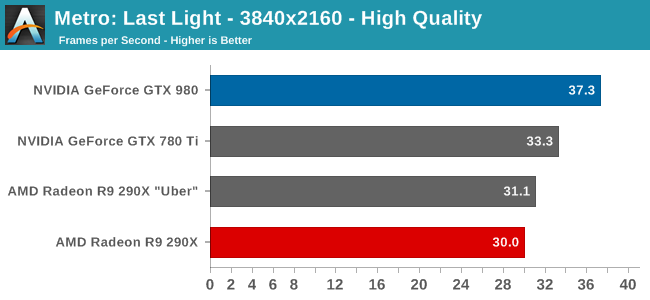
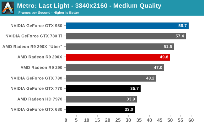
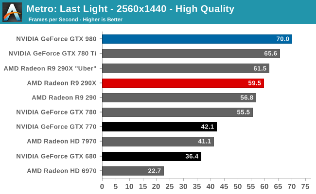
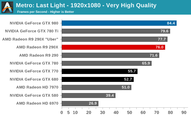
As has become customary for us for the last couple of high-end video card reviews, we’re going to be running all of our 4K video card benchmarks at both high quality and at a lower quality level. In practice not even GTX 980 is going to be fast enough to comfortably play most of these games at 3840x2160 with everything cranked up – that is going to be multi-GPU territory – so for that reason we’re including a lower quality setting to showcase just what performance looks like at settings more realistic for a single GPU.
GTX 980 comes out swinging in our first set of benchmarks. If there was any doubt that it could surpass the likes of R9 290XU and GTX 780 Ti, then this first benchmark is a great place to set those doubts to rest. At all resolutions and quality settings it comes out on top, surpassing NVIDIA’s former consumer flagship by anywhere from a few percent to 12% at 4K with high quality settings. Otherwise against the R9 290XU it’s a consistent 13% lead at 2560 and 4K Medium.
In absolute terms this is enough performance to keep its average framerates well over 60fps at 2560, and even at 3840 Medium it comes just short of crossing the 60fps mark. High quality mode will take the wind out of GTX 980’s sails though, pushing framerates back into the borderline 30fps range.
Looking at NVIDIA’s last-generation parts for a moment, the performance gains over the lower tier GK110 based GTX 780 are around 25-35%. This is about where you’d expect to see a new GTX x80 card given NVIDIA’s quasi-regular 2 year performance upgrade cadence. And when extended out to a full 2 years, the performance advantage over GTX 680 is anywhere between 60% and 92% depending on the resolution we’re looking at. NVIDIA proclaims that GTX 980 will achieve 2x the performance per watt of GTX 680, and since GTX 980 is designed to operate at a lower TDP than GTX 680, as we can see it means performance over GTX 680 won’t quite be doubled in most cases.
Company of Heroes 2
Our second benchmark in our benchmark suite is Relic Games’ Company of Heroes 2, the developer’s World War II Eastern Front themed RTS. For Company of Heroes 2 Relic was kind enough to put together a very strenuous built-in benchmark that was captured from one of the most demanding, snow-bound maps in the game, giving us a great look at CoH2’s performance at its worst. Consequently if a card can do well here then it should have no trouble throughout the rest of the game.
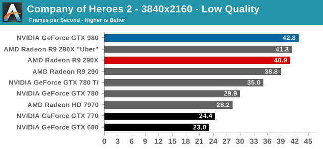
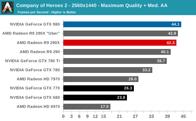
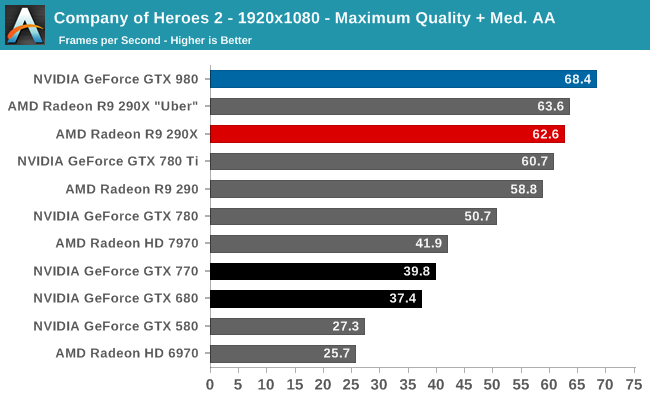
Since CoH2 is not AFR compatible, the best performance you’re going to get out of it is whatever you can get out of a single GPU. In which case the GTX 980 is the fastest card out there for this game. AMD’s R9 290XU does hold up well though; the GTX 980 may have a lead, but AMD is never more than a few percent behind at 4K and 1440p. The lead over the GTX 780 Ti is much more substantial on the other hand at 13% to 22%. So NVIDIA has finally taken this game back from AMD, as it were.
Elsewhere against the GTX 680 this is another very good performance for the GTX 980, with a performance advantage over 80%.
On an absolute basis, at these settings you’re looking at an average framerate in the 40s, which for an RTS will be a solid performance.
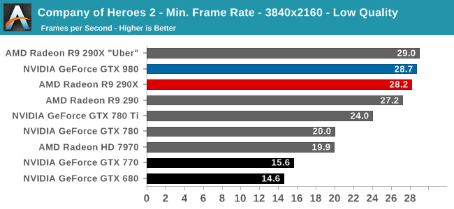
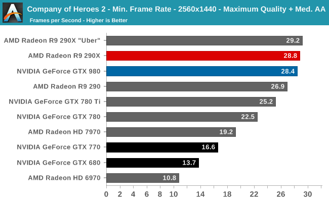
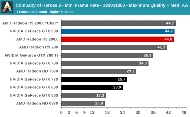
However when it comes to minimum framerates, GTX 980 can’t quite stay on top. In every case it is ever so slightly edged out by the R9 290XU by a fraction of a frame per second. AMD seems to weather the hardest drops in framerates just a bit better than NVIDIA does. Though neither card can quite hold the line at 30fps at 1440p and 4K.
Bioshock Infinite
Bioshock Infinite is Irrational Games’ latest entry in the Bioshock franchise. Though it’s based on Unreal Engine 3 – making it our obligatory UE3 game – Irrational had added a number of effects that make the game rather GPU-intensive on its highest settings. As an added bonus it includes a built-in benchmark composed of several scenes, a rarity for UE3 engine games, so we can easily get a good representation of what Bioshock’s performance is like.
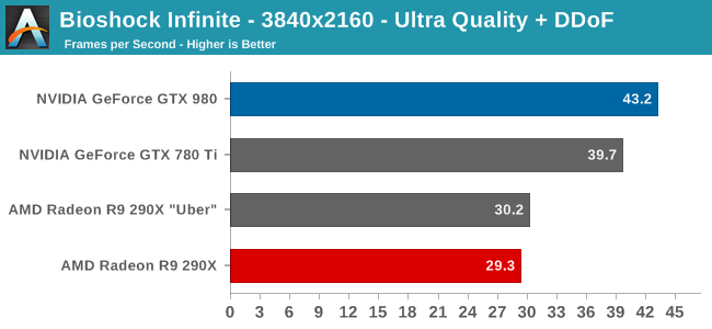
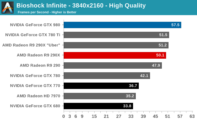
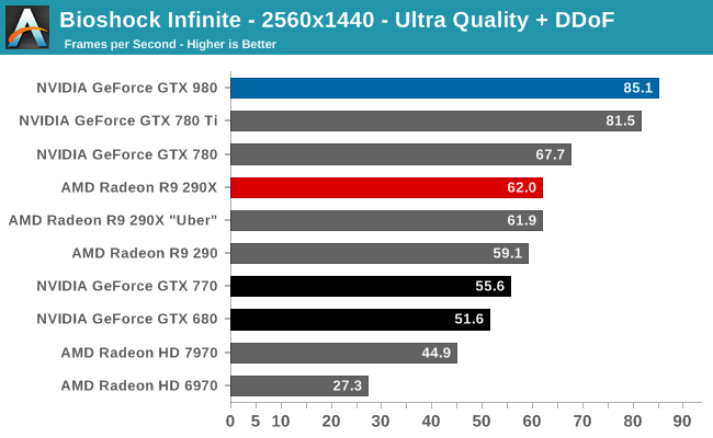
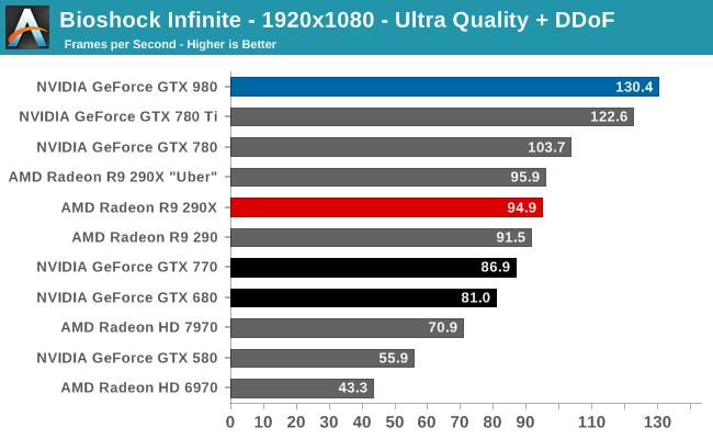
Even with advanced depth of field effects, our highest end video cards are starting to run away with Bioshock: Infinite. That is particularly true for the GTX 980, which in a game that NVIDIA frequently does well in further props up the GTX 980’s advantage. Only at 4K are the R9 290XU and GTX 980 anywhere near close, otherwise at 1440p it’s a 37% performance advantage. GTX 780 Ti on the other hand holds much closer, still falling behind the GTX 980 but only by around 5% at sub-4K resolutions. This does make for a good moment for showcasing the GTX 980’s greater ROP throughput though; as we crank up the resolution to 4K, the 780 Ti falls further behind, especially when we’re at lower quality settings that leave us less shader-bound.
On an absolute basis 120Hz/144Hz gamer should have a blast even with a single GTX 980 at 1080p, while purists will need more performance for 1440p than the 85fps the card can offer. And at 4K the GTX 980 is doing very well for itself, almost cracking 60fps at High quality, and becoming the only card to crack 40fps with Ultra quality.
This will be one of the weaker showings for the GTX 980 over the GTX 680 though; at sub-4K resolutions it’s only a 60-65% performance improvement.


Meanwhile Bioshock is the first of 5 games we can reliably measure with the FCAT tools to check for frame pacing consistency. Bioshock is a bit more erratic than most games in this respect, and while our general rule of thumb for an excellent performance from a single card is 3%, our recording for GTX 980 is a bit higher at 3.5%. On the other hand at 4K it measures in at just 2.3%. So while frame pacing is going to be a bit of a rubber stamping process overall, we can confirm that GTX 980 is delivering a good frame pacing experience in Bioshock.
Battlefield 4
Our latest addition to our benchmark suite and our current major multiplayer action game of our benchmark suite is Battlefield 4, DICE’s 2013 multiplayer military shooter. After a rocky start, Battlefield 4 has finally reached a point where it’s stable enough for benchmark use, giving us the ability to profile one of the most popular and strenuous shooters out there. As these benchmarks are from single player mode, based on our experiences our rule of thumb here is that multiplayer framerates will dip to half our single player framerates, which means a card needs to be able to average at least 60fps if it’s to be able to hold up in multiplayer.
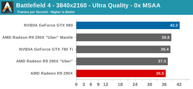
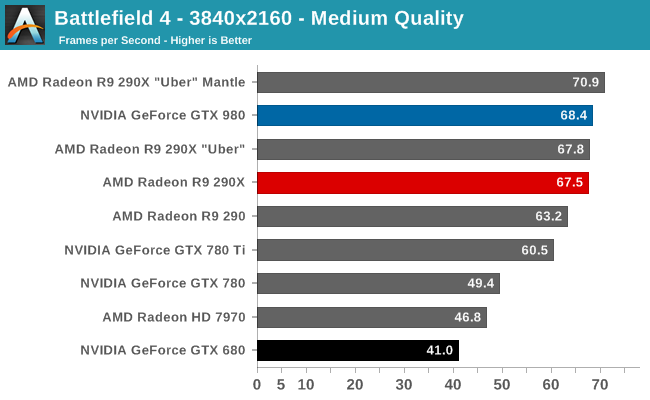
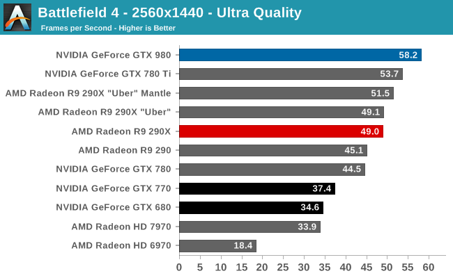
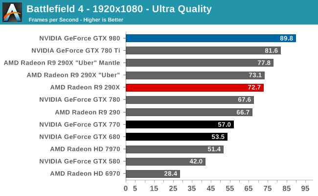
Battlefield 4 is one of our tougher games, especially with the bar set at 60fps to give us enough headroom for multiplayer performance. To that end the GTX 980 turns in another solid performance, though the dream of averaging 60fps at 1440p Ultra is going to have to wait just a bit longer to be answered.
Overall on a competitive basis the GTX 980 looks very strong. Against the GTX 780 Ti it further improves on performance by 8-13%, 30%+ against GTX 780, and 66% against GTX 680. Similarly it fares well against AMD’s cards – even with their Mantle performance advantage – with the exception of one case: 4K at Medium quality. With maximum quality settings, at all resolutions the GTX 980 can outperform AMD’s best by around 15%. But in the case of 4K Medium, with the lesser shader overhead in particular the R9 290XU gets to pull ahead thanks to Mantle. At this point NVIDIA is losing by just 4%, but it goes to show how close the race between these two cards is going to be at times and why AMD is never too far behind NVIDIA in several of these games.
In any case for Ultra quality you’re looking at the GTX 980 being enough for 1080p and even 1440p if you flex the 60fps rule a bit. 4K at these settings though is going to be the domain of multi-GPU setups.


Meanwhile delta percentage performance is extremely strong here. Everyone, incuding the GTX 980, is well below 3%.
Crysis 3
Still one of our most punishing benchmarks, Crysis 3 needs no introduction. With Crysis 3, Crytek has gone back to trying to kill computers and still holds “most punishing shooter” title in our benchmark suite. Only in a handful of setups can we even run Crysis 3 at its highest (Very High) settings, and that’s still without AA. Crysis 1 was an excellent template for the kind of performance required to drive games for the next few years, and Crysis 3 looks to be much the same for 2014.
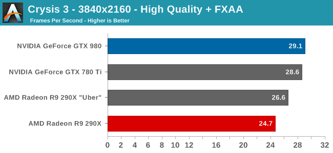
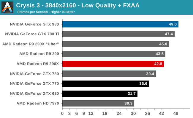
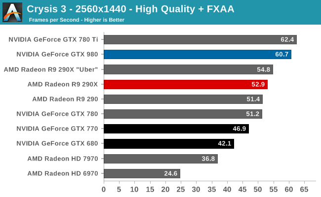
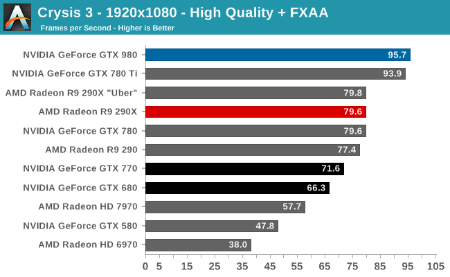
Meanwhile delta percentage performance is extremely strong here. Everyone, including the GTX 980, is well below 3%.
Always a punishing game, Crysis 3 ends up being one of the only games the GTX 980 doesn’t take a meaningful lead on over the GTX 780 Ti. To be clear the GTX 980 wins in most of these benchmarks, but not in all of them, and even when it does win the GTX 780 Ti is never far behind. For this reason the GTX 980’s lead over the GTX 780 Ti and the rest of our single-GPU video cards is never more than a few percent, even at 4K. Otherwise at 1440p we’re looking at the tables being turned, with the GTX 980 taking a 3% deficit. This is the only time the GTX 980 will lose to NVIDIA’s previous generation consumer flagship.
As for the comparison versus AMD’s cards, NVIDIA has been doing well in Crysis 3 and that extends to the GTX 980 as well. The GTX 980 takes a 10-20% lead over the R9 290XU depending on the resolution, with its advantage shrinking as the resolution grows. During the launch of the R9 290 series we saw that AMD tended to do better than NVIDIA at higher resolutions, and while this pattern has narrowed some, it has not gone away. AMD is still the most likely to pull even with the GTX 980 at 4K resolutions, despite the additional ROPS available to the GTX 980.
This will also be the worst showing for the GTX 980 relative to the GTX 680. GTX 980 is still well in the lead, but below 4K that lead is just 44%. NVIDIA can’t even do 50% better than the GTX 680 in this game until we finally push the GTX 680 out of its comfort zone at 4K.
All of this points to Crysis 3 being very shader limited at these settings. NVIDIA has significantly improved their CUDA core occupancy on Maxwell, but in these extreme situations GTX 980 will still struggle with the CUDA core deficit versus GK110, or the limited 33% increase in CUDA cores versus GTX 680. Which is a feather in Kepler’s cap if anything, showing that it’s not entirely outclassed if given a workload that maps well to its more ILP-sensitive shader architecture.


The delta percentage story continues to be unremarkable with Crysis 3. GTX 980 does technically fare a bit worse, but it’s still well under 3%. Keep in mind that delta percentages do become more sensitive at higher framerates (there is less absolute time to pace frames), so a slight increase here is not unexpected.
Crysis: Warhead
Up next is our legacy title for 2014, Crysis: Warhead. The stand-alone expansion to 2007’s Crysis, at over 5 years old Crysis: Warhead can still beat most systems down. Crysis was intended to be future-looking as far as performance and visual quality goes, and it has clearly achieved that. We’ve only finally reached the point where single-GPU cards have come out that can hit 60fps at 1920 with 4xAA, never mind 2560 and beyond.
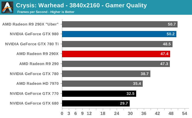
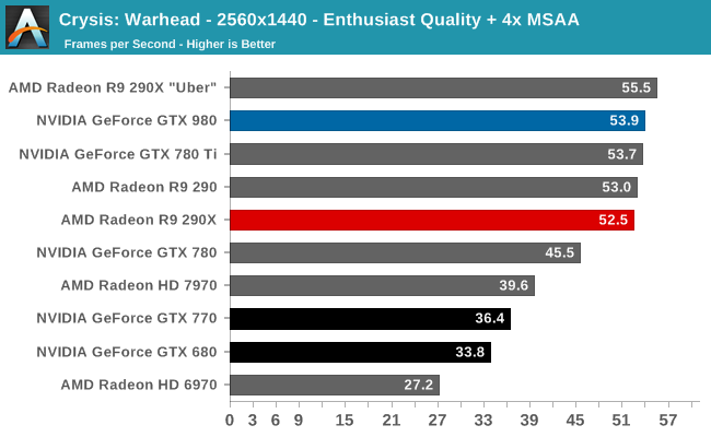
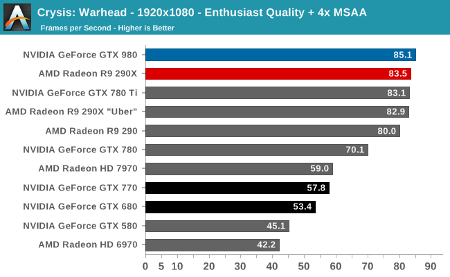
At the launch of the GTX 680, Crysis: Warhead was rather punishing of the GTX 680’s decreased memory bandwidth versus GTX 580. The GTX 680 was faster than the GTX 580, but the gains weren’t as great as what we saw elsewhere. For this reason the fact that the GTX 980 can hold a 60% lead over the GTX 680 is particularly important because it means that NVIDIA’s 3rd generation delta color compression is working and working well. This has allowed NVIDIA to overcome quite a bit of memory bandwidth bottlenecking in this game and push performance higher.
That said, since GTX 780 Ti has a full 50% more memory bandwidth, it’s telling that GTX 780 Ti and GTX 980 are virtually tied in this benchmark. Crysis: Warhead will gladly still take what memory bandwidth it can get from NVIDIA cards.
Otherwise against AMD cards this is the other game where GTX 980 can’t cleanly defeat R9 290XU. These cards are virtually tied, with AMD edging out NVIDIA in two of three tests. Given their differing architectures I’m hesitant to say this is a memory bandwidth factor as well, but if it were then R9 290XU has a very big memory bandwidth advantage going into this.
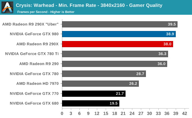
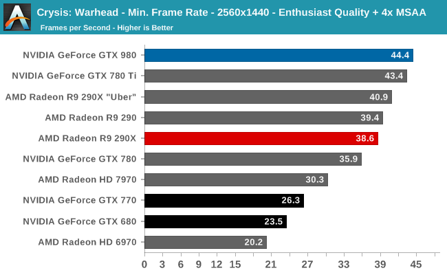
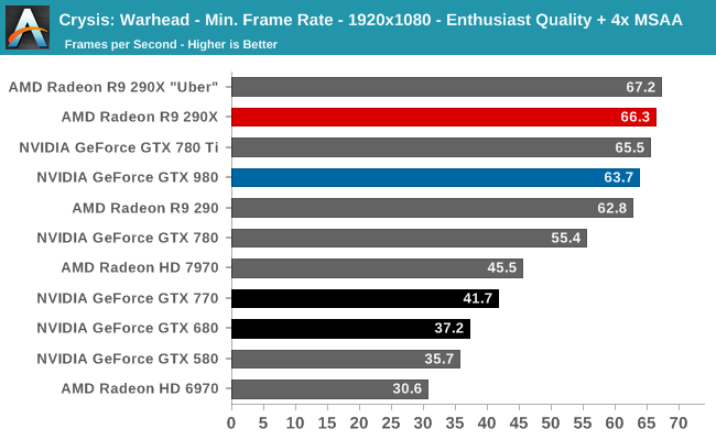
When it comes to minimum framerates the story is much the same, with the GTX 980 and AMD trading places. Though it’s interesting to note that the GTX 980 is doing rather well against the GTX 680 here; that memory bandwidth advantage would appear to really be paying off with minimum framterates.
Total War: Rome 2
The second strategy game in our benchmark suite, Total War: Rome 2 is the latest game in the Total War franchise. Total War games have traditionally been a mix of CPU and GPU bottlenecks, so it takes a good system on both ends of the equation to do well here. In this case the game comes with a built-in benchmark that plays out over a forested area with a large number of units, definitely stressing the GPU in particular.
For this game in particular we’ve also gone and turned down the shadows to medium. Rome’s shadows are extremely CPU intensive (as opposed to GPU intensive), so this keeps us from CPU bottlenecking nearly as easily.
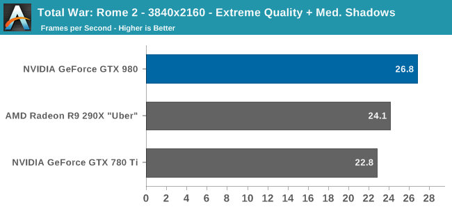
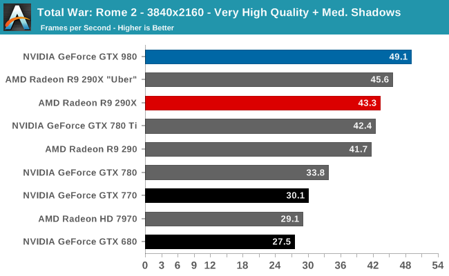
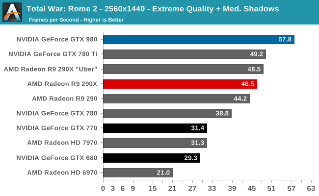
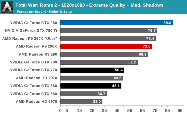
Of all of our games, there is no better set of benchmarks for the GTX 980 than Total War: Rome II. Against both AMD and NVIDIA’s last-generation cards it never wins by as much as it wins here.
Compared to the GTX 780 Ti the GTX 980 is a consistent 16-17% ahead at all resolutions. Meanwhile against the R9 280XU this is an 18% lead at 1080p and 1440p. R9 290XU only begins to catch up at 4K Very High quality, where GTX 980 still leads by a respectable 8%.
This is also a very strong showing compared to the GTX 680. The overall lead is 80-95% depending on the resolution. The GTX 980 was not necessarily meant to double the GTX 680’s performance, but it comes very close to doing so here at 1440p.
Given what happens to the GK104 cards in this game, I suspect we’re looking at the results of either the ROP advantage and/or a very good case CUDA core occupancy improvements. The fact that the lead over the GTX 780 Ti is so consistent over all resolutions does point to the CUDA core theory, but we can’t really rule out the ROPs with the information we have.
As for results on an absolute basis, not even mighty GTX 980 is going to crack 30fps at 4K with Extreme settings. In lieu of that Very High quality comes off quite well at 49fps, and we’re just shy of hitting 60fps at 1440p with Extreme.
Thief
Our latest addition to our benchmark suite is Eidos Monreal’s stealth action game, Thief. Set amidst a Victorian-era fantasy environment, Thief is an Unreal Engine 3 based title which makes use of a number of supplementary Direct3D 11 effects, including tessellation and advanced lighting. Adding further quality to the game on its highest settings is support for SSAA, which can eliminate most forms of aliasing while bringing even the most powerful video cards to their knees.
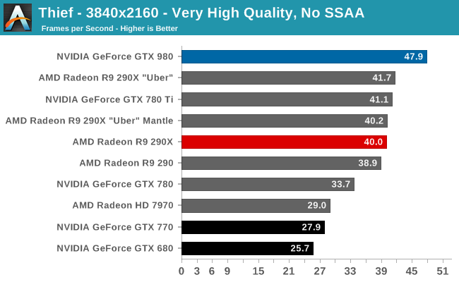
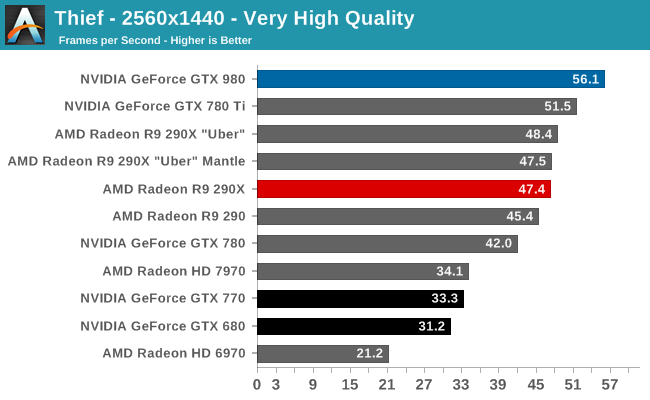
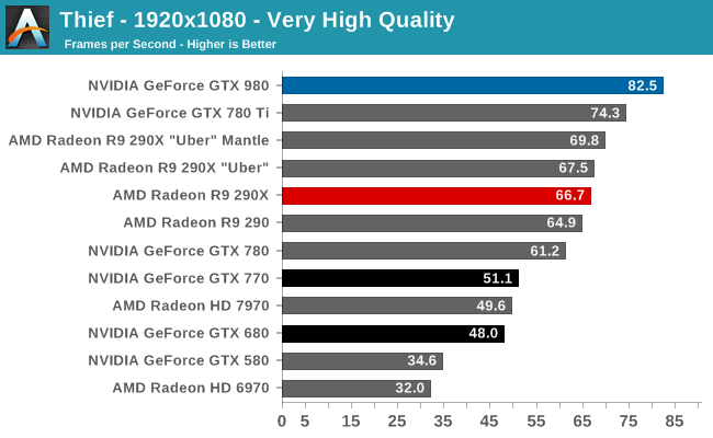
Thief is another solid win for the GTX 980. The closest anyone gets to it is within 10%, and the lead only widens from there. Against the GTX 780 Ti, this is a lead of anywhere between 10% and 16%, and against the R9 290 XU it’s 15-22%; Mantle doing the card no favors for average framerates above 1080p.
The performance advantage over the GTX 780 and GTX 680 is also above average. GTX 980 can outrun the previous x80 card by 33% or more, and the GTX 680 by at least 80%.
On an absolute basis the GTX 980 won’t quite crack 60fps at 1440p, but it does come very close at 56fps. And since thief is running an internal form of SSAA, turning up the resolution to 4K and dropping the SSAA still yields playable framerates, though at 48fps it’s closer to 45 than 60. 60fps is going to require a bit more horsepower than what a single GTX 980 can deliver today.
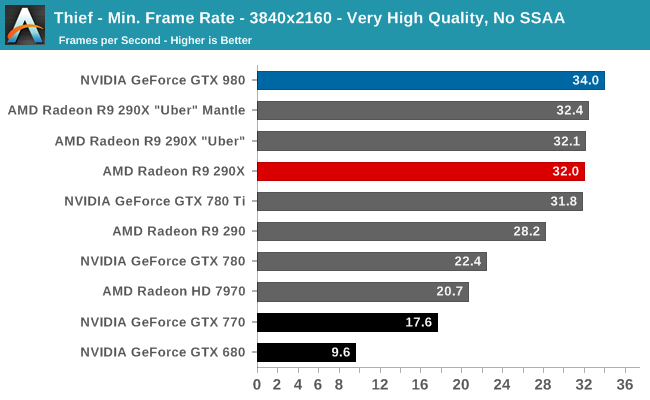
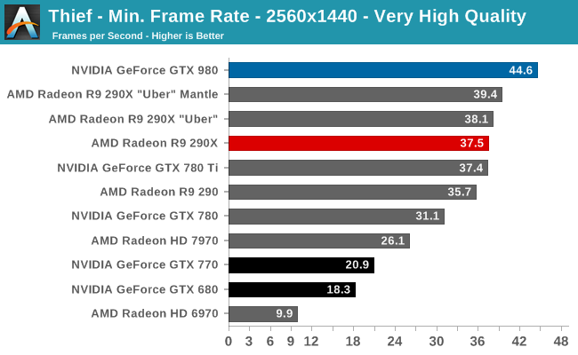
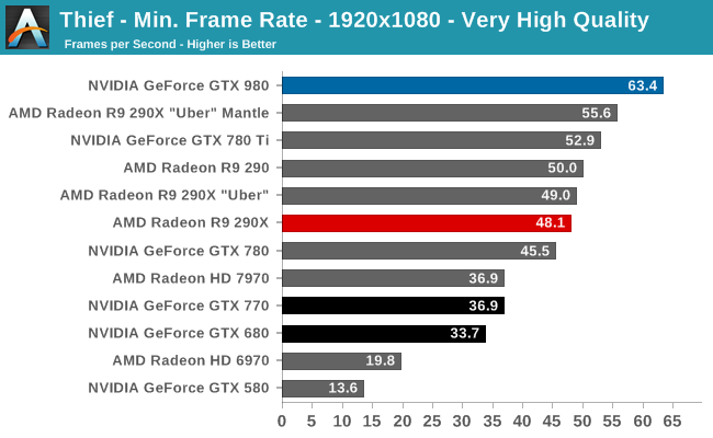
The GTX 980’s performance advantage generally holds up when it comes to minimum framerates as well. Though it is interesting to note that until we get to 4K, the GTX 980 holds a larger minimum framerate advantage over the GTX 780 Ti than it does an average framerate advantage – 20% verus about 10%. On the other hand the use of Mantle begins to close the gap for the R9 290XU a bit, but it’s still not enough to make up for the GTX 980’s strong overall performance advantage, especially at 1080p.


Our delta percentages are once more unremarkable. All cards are consistently below 3% here.
GRID 2
The final game in our benchmark suite is also our racing entry, Codemasters’ GRID 2. Codemasters continues to set the bar for graphical fidelity in racing games, and with GRID 2 they’ve gone back to racing on the pavement, bringing to life cities and highways alike. Based on their in-house EGO engine, GRID 2 includes a DirectCompute based advanced lighting system in its highest quality settings, which incurs a significant performance penalty but does a good job of emulating more realistic lighting within the game world.
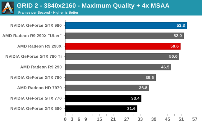
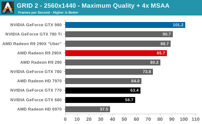
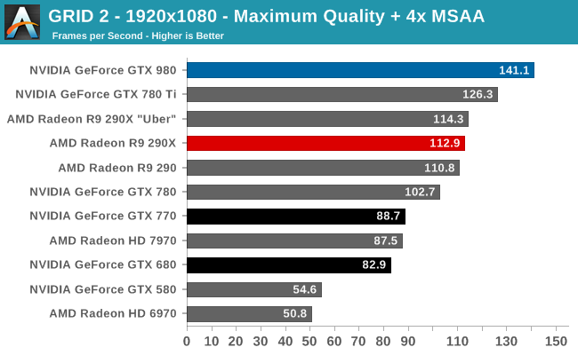
Our final game is another solid victory for the GTX 980. The GTX 980’s lead does shrink at 4K, otherwise we’re looking at a 12% advantage over the GTX 780 Ti and 14-23% over R9 290XU.
144Hz gamers will find 1080p quite useful, with the GTX 980 coming just short of averaging a matching framerate. Otherwise for 2560p one would need to settle for 101fps. Though for 4K gamers, even a single GTX 980 is more or less enough here; 53fps at 4K with Maximum quality and 4x MSAA means that at most a drop to 2x MSAA would get it above 60fps without involving a second card. Maybe this is a good case for NVIDIA’s new Multi-Frame sampled Anti-Aliasing?
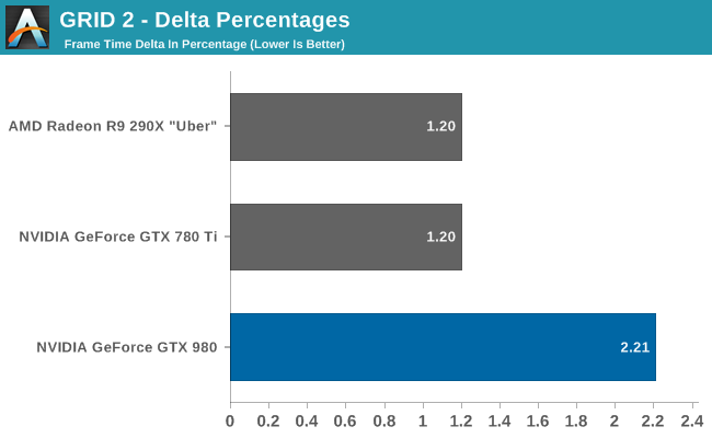
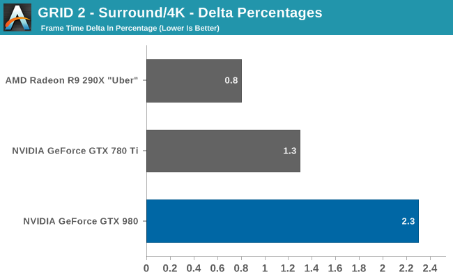
Our last set of delta percentages once again finds the GTX 980 easily below 3%. Though the variance is higher than with the other two cards, and by more than just what we would expect as a result of higher average framerates.
Synthetics
As always we’ll also take a quick look at synthetic performance. These tests mainly serve as a canary for finding important architectural changes, and with the exception of pixel throughput we are not expecting any major changes for GTX 980 and GM204.
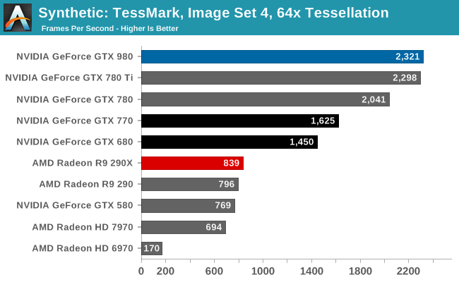
GM204 is designed to have an ever-so-slightly higher triangle throughput rate than GK110 – 16 tris/clock versus 15 tris/clock, and sure enough the GTX 980 comes out on top in TessMark, slightly edging out the GTX 780 Ti. The difference is only very slight here, and though GM204 should be a bit more powerful than GK110 in practice it’s a dead heat.
Moving on, we have our 3DMark Vantage texture and pixel fillrate tests, which present our cards with massive amounts of texturing and color blending work. These aren’t results we suggest comparing across different vendors, but they’re good for tracking improvements and changes within a single product family.
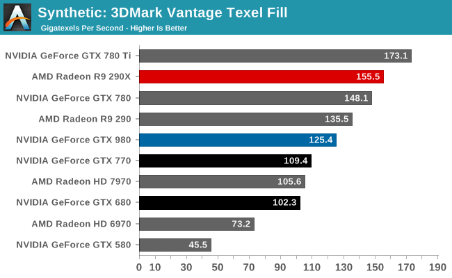
Beginning with Maxwell NVIDIA reduced their texture-to-compute ratio from 12:1 to 16:1. As a result of this change Maxwell GPUs have fewer texture units than comparable Kepler GPUs. Compounding this effect is the fact that Maxwell CUDA cores are more efficient than Kepler CUDA cores, leading to NVIDIA placing fewer cores overall and further reducing the texture fill rate.
As a result the GTX 980 is not texture fillrate competitive with any of the GK110 cards. It is competitive with the GK104 cards, but only because these cards had the same number of texture units at 128. NVIDIA has told us that they believe this new ratio is a better fit for modern workloads, and judging from the performance we’re seeing elsewhere it would appear that NVIDIA is right.
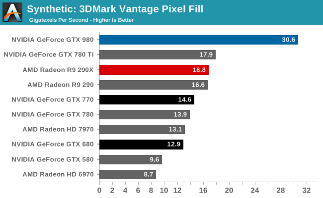
On the other hand, thanks to NVIDIA’s newer 3rd generation delta color compression technology, our 3DMark pixel fillrate performance is through the roof. GTX 980 comes very close to doubling the throughput of our GK110 cards and more than doubles the throughput of the GK104 cards, reflecting the fact that it has 64 ROPs and more importantly has the available bandwidth to put them to good use.
This benchmark in a nutshell is why NVIDIA can deliver chart-topping performance despite having only 2/3rds the memory bandwidth of GTX 780 Ti. By improving their color compression to this point, NVIDIA can significantly reduce their memory bandwidth requirements Maxwell 2, allowing them to do more with less. In real games the result won’t be anywhere near this remarkable since this is a pure pixel fillrate test, but it goes to show that NVIDIA has been able to expand their effective memory bandwidth in concert with their ROP and shader performance improvements.
Compute
On the other hand compared to our Kepler cards GTX 980 introduces a bunch of benefits. Higher CUDA core occupancy is going to be extremely useful in compute benchmarks. So will the larger L2 cache and the 96KB per SMM of shared memory. Even more important, compares to GK104 (GTX 680/770) GTX 980 inherits the compute enhancements that were introduced in GK110 (GTX 780/780 Ti) including changes that relieved pressure on register file bandwidth and capacity. So although GTX 980 is not strictly a compute card – it is first and foremost a graphics card – it has a lot of resources available to spend on compute.
As always we’ll start with LuxMark2.0, the official benchmark of SmallLuxGPU 2.0. SmallLuxGPU is an OpenCL accelerated ray tracer that is part of the larger LuxRender suite. Ray tracing has become a stronghold for GPUs in recent years as ray tracing maps well to GPU pipelines, allowing artists to render scenes much more quickly than with CPUs alone.
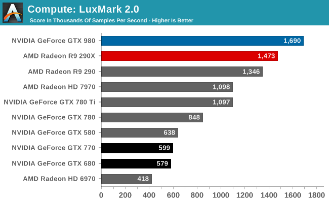
Out of the gate GTX 980 takes off like a rocket. AMD’s cards could easily best even GTX 780 Ti here, but GTX 980 wipes out AMD’s lead and then some. At 1.6M samples/sec, GTX 980 Ti is 15% faster than R9 290X and 54% faster than GTX 780 Ti. This, as it’s important to remind everyone, is for a part that technically only has 71% of the CUDA cores of GTX 780 Ti. So per CUDA core, GTX 980 delivers over 2x the LuxMark performance of GTX 780 Ti. Meanwhile against GTX 680 and GTX 780 the lead is downright silly. GTX 980 comes close to tripling its GK104 based predecessors.
I’ve spent some time pondering this, and considering that GTX 750 Ti looked very good in this test as well it’s clear that Maxwell’s architecture has a lot to do with this. I don’t know if NVIDIA hasn’t also been throwing in some driver optimizations here, but a big part is being played by parts of the architecture. GTX 750 Ti and GTX 980 both share the general architecture and 2MB of L2 cache, while it seems like we can run out GTX 980’s larger 96KB shared memory since GTX 750 Ti did not have that. This may just come down to those CUDA core occupancy improvements, especially if you start comparing GTX 980 to GTX 780 Ti.
For our second set of compute benchmarks we have CompuBench 1.5, the successor to CLBenchmark. We’re not due for a benchmark suite refresh until the end of the year, however as CLBenchmark does not know what to make of GTX 980 and is rather old overall, we’ve upgraded to CompBench 1.5 for this review.
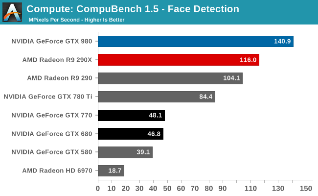
The first sub-benchmark is Face Detection, which like LuxMark puts GTX 980 in a very good light. It’s quite a bit faster than GTX 780 Ti or R9 290X, and comes close to trebling GTX 680.
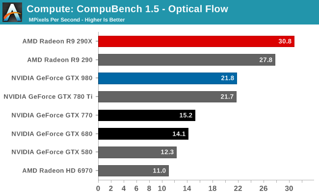
The second sub-benchmark of Optical Flow on the other hand sees AMD put GTX 980 in its place. GTX 980 fares only as well as GTX 780 Ti here, which means performance per CUDA core is up, but not enough to offset the difference in cores. And it doesn’t get GTX 980 anywhere close to beating R9 290X. As a computer vision test this can be pretty memory bandwidth intensive, so this may be a case of GTX 980 succumbing to its lack of memory bandwidth rather than a shader bottleneck.
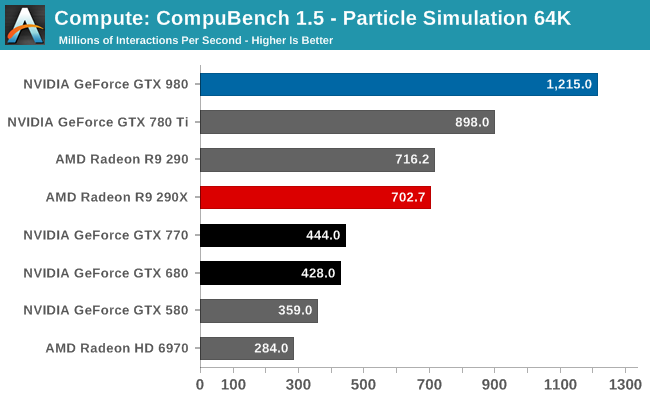
The final sub-benchmark of the particle simulation puts GTX 980 back on top, and by quite a lot. NVIDIA does well in this benchmark to start with – GTX 780 Ti is the number 2 result – and GTX 980 only improves on that. It’s 35% faster than GTX 780 Ti, 73% faster than R9 290X, and GTX 680 is nearly trebled once again. CUDA core occupancy is clearly a big part of these results, though I wonder if the L2 cache and shared memory increase may also be playing a part compared to GTX 780 Ti.
Our 3rd compute benchmark is Sony Vegas Pro 12, an OpenGL and OpenCL video editing and authoring package. Vegas can use GPUs in a few different ways, the primary uses being to accelerate the video effects and compositing process itself, and in the video encoding step. With video encoding being increasingly offloaded to dedicated DSPs these days we’re focusing on the editing and compositing process, rendering to a low CPU overhead format (XDCAM EX). This specific test comes from Sony, and measures how long it takes to render a video.
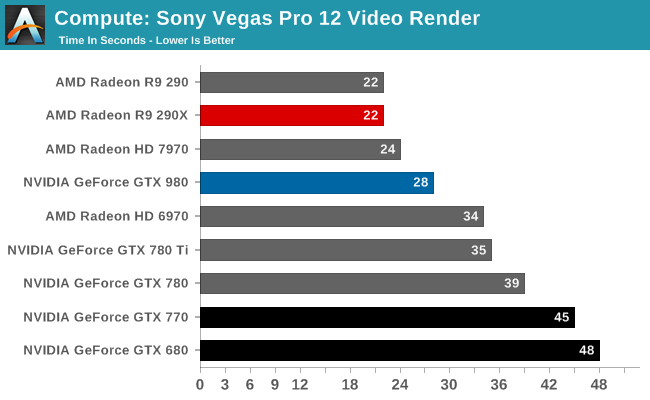
Traditionally a benchmark that favored AMD, the GTX 980 doesn’t manage to beat the R9 290X, but it closes the gap significantly compared to GTX 780 Ti. This test is a mix of simple shaders and blends, so it’s likely we’re seeing a bit of both here. More ROPs for more blending, and improved shader occupancy for when the task is shader-bound.
Moving on, our 4th compute benchmark is FAHBench, the official Folding @ Home benchmark. Folding @ Home is the popular Stanford-backed research and distributed computing initiative that has work distributed to millions of volunteer computers over the internet, each of which is responsible for a tiny slice of a protein folding simulation. FAHBench can test both single precision and double precision floating point performance, with single precision being the most useful metric for most consumer cards due to their low double precision performance. Each precision has two modes, explicit and implicit, the difference being whether water atoms are included in the simulation, which adds quite a bit of work and overhead. This is another OpenCL test, utilizing the OpenCL path for FAHCore 17.
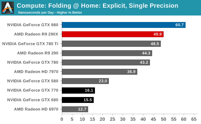
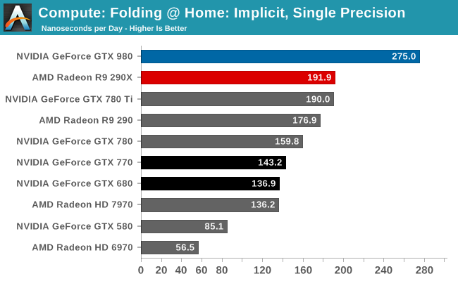
This is another success story for the GTX 980. In both single precision tests the GTX 980 comes out on top, holding a significant lead over the R9 290X. Furthermore we’re seeing some big performance gains over GTX 780 Ti, and outright massive gains over GTX 680, to the point that GTX 980 comes just short of quadrupling GTX 680’s performance in single precision explicit. This test is basically all about shading/compute, so we expect we’re seeing a mix of improvements to CUDA core occupancy, shared memory/cache improvements, and against GTX 680 those register file improvements.
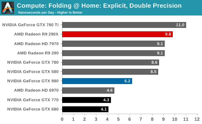
Double precision on the other hand is going to be the GTX 980’s weak point for obvious reasons. GM204 is a graphics GPU first and foremost, so it only has very limited 1:32 rate FP64 performance, leaving it badly outmatched by anything with a better rate. This includes GTX 780/780 Ti (1:24), AMD’s cards (1:8 FP64), and even ancient GTX 580 (1:8). If you want to do real double precision work, NVIDIA clearly wants you buying their bigger, compute-focused products such as GTX Titan, Quadro, and Tesla.
Wrapping things up, our final compute benchmark is an in-house project developed by our very own Dr. Ian Cutress. SystemCompute is our first C++ AMP benchmark, utilizing Microsoft’s simple C++ extensions to allow the easy use of GPU computing in C++ programs. SystemCompute in turn is a collection of benchmarks for several different fundamental compute algorithms, with the final score represented in points. DirectCompute is the compute backend for C++ AMP on Windows, so this forms our other DirectCompute test.
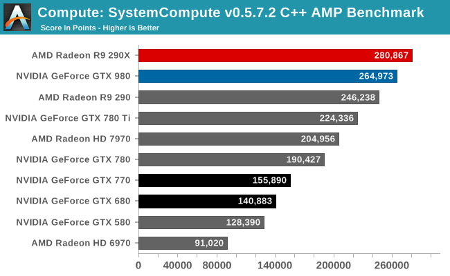
Once again NVIDIA’s compute performance is showing a strong improvement, even under DirectCompute. 17% over GTX 780 Ti and 88% over GTX 680 shows that NVIDIA is getting more work done per CUDA core than ever before. Though this won’t be enough to surpass the even faster R9 290X.
Overall, while NVIDIA can’t win every compute benchmark here, the fact that they are winning so many and by so much – and otherwise not terribly losing the rest – shows that NVIDIA and GM204 have corrected the earlier compute deficiencies in GK104. As an x04 part GM204 may still be first and foremost consumer graphics, but if it’s faced with a compute workload most of the time it’s going to be able to power on through it just as well as it does with games and other graphical workloads.
It would be nice to see GPU compute put to better use than it is today, and having strong(er) compute performance in consumer parts is going to be one of the steps that needs to happen for that outcome to occur.
Power, Temperature, & Noise
As always, last but not least is our look at power, temperature, and noise. Next to price and performance of course, these are some of the most important aspects of a GPU, due in large part to the impact of noise. All things considered, a loud card is undesirable unless there’s a sufficiently good reason – or sufficiently good performance – to ignore the noise.
Having already seen the Maxwell architecture in action with the GTX 750 series, the GTX 980 and its GM204 Maxwell 2 GPU have a very well regarded reputation to live up to. GTX 750 Ti shattered old energy efficiency marks, and we expect much the same of GTX 980. After all, NVIDIA tells us that they can deliver more performance than the GTX 780 Ti for less power than the GTX 680, and that will be no easy feat.
| GeForce GTX 980 Voltages | ||||
| GTX 980 Boost Voltage | GTX 980 Base Voltage | GTX 980 Idle Voltage | ||
| 1.225v | 1.075v | 0.856v | ||
We’ll start as always with voltages, which in this case I think makes for one of the more interesting aspects of GTX 980. Despite the fact that GM204 is a pretty large GPU at 398mm2 and is clocked at over 1.2GHz, NVIDIA is still promoting a TDP of just 165W. One way to curb power consumption is to build a processor wide-and-slow, and these voltage numbers are solid proof that NVIDIA has not done that.
With a load voltage of 1.225v, NVIDIA is driving GM204 as hard (if not harder) than any of the Kepler GPUs. This means that all of NVIDIA’s power optimizations – the key to driving 5.2 billion transistors at under 165W – lie with other architectural optimizations the company has made. Because at over 1.2v, they certainly aren’t deriving any advantages from operating at low voltages.
Next up, let’s take a look at average clockspeeds. As we alluded to earlier, NVIDIA has maintained the familiar 80C default temperature limit for GTX 980 that we saw on all other high-end GPU Boost 2.0 enabled cards. Furthermore as a result of reinvesting most of their efficiency gains into acoustics, what we are going to see is that GTX 980 still throttles. The question then is by how much.
| GeForce GTX 980 Average Clockspeeds | |||
| Max Boost Clock | 1252MHz | ||
| Metro: LL |
1192MHz
|
||
| CoH2 |
1177MHz
|
||
| Bioshock |
1201MHz
|
||
| Battlefield 4 |
1227MHz
|
||
| Crysis 3 |
1227MHz
|
||
| TW: Rome 2 |
1161MHz
|
||
| Thief |
1190MHz
|
||
| GRID 2 |
1151MHz
|
||
| Furmark |
923MHz
|
||
What we find is that while our GTX 980 has an official boost clock of 1216MHz, our sustained benchmarks are often not able to maintain clockspeeds at or above that level. Of our games only Bioshock Infinite, Crysis 3, and Battlefield 4 maintain an average clockspeed over 1200MHz, with everything else falling to between 1151MHz and 1192MHz. This still ends up being above NVIDIA’s base clockspeed of 1126MHz – by nearly 100MHz at times – but it’s clear that unlike our 700 series cards NVIDIA is much more aggressively rating their boost clock. The GTX 980’s performance is still spectacular even if it doesn’t get to run over 1.2GHz all of the time, but I would argue that the boost clock metric is less useful this time around if it’s going to overestimate clockspeeds rather than underestimate. (ed: always underpromise and overdeliver)
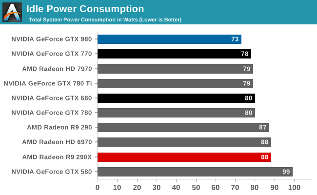
Starting as always with idle power consumption, while NVIDIA is not quoting specific power numbers it’s clear that the company’s energy efficiency efforts have been invested in idle power consumption as well as load power consumption. At 73W idle at the wall, our testbed equipped with the GTX 980 draws several watts less than any other high-end card, including the GK104 based GTX 770 and even AMD’s cards. In desktops this isn’t going to make much of a difference, but in laptops with always-on dGPUs this would be helpful in freeing up battery life.
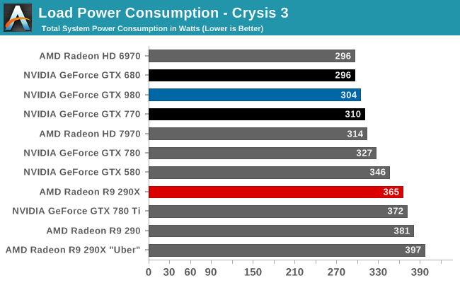
Our first load power test is our gaming test, with Crysis 3. Because we measure from the wall, this test means we’re seeing GPU power consumption as well as CPU power consumption, which means high performance cards will drive up the system power consumption numbers merely by giving the CPU more work to do. This is exactly what happens in the case of the GTX 980; at 304W it’s between the GK104 based GTX 680 and GTX 770, however it’s also delivering 30% better framerates. Accordingly the power consumption of the GTX 980 itself should be lower than either card, but we would not see it in a system power measurement.
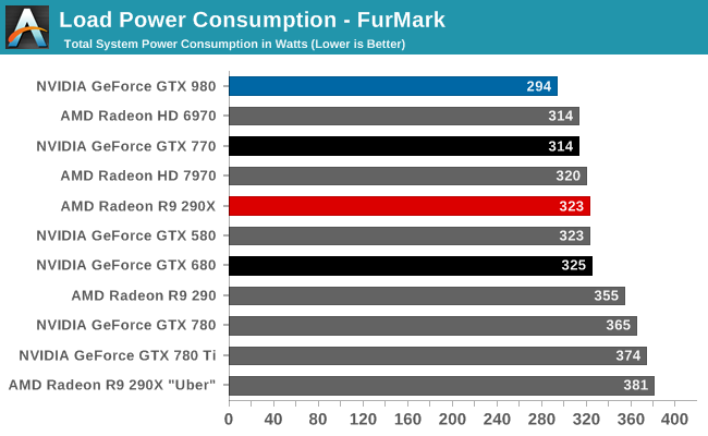
For that reason, when looking at recent generation cards implementing GPU Boost 2.0 or PowerTune 3, we prefer to turn to FurMark as it essentially nullifies the power consumption impact of the CPU. In this case we can clearly see what NVIDIA is promising: GTX 980’s power consumption is lower than everything else on the board, and noticeably so. With 294W at the wall, it’s 20W less than GTX 770, 29W less than 290X, and some 80W less than the previous NVIDIA flagship, GTX 780 Ti. At these power levels NVIDIA is essentially drawing the power of a midrange class card, but with chart-topping performance.
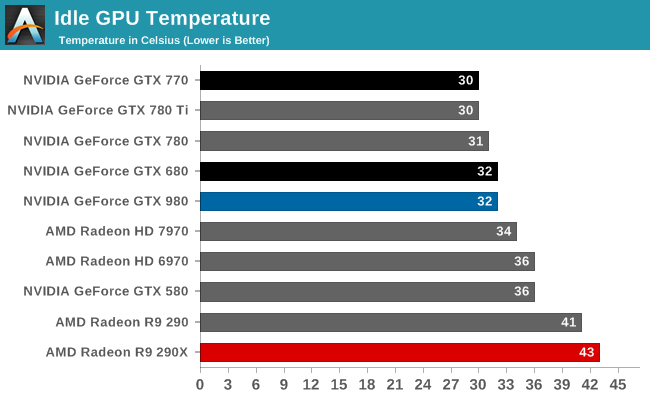
Moving on to temperatures, at idle we see nothing remarkable. All of these well-designed, low idle power designs are going to idle in the low 30s, especially since they’re not more than a few degrees over room temperature.
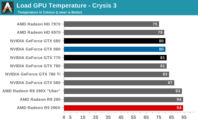
With an 80C throttle point in place for the GTX 980, it’s here where we see the card top out at. The fact that we’re hitting 80C is the reason why the card is exhibiting clockspeed throttling as we saw earlier. NVIDIA’s chosen fan curve is tuned for noise over temperature, so it’s letting the GPU reach its temperature throttle point rather than ramp up the fan (and the noise) too much.
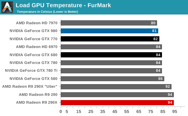
Once again we see the 80C throttle in action. Like all GPU Boost 2.0 NVIDIA cards, NVIDIA makes sure their products aren’t going to get well over 80C no matter the workload.
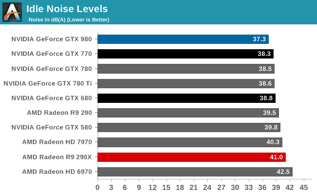
Last but not least we have our noise results. Right off the bat the GTX 980 is looking strong; even with the shared heritage of the cooler with the GTX 780 series, the GTX 980 is slightly but measurably quieter at idle than any other high-end NVIDIA or AMD card. At 37.3dB, the GTX 980 comes very close to being silent compared to the rest of the system.
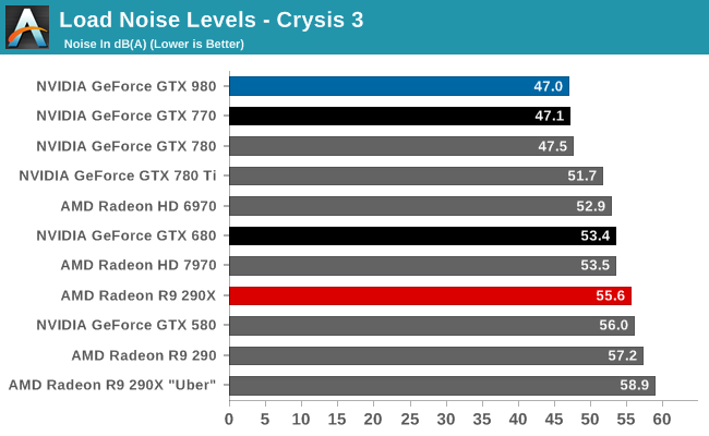
Our Crysis 3 load noise testing showcases the full benefits of the GTX 980’s well-built blower in action. GTX 980 doesn’t perform appreciably better than the GTX Titan cooler equipped GTX 770 and GTX 780, but then again GTX 980 is also not using quite as advanced of a cooler (forgoing the vapor chamber). Still, this is enough to edge ahead of the GTX 770 by 0.1dB, technically making it the quietest video card in this roundup. Though for all practical purposes, it’s better to consider it tied with the GTX 770.
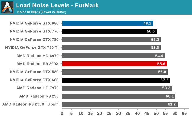
FurMark noise testing on the other hand drives a wedge between the GTX 980 and all other cards, and it’s in the GTX 980’s favor. Despite the similar noise performance between various NVIDIA cards under Crysis 3, under our maximum, pathological workload of FurMark the GTX 980 pulls ahead thanks to its 165W TDP. At the end of the day its lower TDP limit means that the GTX 980 never has too much heat to dissipate, and as a result it never gets too loud. In fact it can’t. 48.1dB is as loud as the GTX 980 can get, which is why the GTX 980’s cooler and overall build are so impressive. There are open air cooled cards that now underperform the GTX 980 that can’t hit these low of noise levels, never mind the other cards with blowers.
Between the GTX Titan and its derivatives and now GTX 980, NVIDIA has spent quite a bit of time and effort on building a better blower, and with their latest effort it really shows. All things considered we prefer blower type coolers for their heat exhaustion benefits – just install it and go, there’s almost no need to worry about what the chassis cooling can do – and with NVIDIA’s efforts to build such a solid cooler for a moderately powered card, the end result is a card with a cooler that offers all the benefits of a blower with the acoustics that can rival and open air cooler. It’s a really good design and one of our favorite aspects of GTX Titan, its derivatives, and now GTX 980.
Overclocking GTX 980
One of GTX 750 Ti’s more remarkable features was its overclocking headroom. GM107 could overclock so well that upon initial release, NVIDIA did not program in enough overclocking headroom in their drivers to allow for many GTX 750 Ti cards to be overclocked to their true limits. This is a legacy we would be glad to see repeated for GTX 980, and is a legacy we are going to put to the test.
As with NVIDIA’s Kepler cards, NVIDIA’s Maxwell cards are subject to NVIDIA’s stringent power and voltage limitations. Overvolting is limited to NVIDIA’s built in overvoltage function, which isn’t so much a voltage control as it is the ability to unlock 1-2 more boost bins and their associated voltages. Meanwhile TDP controls are limited to whatever value NVIDIA believes is safe for that model card, which can vary depending on its GPU and its power delivery design.
For GTX 980 we have a 125% TDP limit, meanwhile we are able to overvolt by 1 boost bin to 1265MHz, which utilizes a voltage of 1.25v.
| GeForce GTX 980 Overclocking | ||||
| Stock | Overclocked | |||
| Core Clock | 1126MHz | 1377MHz | ||
| Boost Clock | 1216MHz | 1466MHz | ||
| Max Boost Clock | 1265MHz | 1515MHz | ||
| Memory Clock | 7GHz | 7.8GHz | ||
| Max Voltage | 1.25v | 1.25v | ||
GTX 980 does not let us down, and like its lower end Maxwell 1 based counterpart the GTX 980 turns in an overclocking performance just short of absurd. Even without real voltage controls we were able to push another 250MHz (22%) out of our GM204 GPU, resulting in an overclocked base clock of 1377MHz and more amazingly an overclocked maximum boost clock of 1515MHz. That makes this the first NVIDIA card we have tested to surpass both 1.4GHz and 1.5GHz, all in one fell swoop.
This also leaves us wondering just how much farther GM204 could overclock if we were able to truly overvolt it. At 1.25v I’m not sure too much more voltage is good for the GPU in the long term – that’s already quite a bit of voltage for a TSMC 28nm process – but I suspect there is some untapped headroom left in the GPU at higher voltages.
Memory overclocking on the other hand doesn’t end up being quite as extreme, but we’ve known from the start that at 7GHz for the stock memory clock, we were already pushing the limits for GDDR5 and NVIDIA’s memory controllers. Still, we were able to work another 800MHz (11%) out of the memory subsystem, for a final memory clock of 7.8GHz.
Before we go to our full results, in light of GTX 980’s relatively narrow memory bus and NVIDIA’s color compression improvements, we quickly broke apart our core and memory overclock testing in order to test each separately. This is to see which overclock has more effect: the core overclock or the memory overclock. One would presume that the memory overclock is the more important given the narrow memory bus, but as it turns out that is not necessarily the case.
| GeForce GTX 980 Overclocking Performance | |||||
| Core (+22%) | Memroy (+11%) | Combined | |||
| Metro: LL |
+15%
|
+4%
|
+20%
|
||
| CoH2 |
+19%
|
+5%
|
+20%
|
||
| Bioshock |
+9%
|
+4%
|
+15%
|
||
| Battlefield 4 |
+10%
|
+6%
|
+17%
|
||
| Crysis 3 |
+12%
|
+5%
|
+15%
|
||
| TW: Rome 2 |
+16%
|
+7%
|
+20%
|
||
| Thief |
+12%
|
+6%
|
+16%
|
||
While the core overclock is greater overall to begin with, what we’re also seeing is that the performance gains relative to the size of the overclock consistently favor the core overclock to the memory overclock. With a handful of exceptions our 11% memory overclock is netting us less than a 6% increase in performance. Meanwhile our 22% core overclock is netting us a 12% increase or more. This despite the fact that when it comes to core overclocking, the GTX 980 is TDP limited; in many of these games it could clock higher if the TDP budget was large enough to accommodate higher sustained clockspeeds.
Memory overclocking is still effective, and it’s clear that GTX 980 spends some of its time memory bandwidth bottlenecked (otherwise we wouldn’t be seeing even these performance gains), but it’s simply not as effective as core overclocking. And since we have more core headroom than memory headroom in the first place, it’s a double win for core overclocking.
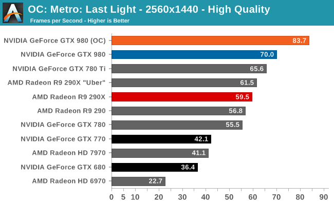
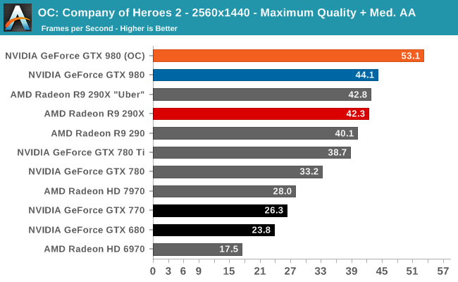
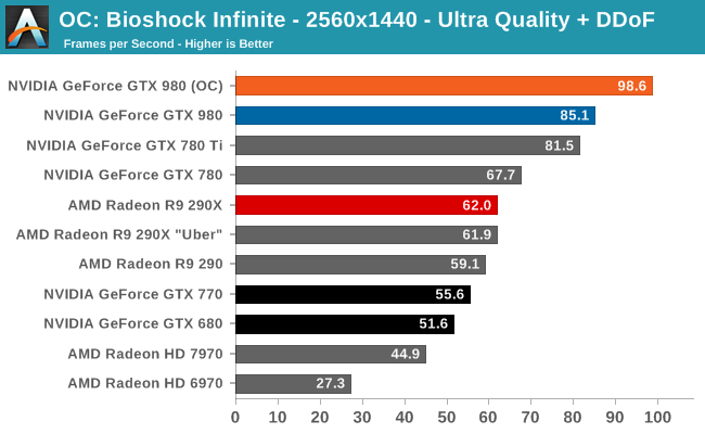
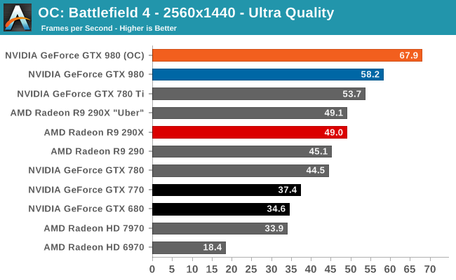
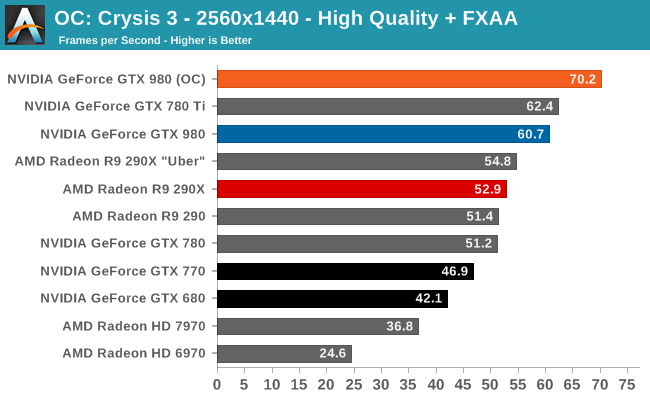
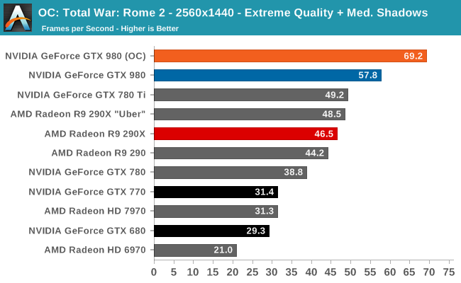
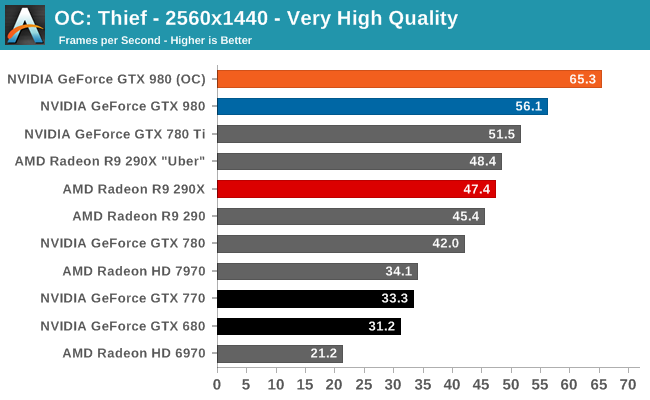
To put it simply, the GTX 980 was already topping the charts. Now with overclocking it’s another 15-20% faster yet. With this overclock factored in the GTX 980 is routinely 2x faster than the GTX 680, if not slightly more.
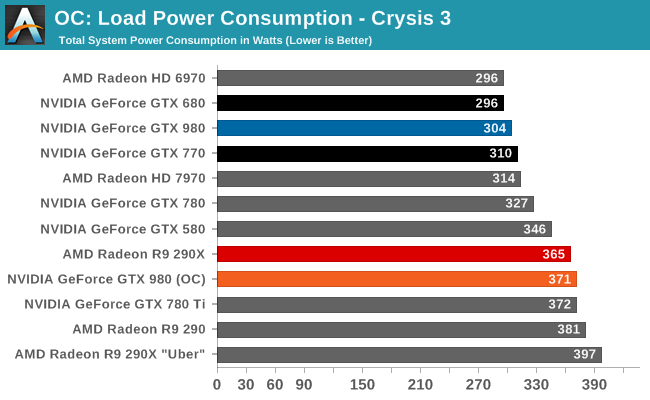
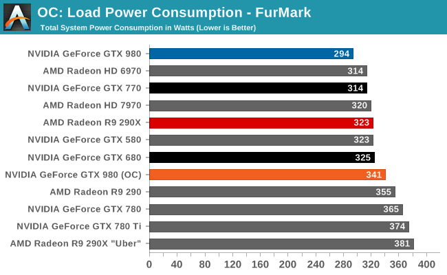
But you do pay for the overclock when it comes to power consumption. NVIDIA allows you to increase the TDP by 25%, and to hit these performance numbers you are going to need every bit of that. So what was once a 165W card is now a 205W card.
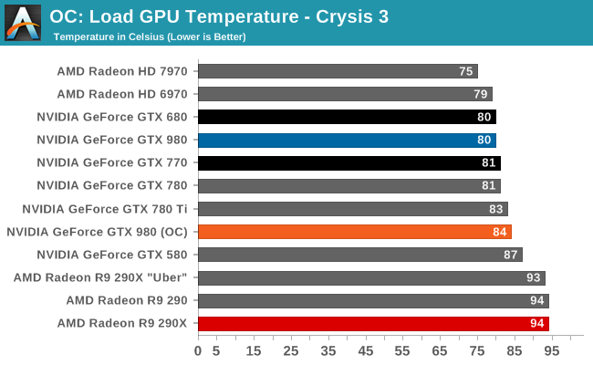
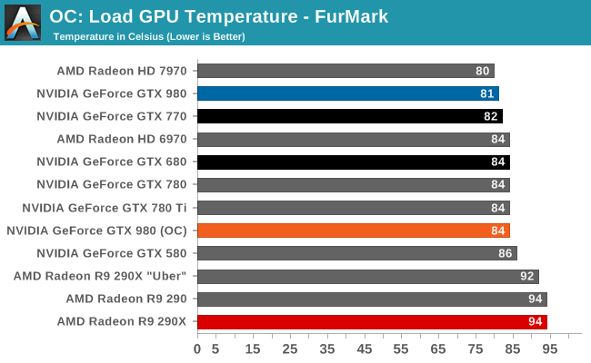
Even though overclocking involves raising the temperature limit to 91C, NVIDIA's fan curve naturally tops out at 84C. So even in the case of overclocking the GTX 980 isn't going to reach temperatures higher than the mid-80s.
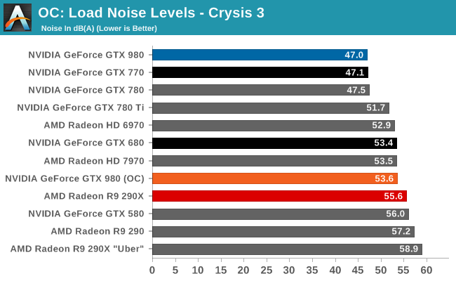
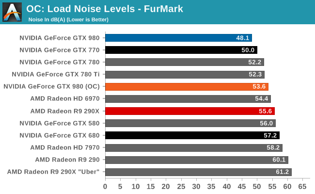
The noise penalty for overclocking is also pretty stiff. Since we're otherwise TDP limited, all of our workloads top out at 53.6dB, some 6.6dB higher than stock. In the big picture this means the overclocked GTX 980 is still in the middl of the pack, but it is noticably louder than before and louder than a few of NVIDIA's other cards. However interestingly enough it's no worse than the original stock GTX 680 at Crysis 3, and still better than said GTX 680 under FurMark. It's also still quieter than the stock Radeon R9 290X, not to mention the louder yet uber mode.
Final Words
When NVIDIA launched the first Maxwell cards earlier this year, we knew that we would be in for a treat with their latest architecture. Though just a fragment of the performance of what their eventual high-end cards would be, NVIDIA’s first Maxwell cards offered an interesting look at an architecture that would be capable of doubling NVIDIA’s performance per watt on the same 28nm TSMC manufacturing process they started with over 2 years ago. To that end I don’t think there has been any doubt that NVIDIA’s eventual second generation Maxwell cards would be equally amazing when it comes to power efficiency, but I feel NVIDIA has still impressed us when it comes to performance, features, and pricing.
In many ways it feels like this latest launch has returned us to the PC video card industry of 2012. NVIDIA’s flagship consumer card is once again powered by a smaller and more potent consumer-class x04 GPU, and once again NVIDIA is swinging the one-two punch of performance and power efficiency. When GTX 680 was launched it set a new high mark for the video card industry, and now we see GTX 980 do more of the same. The GTX 980 is faster, less power hungry, and quieter than the Radeon R9 290X, so once again NVIDIA has landed the technical trifecta. Even if we’re just looking at performance and pricing the GTX 980 is the undisputed holder of the single-GPU performance crown, besting everything else AMD and NVIDIA have to offer, and offering it at a price that while no means a steal is more than reasonable given NVIDIA’s technical and performance advantage. As such GTX 980 comes very, very close to doing to Radeon R9 290X what GTX 680 did to Radeon HD 7970 over 2 years ago.
Meanwhile from a feature perspective the GTX 900 series is going to prove to be a very captivating product. Dynamic Super Resolution is a brutish-yet-clever solution of what to do about anti-aliasing on today's deferred renderer games that cannot support traditional MSAA/SSAA, and while I’m withholding my judgment on Multi-Frame sampled Anti-Aliasing until it’s made available to users in NVIDIA’s drivers, the idea at least has merit. Otherwise I am very happy to see that NVIDIA has now fully caught up to the competition in terms of baseline API features by offering everything needed to support Direct3D 11.2 and beyond.
Along those lines, NVIDIA’s focus on voxel technology for Maxwell 2 is a very interesting route to take, and I am eagerly anticipating seeing whether it gets widely adopted and what developers do with it. VXGI is a very neat concept to generate voxel based global illumination, and building in the features necessary to do significant portions of it in hardware is a wise move by NVIDIA. The catch at this point is the same catch that faces all vendor specific technologies: just because the hardware is there doesn’t mean developers will put it to good use, especially in this age of console ports. NVIDIA for their part has made the right move by making sure VXGI will run on other hardware, but I am concerned that the performance delta means that it’s only going to be viable on Maxwell 2 GPUs for now, which could discourage developers. None the less we do need better lighting in games, and I hope this encourages developers to finally adopt these kinds of high quality global illumination systems.
As for the hardware itself, is there anything left to say other than that GTX 980 is a well-built, well-engineered card? The build quality is impeccable – raising the bar over even GTX Titan – and the power efficiency gains are truly remarkable. With a TDP lower than even GTX 680, this is the lowest power consumption has been for a chart-topping card since 9800 GTX over half a decade ago. It’s really a bit of a honeymoon period since if and when NVIDIA does Big Maxwell one has to expect power consumption will go back up, but for the time being it’s very pleasing to be able to get chart-topping performance inside of 165W. And the fact that this comes from the same company responsible for GTX 480 just 2 generations ago makes this the ultimate technical turnaround.
In conclusion, the GeForce GTX 980 represents another stellar performance from NVIDIA. Their reign at the top is not going to go unchallenged – AMD can’t match NVIDIA on performance, but they can sure drive down prices – but as was the case in 2012 the crown continues to securely reside in NVIDIA’s hands, and once again they have done the technical hard work to earn it.
Finally, as a reminder we will be following up this article next week with our look at GTX 980 SLI performance and a look at the GTX 970. Of the two cards launched today the GTX 970 is without a doubt the more interesting of the two thanks to its relatively low price compared to the performance NVIDIA is offering, but due to our aforementioned board issues we will not be able to take a look at it until next week. So until then stay tuned for the rest of our GM204 coverage.

