Original Link: https://www.anandtech.com/show/8460/amd-radeon-r9-285-review
AMD Radeon R9 285 Review: Feat. Sapphire R9 285 Dual-X OC
by Ryan Smith on September 10, 2014 2:00 PM EST
Last month AMD held their 30 years of graphics celebration, during which they announced their next Radeon video card, the Radeon R9 285. Designed to be AMD’s new $249 midrange enthusiast card, the R9 285 would be launching on September 2nd. In the process the R9 285 would be a partial refresh of their R9 280 series lineup, supplying it with a new part that would serve to replace their nearly 3 year old Tahiti GPU.
The R9 285 is something of a lateral move for AMD, which is something we very rarely see in this industry. The R9 285’s immediate predecessor, the R9 280 (vanilla) has been on the market with an MSRP of $249 for nearly 4 months now. Meanwhile the R9 285 is not designed to be meaningfully faster than the R9 280 – in fact if you looked at the raw specifications, you’d rightfully guess it would be slower. Instead the R9 285 is intended to serve as a sort of second-generation feature update to R9 280, replacing it with a card at the same price with roughly the same performance level, but with 3 years’ worth of amassed feature updates and optimizations.
To accomplish this AMD has minted a new GPU, Tonga. We’ll go into more detail on Tonga in a bit, but at its core Tonga is in many ways an optimized version of Tahiti. More importantly though, Tonga is also the first GPU in AMD’s next Graphics Core Next architecture revision, which we will come to know as GCN 1.2. As a result, this launch won’t come with a significant shift in AMD’s performance-value, but for buyers it offers an improved feature set for those apprehensive about buying into Tahiti 3 years later, and for enthusiast it offers us a look at what the next iteration of AMD’s GPUs will look like.
| AMD GPU Specification Comparison | ||||||
| AMD Radeon R9 290 | AMD Radeon R9 280X | AMD Radeon R9 285 | AMD Radeon R9 280 | |||
| Stream Processors | 2560 | 2048 | 1792 | 1792 | ||
| Texture Units | 160 | 128 | 112 | 112 | ||
| ROPs | 64 | 32 | 32 | 32 | ||
| Core Clock | 662MHz | 850MHz | ? | 827MHz | ||
| Boost Clock | 947MHz | 1000MHz | 918MHz | 933MHz | ||
| Memory Clock | 5GHz GDDR5 | 6GHz GDDR5 | 5.5GHz GDDR5 | 5GHz GDDR5 | ||
| Memory Bus Width | 512-bit | 384-bit | 256-bit | 384-bit | ||
| VRAM | 4GB | 3GB | 2GB | 3GB | ||
| FP64 | 1/8 | 1/4 | 1/16 | 1/4 | ||
| TrueAudio | Y | N | Y | N | ||
| Typical Board Power | 250W | 250W | 190W | 250W | ||
| Manufacturing Process | TSMC 28nm | TSMC 28nm | TSMC 28nm | TSMC 28nm | ||
| Architecture | GCN 1.1 | GCN 1.0 | GCN 1.2 | GCN 1.0 | ||
| GPU | Hawaii | Tahiti | Tonga | Tahiti | ||
| Launch Date | 11/05/13 | 10/11/13 | 09/02/14 | 03/04/14 | ||
| Launch Price | $399 | $299 | $249 | $279 | ||
Diving into the R9 285’s raw specifications, the card utilizes a 1792 stream processor Graphics Core Next GPU. Paired with these SPs are 112 texture units (in the standard 16:1 ratio), and on the backend of the rendering pipeline is 32 ROPs. As is unfortunately consistent for AMD, they are not disclosing the product’s base clockspeed, but they have published the boost clockspeed of 918MHz.
Meanwhile feeding R9 285’s GPU falls to the card’s 2GB of GDDR5. This is on a 256-bit bus, and is clocked at 5.5GHz for a total memory bandwidth of 176GB/sec.
The R9 285 will have a rated typical board power (AMD’s analogue for TDP) of 190W. Notably this is only 10W higher than the Pitcairn based R9 270X despite the 40% larger SP count, or alternatively is 60W lower than the Tahiti based R9 280. Taking into consideration the R9 270X comparison in particular, it’s clear that AMD has done some work on efficiency to squeeze out more compared to the GCN 1.0 based Pitcairn and Tahiti parts that R9 285 is going to be competing with.
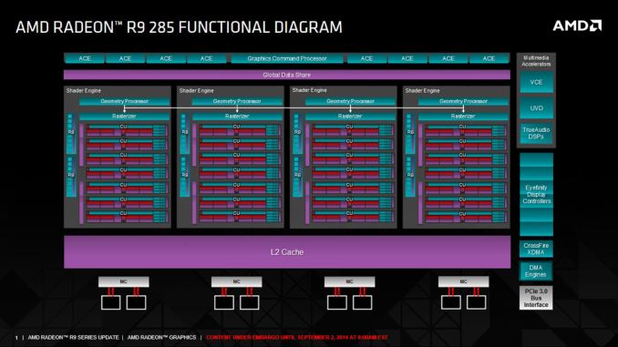
The GPU itself, Tonga, is AMD’s first released GCN 1.2 GPU, with R9 285 arriving before the previously announced Tonga-based FirePro W7100. We’ll dive into further detail into GCN 1.2 on the following pages, but from a high level overview Tonga looks a lot like an optimized Tahiti. AMD has confirmed that R9 285 is not utilizing a “full” Tonga configuration, so R9 285 is not the highest possible configuration for Tonga.
A complete Tonga configuration will contain 2048 SPs, just like its Tahiti predecessor, with 1792 of those SPs active on R9 285. This is paired with the card’s 32 ROPs attached to a 256-bit memory bus, and a 4-wide (4 geometry processor) frontend. Compared to Tahiti the most visible change is the memory bus size, which has gone from 384-bit to 256-bit. In our look at GCN 1.2 we’ll see why AMD is able to get away with this – the short answer is compression – but it’s notable since at an architectural level Tahiti had to use a memory crossbar between the ROPs and memory bus due to their mismatched size (each block of 4 ROPs wants to be paired with a 32bit memory channel). The crossbar on Tahiti exposes the cards to more memory bandwidth, but it also introduces some inefficiencies of its own that make the subject a tradeoff.
Meanwhile Tonga’s geometry frontend has received an upgrade similar to Hawaii’s, expanding the number of geometry units (and number of polygons per clock) from 2 to 4. And there are actually some additional architectural efficiency improvements in here that should further push performance per clock beyond what Hawaii can do in the real world.
The final die size of Tonga is 359mm2 and it packs an unexpectedly high 5 billion transistors. Compared to Tahiti, this is a very slight (7mm2) increase in die size, while the transistor count has gone up by nearly 700M from Tahiti’s 4.31B transistors. Tonga’s configuration and die size indicate that AMD has made some interesting tradeoffs in terms of die size and features. The narrower memory bus means that AMD was able to drop a pair of memory controllers and the memory crossbar, only for AMD to fill it in with the additional transistors needed to drive all of the additional features (and geometry processors) that Tahiti lacked.
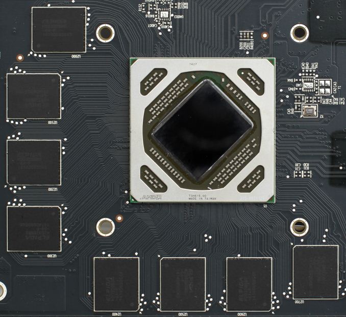
Tonga & VRAM. Image Courtesy Hardware.FR
Consequently R9 285 isn’t just a lateral in performance, but from a die size and cost standpoint it should be equally lateral, with Tonga being roughly as expensive to produce as Tahiti. However final boards should be slightly cheaper to produce than R9 280 boards – the 256-bit memory bus allows for simpler boards, it only has 2GB of VRAM instead of 3GB, and the reduced power consumption allows for less complex power delivery circuitry.
Otherwise when it comes to features, being GCN 1.2 based means that the R9 285 will bring with it support for all of the features first introduced in GCN 1.1. This includes support for True Audio, support for bridgeless CrossFire thanks to the XDMA engine, GCN 1.1’s superior boost mechanism, and full support for AMD’s upcoming FreeSync implementation of DisplayPort Adaptive Sync (GCN 1.0 GPUs are not fully adaptive).
AMD will be positioning the R9 285 to compete with NVIDIA’s GeForce GTX 760, the company’s second-tier GK104 part. The R9 280 already compares favorably to the GTX 760, so AMD needs only to not regress to maintain their competitiveness. Meanwhile the GTX 760 was until recently frequently found at $239 – a hair under the R9 285’s launch price – and has since fallen to around $219 in response to the R9 285. What this means is that the GTX 760 has slowly withdrawn itself from competition, taking up a position as a lower performance but cheaper card. It's still NVIDIA's closest competitor at this time, but NVIDIA has wisely realized that they can find a more comfortable spot below the R9 285 rather than trying to compete head-on with it.
The launch of the R9 285 has been a hard launch, and with AMD’s partners producing their own designs this is a pure virtual launch (no reference card) with an MSRP of $249. In our briefing AMD also told us that there will be both 2GB and 4GB cards, and from past experience with split launches like these, we’re expecting most cards to be of the 2GB variety. In fact of the first wave of cards that have hit the market, all of them are 2GB cards with 4GB cards yet to reach shelves. Partially due to this lag between 2GB and 4GB parts, AMD hasn’t been able to give us an estimate on what the 4GB price premium is, but it’s going to be an important fact to take into consideration as the suitability of 2GB enthusiast cards has been challenged by the presence of so much RAM on the current-generation consoles, which will have a knock-on effect on console-to-PC ports.
Meanwhile with the launch of the R9 285 and impending discontinuation of the R9 280, buyers looking at picking up an R9 285 in the near term will have to be on the lookout for R9 280 on clearance sale. It’s already regularly found for $220 and lower, making it $30+ cheaper than the R9 285 and possessing 3GB of VRAM to the R9 285’s 2GB. This will make the R9 280 a strong contender, at least until supplies run out.
Finally, coinciding with the launch of the R9 285 will be a refresh of AMD’s Never Settle bundles. At the gold tier, which will encompass the entire R9 series, AMD is adding Alien: Isolation, and atypically a feature-limited (non-full) copy of Star Citizen to the lineup.
| Fall 2014 GPU Pricing Comparison | |||||
| AMD | Price | NVIDIA | |||
| Radeon R9 290 | $400 | ||||
| $310 | GeForce GTX 770 | ||||
| Radeon R9 280X | $280 | ||||
| Radeon R9 285 | $250 | ||||
| Radeon R9 280 | $220 | GeForce GTX 760 | |||
| Radeon R9 270X | $180 | ||||
| $160 | GeForce GTX 660 | ||||
Tonga’s Microarchitecture - What We’re Calling GCN 1.2
As we alluded to in our introduction, Tonga brings with it the next revision of AMD’s GCN architecture. This is the second such revision to the architecture, the last revision (GCN 1.1) being rolled out in March of 2013 with the launch of the Bonaire based Radeon HD 7790. In the case of Bonaire AMD chose to kept the details of GCN 1.1 close to them, only finally going in-depth for the launch of the high-end Hawaii GPU later in the year. The launch of GCN 1.2 on the other hand is going to see AMD meeting enthusiasts half-way: we aren’t getting Hawaii level details on the architectural changes, but we are getting an itemized list of the new features (or at least features AMD is willing to talk about) along with a short description of what each feature does. Consequently Tonga may be a lateral product from a performance standpoint, but it is going to be very important to AMD’s future.
But before we begin, we do want to quickly remind everyone that the GCN 1.2 name, like GCN 1.1 before it, is unofficial. AMD does not publicly name these microarchitectures outside of development, preferring to instead treat the entire Radeon 200 series as relatively homogenous and calling out feature differences where it makes sense. In lieu of an official name and based on the iterative nature of these enhancements, we’re going to use GCN 1.2 to summarize the feature set.
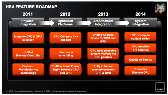
AMD's 2012 APU Feature Roadmap. AKA: A Brief Guide To GCN
To kick things off we’ll pull old this old chestnut one last time: AMD’s HSA feature roadmap from their 2012 financial analysts’ day. Given HSA’s tight dependence on GPUs, this roadmap has offered a useful high level overview of some of the features each successive generation of AMD GPU architectures will bring with it, and with the launch of the GCN 1.2 architecture we have finally reached what we believe is the last step in AMD’s roadmap: System Integration.
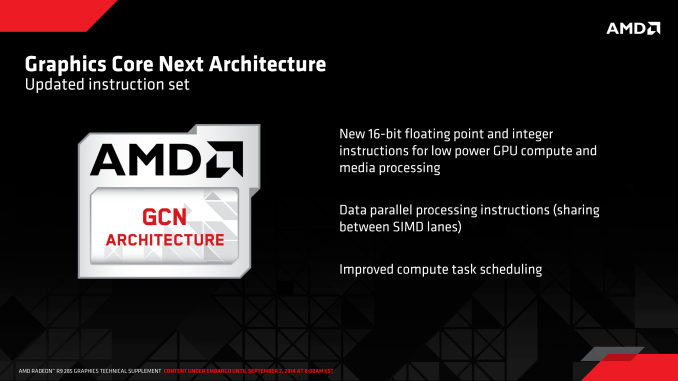
It’s no surprise then that one of the first things we find on AMD’s list of features for the GCN 1.2 instruction set is “improved compute task scheduling”. One of AMD’s major goals for their post-Kavari APU was to improve the performance of HSA by various forms of overhead reduction, including faster context switching (something GPUs have always been poor at) and even GPU pre-emption. All of this would fit under the umbrella of “improved compute task scheduling” in AMD’s roadmap, though to be clear with AMD meeting us half-way on the architecture side means that they aren’t getting this detailed this soon.
Meanwhile GCN 1.2’s other instruction set improvements are quite interesting. The description of 16-bit FP and Integer operations is actually very descriptive, and includes a very important keyword: low power. Briefly, PC GPUs have been centered around 32-bit mathematical operations for some number of years now since desktop technology and transistor density eliminated the need for 16-bit/24-bit partial precision operations. All things considered, 32-bit operations are preferred from a quality standpoint as they are accurate enough for many compute tasks and virtually all graphics tasks, which is why PC GPUs were limited to (or at least optimized for) partial precision operations for only a relatively short period of time.
However 16-bit operations are still alive and well on the SoC (mobile) side. SoC GPUs are in many ways a 5-10 year old echo of PC GPUs in features and performance, while in other ways they’re outright unique. In the case of SoC GPUs there are extreme sensitivities to power consumption in a way that PCs have never been so sensitive, so while SoC GPUs can use 32-bit operations, they will in some circumstances favor 16-bit operations for power efficiency purposes. Despite the accuracy limitations of a lower precision, if a developer knows they don’t need the greater accuracy then falling back to 16-bit means saving power and depending on the architecture also improving performance if multiple 16-bit operations can be scheduled alongside each other.
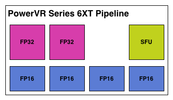
Imagination's PowerVR Series 6XT: An Example of An SoC GPU With FP16 Hardware
To that end, the fact that AMD is taking the time to focus on 16-bit operations within the GCN instruction set is an interesting one, but not an unexpected one. If AMD were to develop SoC-class processors and wanted to use their own GPUs, then natively supporting 16-bit operations would be a logical addition to the instruction set for such a product. The power savings would be helpful for getting GCN into the even smaller form factor, and with so many other GPUs supporting special 16-bit execution modes it would help to make GCN competitive with those other products.
Finally, data parallel instructions are the feature we have the least knowledge about. SIMDs can already be described as data parallel – it’s 1 instruction operating on multiple data elements in parallel – but obviously AMD intends to go past that. Our best guess would be that AMD has a manner and need to have 2 SIMD lanes operate on the same piece of data. Though why they would want to do this and what the benefits may be are not clear at this time.
GCN 1.2: Geometry Performance & Color Compression
Instruction sets aside, Radeon R9 285 is first and foremost a graphics and gaming product, so let’s talk about what GCN 1.2 brings to the table for those use cases.
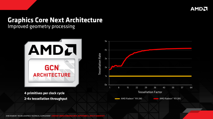
Through successive generations of GPU architectures AMD has been iterating on and improving their geometry hardware, both at the base level and in the case of geometry generated through tessellation. This has alternated between widening the geometry frontends and optimizing the underlying hardware, with the most recent update coming in the GCN 1.1 based Hawaii, which increased AMD’s geometry processor count at the high end to 4 processors and implemented some buffering enhancements.
For Tonga AMD is bringing that 4-wide geometry frontend from Hawaii, which like Hawaii immediately doubles upon Tahiti’s 2-wide geometry frontend. Not stopping there however, AMD is also implementing a new round of optimizations to further improve performance. GCN 1.2’s geometry frontend includes improved vertex reuse (for better performance with small triangles) and improved work distribution between the geometry frontends to better allocate workloads between them.
At the highest level Hawaii and Tonga should be tied for geometry throughput at equivalent clockspeeds, or roughly 2x faster than Tahiti. However in practice due to these optimizations Tonga’s geometry frontend is actually faster than Hawaii’s in at least some cases, as our testing has discovered.
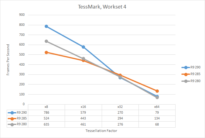
Comparing the R9 290 (Hawaii), R9 285 (Tonga), and R9 280 (Tahiti) in TessMark at various tessellation factors, we have found that while Tonga trails Hawaii at low tessellation factors – and oddly enough even Tahiti – at high tessellation factors the tables are turned. With x32 and x64 tessellation, the Tonga based R9 285 outperforms both cards in this raw tessellation test, and at x64 in particular completely blows away Hawaii, coming close to doubling its tessellation performance.
At the x64 tessellation factor we see the R9 285 spit out 134fps, or equivalent to roughly 1.47B polygons/second. This is as compared to 79fps (869M Polys/sec) for the R9 290, and 68fps (748M Polys/sec) for the R9 280. One of the things we noted when initially reviewing the R9 290 series was that AMD’s tessellation performance didn’t pick up much in our standard tessellation benchmark (Tessmark at x64) despite the doubling of geometry processors, and it looks like AMD has finally resolved that with GCN 1.2’s efficiency improvements. As this is a test with a ton of small triangles, it looks like we’ve hit a great case for the vertex reuse optimizations.
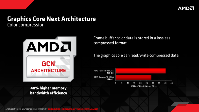
Meanwhile AMD’s other GCN 1.2 graphics-centric optimization comes at the opposite end of the rendering pipeline, where the ROPs and memory controllers lie. As we mentioned towards the start of this article, one of the notable changes between the R9 280 and R9 285 is that the latter utilizes a smaller 256-bit memory bus versus the R9 280’s larger 384-bit memory bus, and as a result has around 27% less memory bandwidth than the R9 280. Under most circumstances such a substantial loss in memory bandwidth would result in a significant performance hit, so for AMD to succeed Tahiti with a smaller memory bus, they needed a way to be able to offset that performance loss.
The end result is that GCN 1.2 introduces a new color compression method for its ROPs, to reduce the amount of memory bandwidth required for frame buffer operations. Color compression itself is relatively old – AMD has had color compression in some form for almost 10 years now – however GCN 1.2 iterates on this idea with a color compression method AMD is calling “lossless delta color compression.”
Since AMD is only meeting us half-way here we don’t know much more about what this does. Though the fact that they’re calling it delta compression implies that AMD has implemented a further layer of compression that works off of the changes (deltas) in frame buffers, on top of the discrete compression of the framebuffer. In this case this would not be unlike modern video compression codecs, which between keyframes will encode just the differences to reduce bandwidth requirements (though in AMD’s case in a lossless manner).
AMD’s own metrics call for a 40% gain in memory bandwidth efficiency, and if that is the average case it would more than make up for the loss of memory bandwidth from working on a narrower memory bus. We’ll see how this plays out over our individual games over the coming pages, but it’s worth noting that even our most memory bandwidth-sensitive games hold up well compared to the R9 280, never losing anywhere near the amount of performance that such a memory bandwidth reduction would imply (if they lose performance at all).
GCN 1.2 - Image & Video Processing
AMD’s final set of architectural improvements for GCN 1.2 are focused on image and video processing blocks contained within the GPU. These blocks, though not directly tied to GPU performance, are important to AMD by enabling new functionality and by offering new ways to offload tasks on to fixed function hardware for power saving purposes.
First and foremost then, with GCN 1.2 comes a new version of AMD’s video decode block, the Unified Video Decoder. It has now been some time since UVD has received a significant upgrade, as outside of the addition of VC-1/WMV9 support it has remained relatively unchanged for a couple of GPU generations.
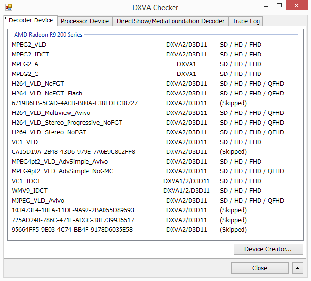
With this newest generation of UVD, AMD is finally catching up to NVIDIA and Intel in H.264 decode capabilities. New to UVD is full support for 4K H.264 video, up to level 5.2 (4Kp60). AMD had previously intended to support 4K up to level 5.1 (4Kp30) on the previous version of UVD, but that never panned out and AMD ultimately disabled that feature. So as of GCN 1.2 hardware decoding of 4K is finally up and working, meaning AMD GPU equipped systems will no longer have to fall back to relatively expensive software decoding for 4K H.264 video.
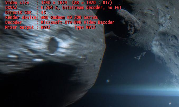
On a performance basis this newest iteration of UVD is around 3x faster than the previous version. Using DXVA checker we benchmarked it as playing back a 1080p video at 331fps, or roughly 27x real-time. For 1080p decode it has enough processing power to decode multiple streams and then-some, but this kind of performance is necessary for the much higher requirements of 4K decoding.
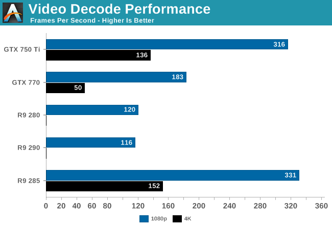
Speaking of which, we can confirm that 4K decoding is working like a charm. While Media Player Classic Home Cinema’s built-in decoder doesn’t know what to do for 4K on the new UVD, Windows’ built-in codec has no such trouble. Playing back a 4K video using that decoder hit 152fps, more than enough to play back a 4Kp60 video or two. For the moment this also gives AMD a leg-up over NVIDIA; while Kepler products can handle 4Kp30, their video decoders are too slow to sustain 4Kp60, which is something only Maxwell cards such as 750 Ti can currently do. So at least for the moment with R9 285’s competition being composed of Kepler cards, it’s the only enthusiast tier card capable of sustaining 4Kp60 decoding.
This new version of UVD also expands AMD’s supported codec set by 1 with the addition of hardware MJPEG decoding. AMD has previously implemented JPEG decoding for their APUs, so MJPEG is a natural extension of that. Though MJPEG is a fairly uncommon codec for most workloads these days, so outside of perhaps pro video I’m not sure how often this feature will get utilized.
What you won’t find though – and we’re surprised it’s not here – is support for H.265 decoding in any form. While we’re a bit too early for full fixed function H.265 decoders since the specification was only ratified relatively recently, both Intel and NVIDIA have opted to bridge the gap by implementing a hybrid decode mode that mixes software, GPU shader, and fixed function decoding steps. H.265 is still in its infancy, but given the increasingly long shelf lives of video cards, it’s a reasonable bet that Tonga cards will still be in significant use after H.265 takes off. But to give AMD some benefit of the doubt, since a hybrid mode is partially software anyhow, there’s admittedly nothing stopping them from implementing it in a future driver (NVIDIA having done just this for H.265 on Kepler).
Moving on, along with their video decode capabilities, AMD has also improved on their video encode capabilities for GCN 1.2 with a new version of their Video Codec Engine. AMD’s hardware video encoder has received a speed boost to improve its encoding performance at all levels, and after previously being limited to a maximum resolution of 1080p can now encode at resolutions up to 4K. Meanwhile by AMD’s metrics this new version of VCE should be capable of encoding 1080p up to 12x over real time.
A quick performance check finds that while the current version of Cyberlink’s MediaEspresso software isn’t handling 4K video decoding quite right, encoding from a 1080p source shows that the new VCE is roughly 40% faster than the old VCE in our test.
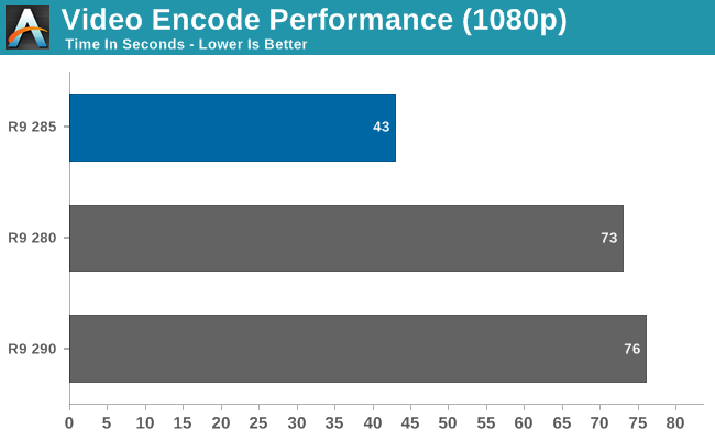
4K video is still rather new, so there’s little to watch and even less of a reason to encode. That of course will change over time, but in the meantime the most promising use of a hardware 4K encoder would be 4K gameplay recording through the AMD Gaming Evolved Client’s DVR function.
Meet The Sapphire R9 285 Dual-X OC 2GB
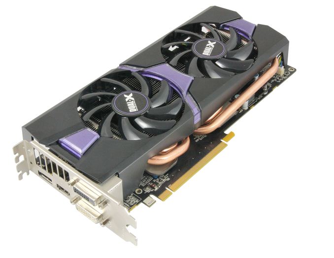
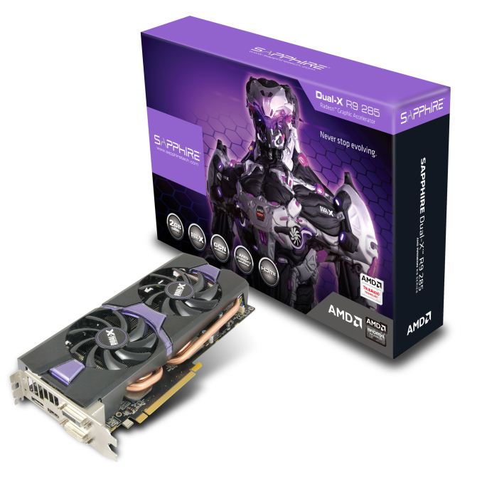
Our sample provided by AMD for today’s launch is Sapphire’s R9 285 Dual-X OC 2GB. As we mentioned before this is a non-reference launch, so rather than ship out engineering cards that won’t see retail AMD has sent us proper retail cards.
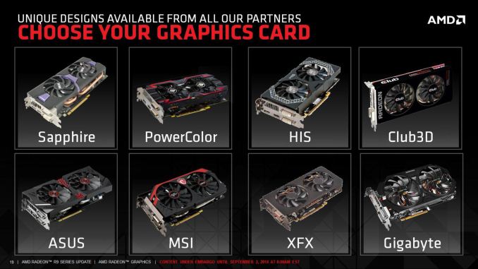
Sapphire’s R9 285 Dual-X OC is in turn a good example of what kinds of cards are appearing on store shelves. As R9 285 is a sub-200W product all of the launch cards have followed the same basic design, utilizing their manufacturer’s respective dual fan open air designs. So if you like full size open air cards then you’ll have your pick of the litter. However it also means that there aren’t any blowers on the market – nor do we expect any in the development pipeline – so for the moment the market for R9 285s is rather homogenous. In Sapphire’s case, though not available at launch, we will eventually see them break the mold with a smaller single-fan card specifically designed for use in ITX systems.
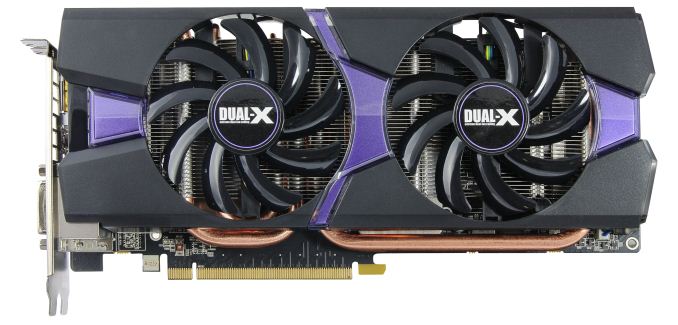
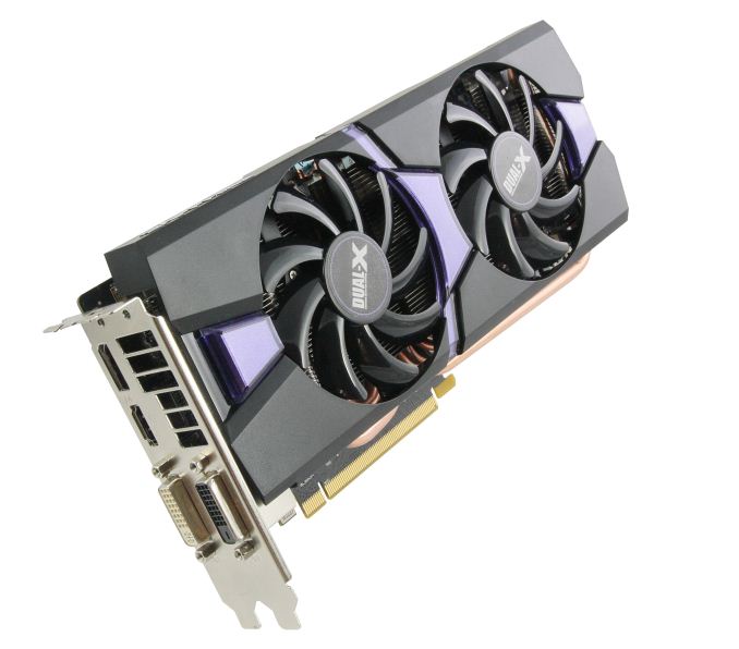
But getting to the R9 285 Dual-X OC, the Dual-X is a solid entry from Sapphire that is very typical of their current designs. As given away by the name, this card utilizes a 10” version of Sapphire’s Dual-X open-air cooler, and among Sapphire’s product lineup it can be considered the company’s baseline cooler for products up to 250W. Meanwhile as an OC model Sapphire is shipping this card with a mild factory overclock of 965MHz for the core and 5.6GHz for the memory, which represents a 47MHz (5%) core overclock and 100MHz (2%) memory overclock. Though note that Sapphire is also producing an identical version of this hardware without the factory overclock.
Continuing with our overall theme of R9 285 being a lateral product for AMD, the same is unsurprisingly true for Sapphire. For the R9 285 Dual-X Sapphire has opted to port over the design of their existing R9 280 Dual-X (which happens to be our R9 280 test card), building a suitable new PCB for Tonga but otherwise retaining the R9 280’s cooler and functionality. With R9 280 being a more power hungry part (on paper at least), this means the R9 285 Dual-X cooler is slightly overpowered in comparison, which should bode well for temperature/acoustic performance and for overclocking.
The Dual-X cooler itself is something of a tried and true design for Sapphire at this point, as years of iteration on dual fan coolers has resulted in these designs coalescing into similar and highly effective coolers. Starting from the top, the 10” version of the Dual-X cooler utilizes a pair of 85mm fans, allowing it to provide more than sufficient airflow for the primary and VRM heatsinks. Buyers with cramped cases will want to note that the use of such a large fan does result in a shroud larger than the PCB itself, with the shroud extending an additional 1cm over the PCB.
Below the fans we find Sapphire’s primary heatsink, which is composed of aluminum and runs just short of the entire length of the cooler. Sapphire attaches the primary heatsink to the GPU through the use of 4 copper heatpipes which run between the GPU and various points on the heatsink. The heatpipes in turn do not make direct contact with the GPU, but instead attach to a copper baseplate which in turn is what makes contact with the GPU and channels heat into the heatpipes.
Surrounding the copper baseplate is a secondary aluminum baseplate which provides both structure for the overall heatsink and additional cooling. Through the use of thermal pads, the aluminum baseplate covers the card’s RAM chips, providing direct cooling for the RAM. Meanwhile the card’s VRMs are not part of the primary heatsink assembly, and are instead cooled via a smaller secondary “strip” heatsink that sits over the MOSFETs towards the rear of the card. Airflow making it through the primary heatsink is in turn responsible for cooling this secondary heatsink.
Removing the heatsink and accessing the PCB, Sapphire’s PCB is typical for a 200W card. Sapphire places the bulk of the VRM circuitry towards the rear of the card, between the GPU/RAM and the PCIe power sockets. Meanwhile Sapphire’s RAM of choice is 6GHz Elpedia, which means this card ships at a lower memory frequency than what the RAM is capable of. For overclockers this means there’s some guaranteed headroom on the RAM, while the lower shipping frequency may indicate that AMD has tuned Tonga’s memory controllers for sub-6GHz operation, similar to what happened with Hawaii.
Throughout all of this the R9 285 Dual-X OC is generally a solid card, but the heatsink/PCB interaction does expose the card’s one real weakness/design flaw, which is a lack of rigidity. As is almost always the case with these large heatsink cards, the heatsink is massive enough that for all practical purposes the PCB is attached to the heatsink rather than vice versa. However Sapphire only attaches the heatsink to the PCB at the 4 screws around the GPU, which for a 10.25” card means the far end of the card is far removed from these attachment points and is left free to flex. Sapphire does include a plastic leg at one corner of the shroud to keep the PCB from flexing too much, but this leg isn’t secured to the PCB and indeed isn’t even long enough to touch the PCB without flexing. Ideally we would like to see all 9”+ cards reinforced against flexing for this reason, either by securing the shroud to the PCB at the rear of the card or by employing a stiffener along the top edge of the PCB.
Moving on, Sapphire doesn’t list an official TDP for the R9 285 Dual-X OC, however given the factory overclock it’s fair to say that in practice it’s going to be a bit higher than AMD’s official 190W TDP of a stock R9 285. Providing power for the card is a pair of 6pin PCIe power connectors at the top-rear of the card, which along with the PCIe slot connector means the card has the means to deliver up to 225W of power (VRMs willing). Interestingly Sapphire’s PCB has an additional pair of solder points for replacing one of the 6pin connectors with an 8pin connector, which may indicate a future Sapphire card or Sapphire hedging their bets for the inevitable higher tier Tonga card with all 32 CUs enabled.
Meanwhile though you won’t find a Crossfire connector at the top of the card – having been made obsolete by GCN 1.1+’s XDMA engines – what you will find on the Sapphire card is a BIOS switch. Sapphire ships the R9 285 Dual-X as a dual BIOS UEFI card, with one BIOS for legacy systems and a second BIOS for UEFI systems. The card’s default shipping state will be for the legacy BIOS, while depressing the BIOS button will switch to UEFI. Outside of reference cards we don’t see too many dual BIOS cards, and given the limited selection of such cards we are rather fond of the fact that Sapphire uses a button here as opposed to a more difficult to access switch.
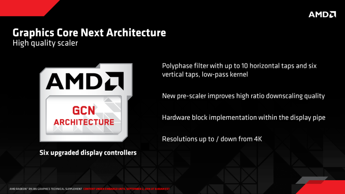
Finally, towards the front of the card we see the standard AMD 200 series I/O configuration of 1x DL-DVI-I, 1x DL-DVI-D, 1x HDMI, and 1x DisplayPort. Tonga has up to 6 display controllers, and while not easy it should be possible to use all 6 of them through a careful use of MST off of the DisplayPort and identical monitors hanging off of the HDMI and DVI ports.
Wrapping things up, the retail price on the R9 285 Dual-X OC is currently running at $259. This puts Sapphire’s card at $10 over the R9 285 MSRP of $249, though given the fact that this is a factory overclocked card this is par for the course. We haven’t seen the non-OC version for sale yet, but one way or another you’re essentially looking at paying a 4% price premium for roughly as much of a performance advantage over a stock R9 285.
The 4GB Question, Mantle’s Teething Issues, & the Test
Though not strictly a feature of R9 285 or Tonga, before diving into our benchmark breakdown we would like to spend a moment pondering VRAM capacity and how it impacts the R9 285.
When it comes to VRAM capacity the R9 285 is in a particularly odd position for a few different reasons. First and foremost, the R9 285 is a 2GB standard card that is replacing the 3GB standard R9 280. Despite R9 285 in most other ways being a lateral on R9 280 (including price), this is the one area where R9 285 is a clear downgrade compared to R9 280, losing 33% of its predecessor’s RAM capacity.
But second of all, midrange and high-end cards in general are in a bit of an odd spot due to the combination of a ready supply of 4Gb GDDR5 chips and the current-generation consoles. The use of 4Gb chips would allow a standard 256 bit memory bus card to accommodate 4GB of VRAM, and in the Playstation 4’s case this is used in 16bit mode to give the console a full 8GB of VRAM. So a 2GB card is somewhat behind the times as far as cutting edge RAM goes, but it also means that such a card only has ¼ of the RAM capacity of the current-gen consoles, which is a potential problem for playing console ports on the PC (at least without sacrificing asset quality).
Finally, midrange cards have been stuck at 2GB for some time now. In AMD’s ecosystem this has been the case informally since the 2GB 6950 fell to $250 in the middle of 2011, and formally since the 7850 launched with 2GB back in 2012. So depending on your starting point, 2GB of VRAM has been a standard of midrange cards for 2-3 years, which is about as long as we’d expect to go before we outgrow any given RAM capacity.
The question in our minds then is this: is 2GB enough VRAM for a $250 video card? All things considered we’ll always take more VRAM; there’s no performance penalty for having it, however there’s also no benefit to having it unless you can put it to good use. And to that end at least in our current benchmarks that’s generally not the case.
While we don’t have a 4GB card to use as a control at this time, of all of our benchmarks, the only Direct3D benchmarks that seem to show any signs of being impacted by 2GB of VRAM are Battlefield 4 and Thief. Even in those cases these signs are only occurring at 2560x1440 with MSAA and SSAA respectively, both of which tend to chew up memory to store the necessary anti-aliasing buffers. Otherwise if we drop down to 1920x1080, even with the aforementioned MSAA/SSAA, the 2GB R9 285 seems perfectly content.
The one global exception to this is in the case of Mantle, which throws a wrench in matters since it gives developers direct control over memory access. For both Thief and BF4, the Mantle renderers in these games are far more at home with 3GB+ of VRAM, and ignoring the present issues with Mantle on Tonga (more on this later), 2GB just isn’t cutting it when Mantle is involved, which is something we’ve already seen on other 2GB cards such as the R9 270 series.
The short answer to our question then is that whether 2GB is enough VRAM is going to depend on the resolution and API used. For AMD’s stated goal of being a 2560x1440 gaming card the R9 285 is already at risk of coming up short, and this is only going to get worse as more graphically advanced games come down the pipeline, especially console ports that aren’t being held back by last-generation consoles. On the other hand 1920x1080 is solid for the moment, and it may continue to be that way for some time.
Ultimately due to overall performance the R9 285 is not our first choice for a 2560x1440 gaming card – we’d suggest a minimum of the R9 280X – but the lack of VRAM isn’t doing it any favors here. Otherwise 1920x1080 should fare better, but whether that holds true for what’s increasingly becoming a 3+ upgrade cycle for video cards remains to be seen. With 2GB cards having been the $250 standard for so long, a 4GB card is looking like a safer bet right now, which is all the more reason we’re interested in seeing just what the premium for the 4GB R9 285 will be. Very rarely do we suggest the higher capacity version of a video card, but R9 285 may prove to be the exception.
Mantle: Teething Problems
Shifting gears, for the launch of the R9 285 AMD is advising reviewers and users alike that Mantle performance on Thief and Battlefield 4 is not going to be up to snuff right now. The reason for this is simple, but the potential ramifications are a bit more complex.
Because Tonga is based on a new GPU – and a newer version of GCN no less – the developers of Thief and Battlefield 4 have not had the opportunity to optimize their games for Tonga products. If you have ever used some of the lower end GCN products (e.g. Cape Verde) then you’ve seen first-hand that these games already are hit & miss depending on the GPU in use, so Tonga is an extension to that limitation. Meanwhile though AMD’s admission doesn’t include drivers, we would expect that there is some work that the company needs to do to better account for the minor architectural differences, even if Mantle is a thin driver API.
The complexity then stems from the fact that this is basically the first litmus test for how well Mantle (and potentially other low level APIs) will handle new hardware in the future, and at this time AMD is close to failing this test. On the one hand Mantle is up and running; both Thief and Battlefield 4’s Mantle rendering paths work on R9 285 despite neither game having seen the GPU before, and as far as we can tell there are no immediate rendering errors. However the fact that Mantle performance has significantly regressed and at this point is below Direct3D performance is not what we’d like to see.
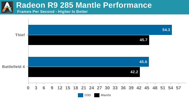
In explaining the situation, AMD tells us that this is an application level issue due to these games not being familiar with Tonga, and that this can be fixed through further patches. And ultimately if nothing else, these Tonga teething issues would be limited to these two games since they’re the only Mantle games to be released before Tonga.
The bind this puts AMD in, and why this is a bad omen for Mantle, is that if low level APIs are to take off then these kind of forward compatibility issues cannot occur. Though even high level APIs aren’t perfect – we’ve seen OS and driver updates break very old D3D and OpenGL games over time – high level APIs are forward compatible enough that virtually all games will work on newer hardware. And in the case they don’t, due to the abstraction-heavy nature of these APIs the problem and the solution are likely at the driver level. Mantle’s current state on the other hand puts the resolution in the hands of game developers, who unlike hardware vendors cannot necessarily be counted on to update their games to account for new hardware, especially given the front-loaded nature of video game sales.
For the moment Mantle is still in beta and very clearly so, with Thief and Battlefield 4 serving as proof of concept for the API. For that reason AMD still has time to contemplate the issue and ensure Mantle is more readily forward-compatible. But it’s going to be very hard justifying using Mantle if we see these kinds of regressions on non-beta drivers with games that were built against the non-beta SDK. AMD needs to ensure the shipping version of Mantle doesn’t suffer from these teething issues.
On a tangential note, this does raise the question of how well Direct3D 12 may handle the issue. By its vendor-limited nature Mantle has the opportunity to work even lower than a cross-vendor low level API like Direct3D 12, but D3D12 is still going to be low level and exposed to some of these hazards. For that reason it will be interesting to keep an eye on Direct3D development over the next year to see how Microsoft and its partners handle the issue. We would expect to see Microsoft have a better handle on forward-compatibility – in their position they pretty much have to – but if nothing else we’re curious just what it will take from game developers, API developers, and hardware developers alike to ensure that necessary level of forward-compatibility.
The Test
For the launch of the R9 285 AMD has released beta driver version 14.300.1005, which identifies itself as Catalyst 14.7 (though we suspect this will not be the final Catalyst version number). As to be expected for a launch involving a new GPU architecture, this launch driver is from a new driver branch (14.300) to account for the new hardware. With that said, based on our examination of the performance of this driver it does not appear to be significantly different than Catalyst 14.7 (14.200) for existing Radeon products.
Our R9 285 sample meanwhile is Sapphire’s R9 285 Dual-X OC. As this is a factory overclocked model, for the purposes of our testing we will be testing this card at both its factory clockspeed (965MHz/5.6GHz) and the R9 285 reference clockspeed (918MHz/5.5GHz) by underclocking our card to the appropriate clockspeeds. The bulk of our comparisons in turn will be drawn from the reference clockspeeds, but we do want to note that of the 5 R9 285 cards currently available for sale at Newegg, only a single (non-Sapphire) model is shipping without some kind of factory overclock. Consequently while we are looking to establish a reliable performance baseline, retail cards should perform a bit closer to our card’s factory overclocked performance.
| CPU: | Intel Core i7-4960X @ 4.2GHz |
| Motherboard: | ASRock Fatal1ty X79 Professional |
| Power Supply: | Corsair AX1200i |
| Hard Disk: | Samsung SSD 840 EVO (750GB) |
| Memory: | G.Skill RipjawZ DDR3-1866 4 x 8GB (9-10-9-26) |
| Case: | NZXT Phantom 630 Windowed Edition |
| Monitor: | Asus PQ321 |
| Video Cards: |
AMD Radeon R9 290 Sapphire R9 285 Dual-X OC AMD Radeon R9 280X AMD Radeon R9 280 AMD Radeon R9 270 AMD Radeon HD 7850 AMD Radeon HD 6870 NVIDIA GeForce GTX 770 NVIDIA GeForce GTX 760 NVIDIA GeForce GTX 660 NVIDIA GeForce GTX 560 Ti |
| Video Drivers: |
NVIDIA Release 340.52 WHQL AMD Catalyst 14.300.1005 Beta |
| OS: | Windows 8.1 Pro |
Metro: Last Light
As always, kicking off our look at performance is 4A Games’ latest entry in their Metro series of subterranean shooters, Metro: Last Light. The original Metro: 2033 was a graphically punishing game for its time and Metro: Last Light is in its own right too. On the other hand it scales well with resolution and quality settings, so it’s still playable on lower end hardware.
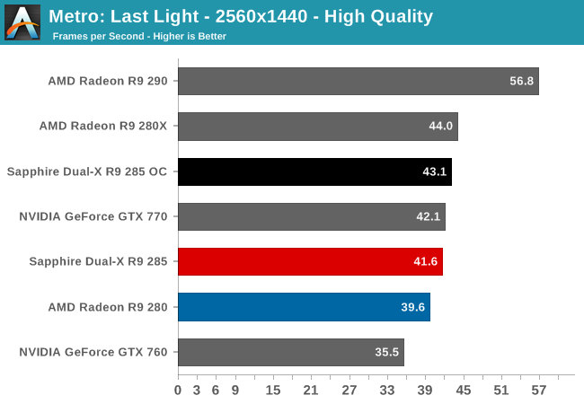
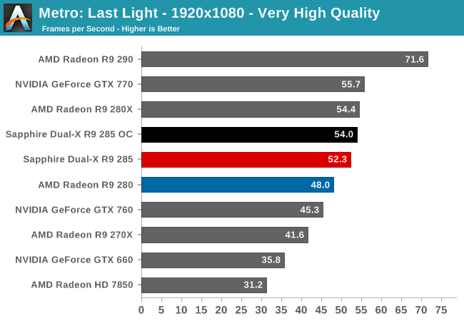
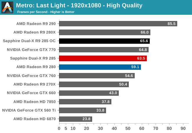
Metro, though perhaps a bit optimistic, does a decent job of setting the tone for this review. Right off the bat we can see that the R9 285 and R9 280 are performing closely to each other, with the newer R9 285 leading by 5-9%. On the whole this is greater than the average, but it’s otherwise a solid example of where the R9 285 fits into AMD’s world. In terms of design it is a lateral, but the same is also true from the resulting performance. It is not meant to – nor generally will it – perform differently from the R9 280 it replaces. R9 285 is in a nutshell an R9 280 with more features.
What this also means though is that AMD generally has the $250 price segment to themselves. In the case of Metro they have little trouble outperforming the GTX 760, and at times come close to the more expensive GTX 770. This is why Metro is a bit optimistic, since on the whole R9 285 isn’t quite enough to catch up to GTX 770.
Company of Heroes 2
Our second benchmark in our benchmark suite is Relic Games’ Company of Heroes 2, the developer’s World War II Eastern Front themed RTS. For Company of Heroes 2 Relic was kind enough to put together a very strenuous built-in benchmark that was captured from one of the most demanding, snow-bound maps in the game, giving us a great look at CoH2’s performance at its worst. Consequently if a card can do well here then it should have no trouble throughout the rest of the game.
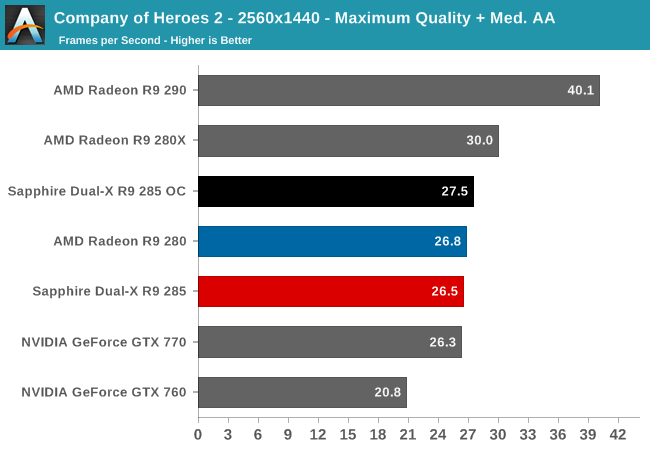
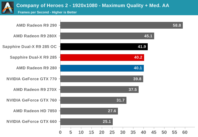
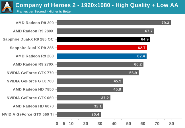
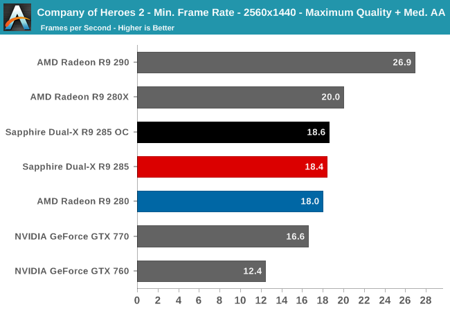
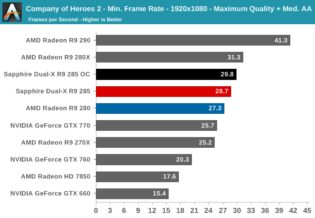
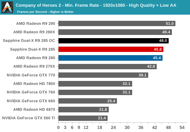
If Metro is the optimistic case then Company of Heroes 2 is the true lateral. Across all resolutions and settings the R9 285 and R9 280 are indistinct from one another, turning in average framerates within a percent or so from each other. This despite the fact that on paper the R9 280 has a 40% memory bandwidth advantage.
Bioshock Infinite
Bioshock Infinite is Irrational Games’ latest entry in the Bioshock franchise. Though it’s based on Unreal Engine 3 – making it our obligatory UE3 game – Irrational had added a number of effects that make the game rather GPU-intensive on its highest settings. As an added bonus it includes a built-in benchmark composed of several scenes, a rarity for UE3 engine games, so we can easily get a good representation of what Bioshock’s performance is like.
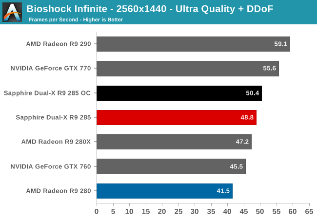
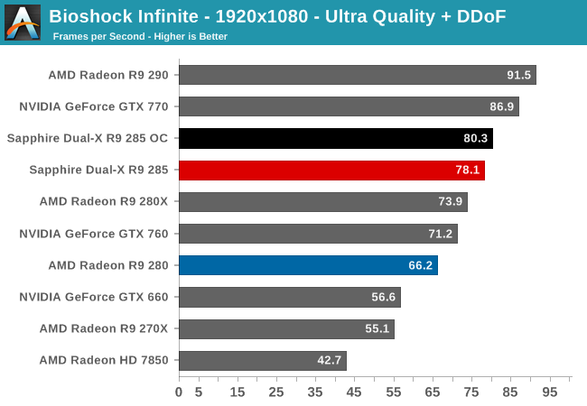
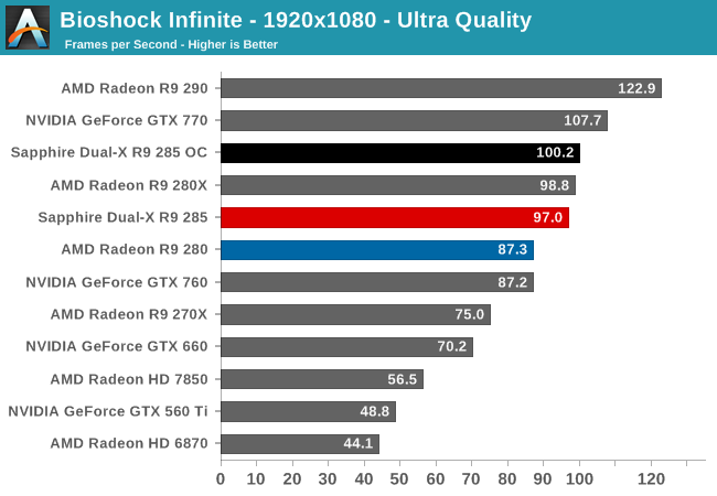
The numbers you are seeing are not an error. When it comes to Bioshock Infinite the R9 285 does amazingly well. Not only has it launched well ahead of the R9 280, but it even pulls ahead of what should otherwise be the more powerful R9 280X. Our best guess at this point is that we’re seeing an extreme case for delta color compression, where the effective bandwidth due to compression exceeds the equivalent of R9 280’s 384-bit memory bus.
Meanwhile although we haven’t talked about it much, let’s quickly go over the Dual-X OC, the factory overclocked version of this card. As Sapphire’s factory overclock is on the mild side at around 5%, the same can be said for the performance gains from it. These are solid gains, but they are not (and are not meant to be) particularly remarkable.
Battlefield 4
Our latest addition to our benchmark suite and our current major multiplayer action game of our benchmark suite is Battlefield 4, DICE’s 2013 multiplayer military shooter. After a rocky start, Battlefield 4 has finally reached a point where it’s stable enough for benchmark use, giving us the ability to profile one of the most popular and strenuous shooters out there. As these benchmarks are from single player mode, based on our experiences our rule of thumb here is that multiplayer framerates will dip to half our single player framerates, which means a card needs to be able to average at least 60fps if it’s to be able to hold up in multiplayer.
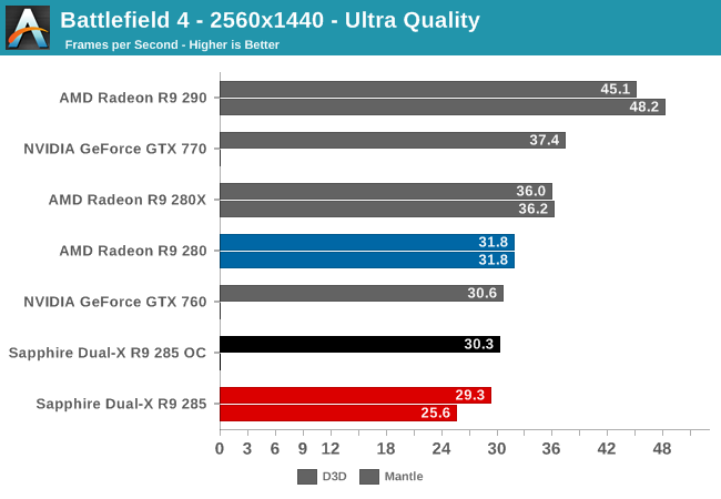
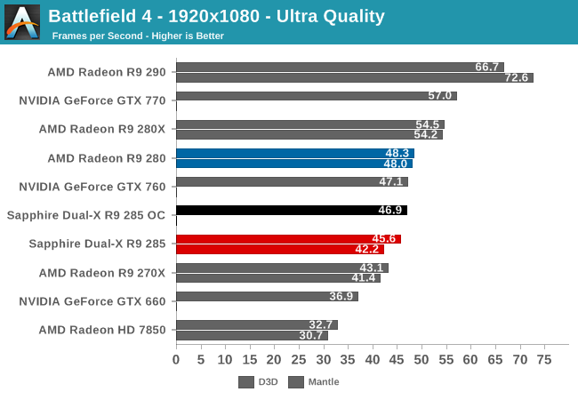
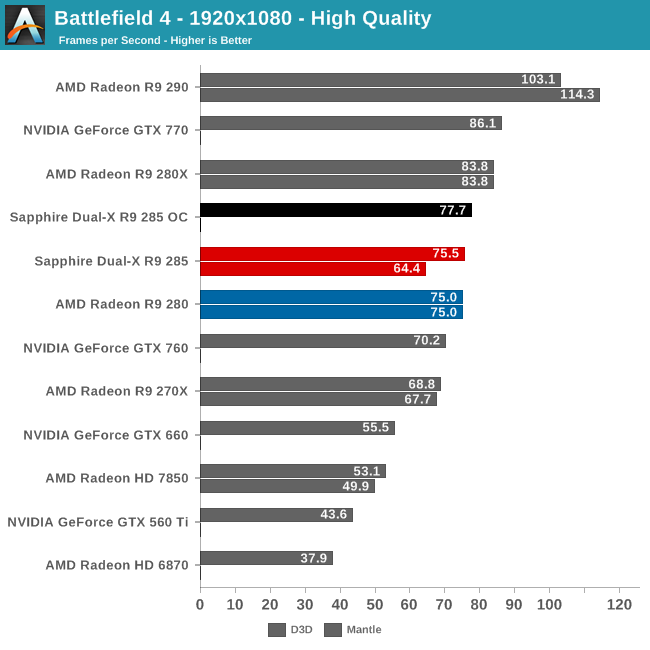
Our first Mantle-enabled game, Battlefield 4 shows the current Mantle R9 285 performance regressions front and center. At every resolution the R9 285 loses performance, sometimes remarkably so. As a result it is limited to Direct3D.
Regressions aside, I feel like Battlefield 4 is a good case for why the R9 285 needs more VRAM, or at the very least it’s not a good choice for 2560x1440. The sustained performance at 2560 is too low for this game, and the performance loss compared to the 3GB R9 280 appears to be a direct result of VRAM pressure. If the R9 285 had more VRAM, I suspect it would reach parity with the R9 280, especially given what happens at 1080p with High settings.
In any case, this is also the first game where the R9 285 trades blows with the GTX 760 rather than taking a distinct lead. With both cards limited to Direct3D, both cards are also returning similar performance. Which for R9 285 and its higher price tag is essentially a loss.
Crysis 3
Still one of our most punishing benchmarks, Crysis 3 needs no introduction. With Crysis 3, Crytek has gone back to trying to kill computers and still holds “most punishing shooter” title in our benchmark suite. Only in a handful of setups can we even run Crysis 3 at its highest (Very High) settings, and that’s still without AA. Crysis 1 was an excellent template for the kind of performance required to drive games for the next few years, and Crysis 3 looks to be much the same for 2014.
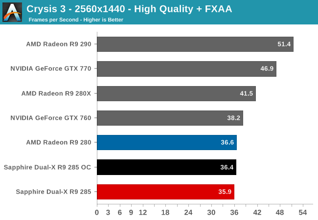
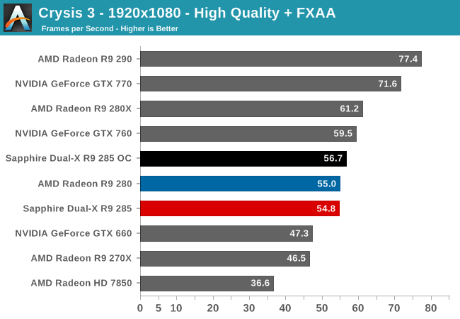
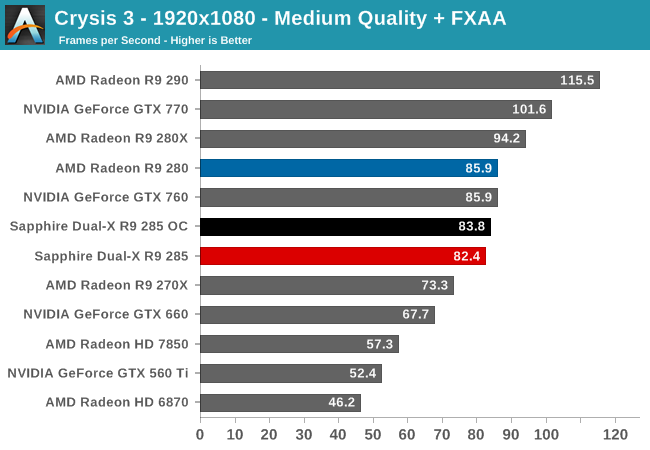
Crysis 3 ends up being another lateral for AMD, with the R9 285 and R9 280 virtually tied at 2560x1440 and 1920x1080 with High quality settings. Only at 1920x1080 do we see them pull apart, with the R9 280 taking a mild 4% lead. On a side note, since this is our game of choice for measuring power consumption, this is especially handy as it means we have equalized performance from the start, making power consumption at the wall less affected by performance differences.
Meanwhile as this is a game that generally favors NVIDIA cards these days, it comes as little surprise to see the R9 285 trailing the GTX 760 by 4 to 8%. The factory overclocked version of this card fares a little better in that respect, but it’s not quite enough to close that large of a gap.
Crysis: Warhead
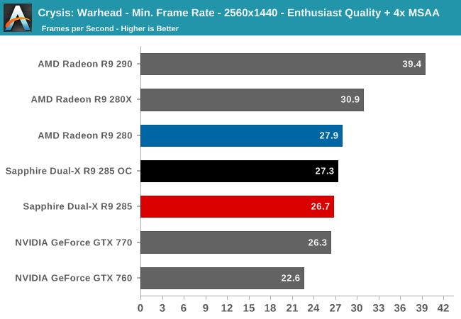
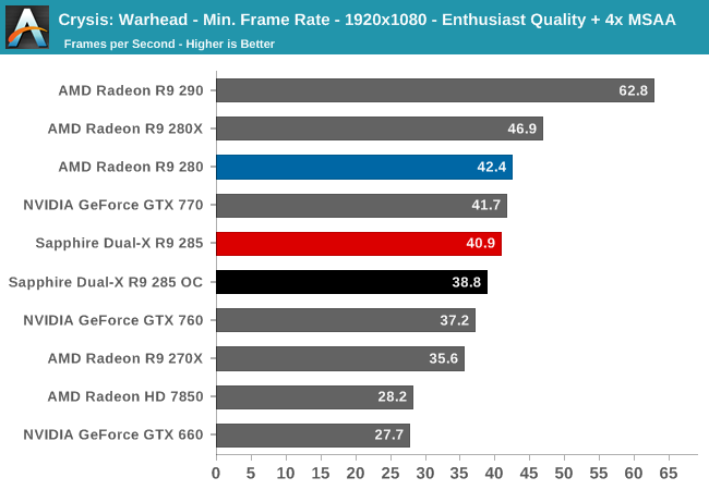
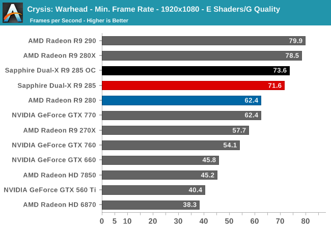
Up next is our legacy title for 2014, Crysis: Warhead. The stand-alone expansion to 2007’s Crysis, at over 5 years old Crysis: Warhead can still beat most systems down. Crysis was intended to be future-looking as far as performance and visual quality goes, and it has clearly achieved that. We’ve only finally reached the point where single-GPU cards have come out that can hit 60fps at 1920 with 4xAA, never mind 2560 and beyond.
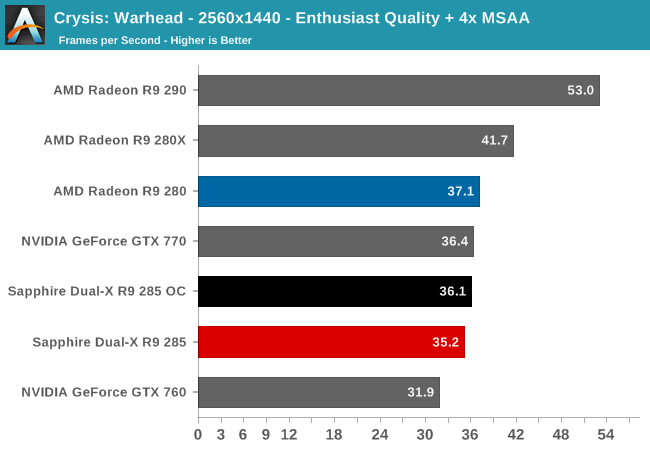
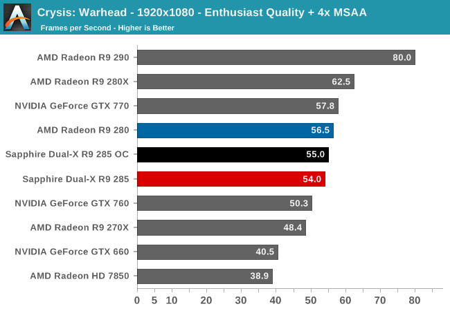
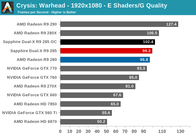
Crysis Warhead is one of the few cases where R9 285 tends to regress, with the R9 280 leading the R9 285 by around 5% at our highest settings. Interestingly, the tables turn at the lower quality settings and R9 285 regains the lead, but overall this is mostly a wash.
Total War: Rome 2
The second strategy game in our benchmark suite, Total War: Rome 2 is the latest game in the Total War franchise. Total War games have traditionally been a mix of CPU and GPU bottlenecks, so it takes a good system on both ends of the equation to do well here. In this case the game comes with a built-in benchmark that plays out over a forested area with a large number of units, definitely stressing the GPU in particular.
For this game in particular we’ve also gone and turned down the shadows to medium. Rome’s shadows are extremely CPU intensive (as opposed to GPU intensive), so this keeps us from CPU bottlenecking nearly as easily.
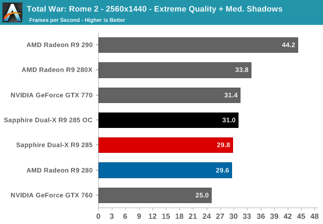
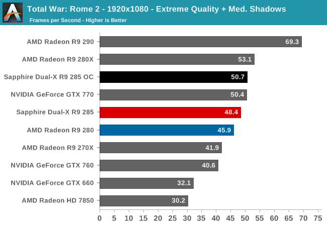
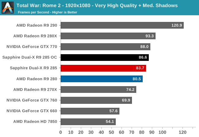
With Total War: Rome 2, we’re back to a pattern of the R9 285 performing slightly better than the R9 280 it replaces. At 5% faster it’s a small difference, but it helps to secure the card’s overall lead in the averages. At this point we can only assume that we’re once again seeing color compression in action, though as an RTS with tessellation we can’t entirely rule out some of those geometry improvements playing a part too. Whatever the reason, it puts AMD in a good spot competitively. The R9 285 is once again within striking distance of the GTX 770, all the while leaving the GTX 760 behind by a rather unexpected 20%.
Thief
Our newest addition to our benchmark suite is Eidos Monreal’s stealth action game, Thief. Set amidst a Victorian-era fantasy environment, Thief is an Unreal Engine 3 based title which makes use of a number of supplementary Direct3D 11 effects, including tessellation and advanced lighting. Adding further quality to the game on its highest settings is support for SSAA, which can eliminate most forms of aliasing while bringing even the most powerful video cards to their knees.
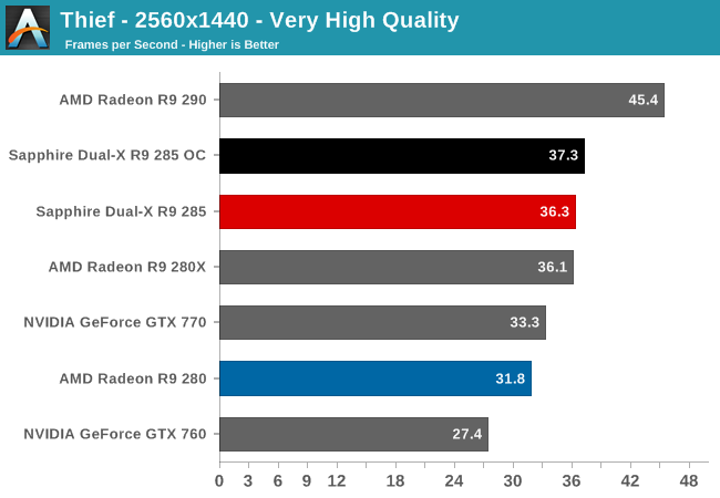
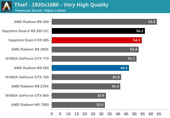
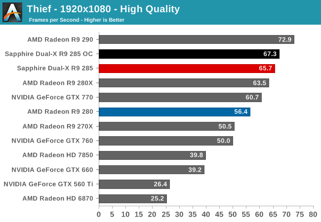
With Mantle’s current performance regressions on R9 285, Thief is best played using the Direct3D renderer. In this case we have another situation where the R9 285 is doing unexpectedly well against the R9 280 and even R9 280X, edging out the latter in all three benchmarks. Thief does make use of SSAA at High and Very High qualities, so we may be seeing another case of color compression working its magic since the oversampling should improve image compressibility. Meanwhile for Sapphire’s factory overclock, the extra bandwidth savings offers some additional legroom to pull ahead of the stock card. This gives Sapphire’s overclock a roughly 4% performance advantage.
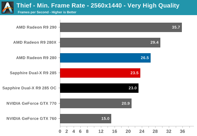
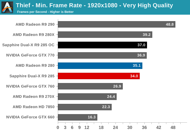
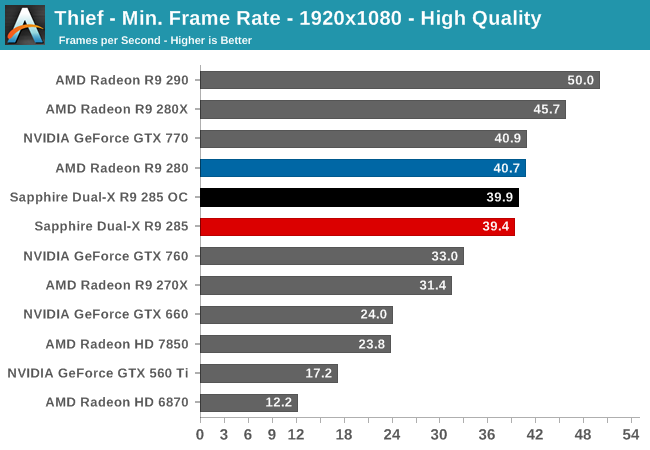
However looking at minimum framerates, Thief is also another good example to question whether 2GB is really enough VRAM. Strong average framerates give way to inferior minimums, especially at 2560. This is one of the reasons we believe that the R9 285 is not a good match for 2560 in the long term.
GRID 2
The final game in our benchmark suite is also our racing entry, Codemasters’ GRID 2. Codemasters continues to set the bar for graphical fidelity in racing games, and with GRID 2 they’ve gone back to racing on the pavement, bringing to life cities and highways alike. Based on their in-house EGO engine, GRID 2 includes a DirectCompute based advanced lighting system in its highest quality settings, which incurs a significant performance penalty but does a good job of emulating more realistic lighting within the game world.
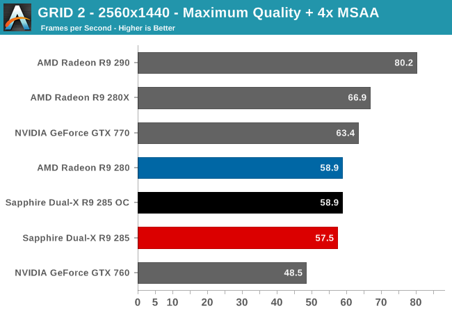
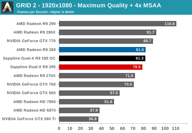
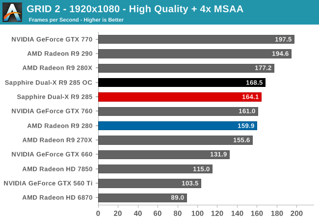
Our final game sees the R9 285 and R9 280 close together, with cards either coming close to tying or trading the lead depending on the specific settings we use. Overall the use of color compression doesn’t seem to quite make up for the bandwidth loss, with the R9 280 generally taking a very small lead. For AMD in general however this is another strong game. The R9 285 has no trouble outperforming the GTX 760 at Maximum quality.
Synthetics
As always we’ll also take a quick look at synthetic performance. As we briefly discussed in our look at the GCN 1.2 architecture these tests mainly serve as a canary for finding important architectural changes, and one of these tests in particular has been significantly impacted by AMD’s newest round of architectural improvements.
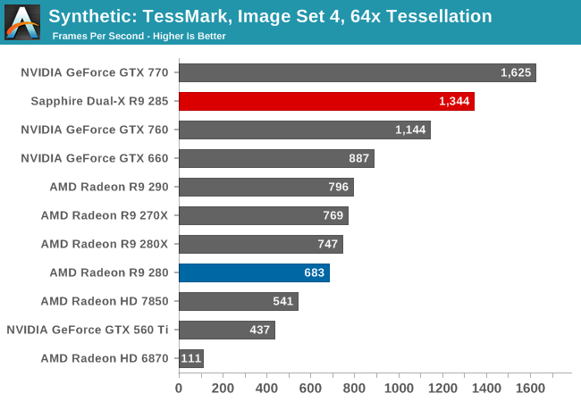
At the x64 tessellation factor we see the R9 285 spit out 134fps, or equivalent to roughly 1.47B polygons/second. This is as compared to 79fps (869M Polys/sec) for the R9 290, and 68fps (748M Polys/sec) for the R9 280. One of the things we noted when initially reviewing the R9 290 series was that AMD’s tessellation performance didn’t pick up much in our standard tessellation benchmark (Tessmark at x64) despite the doubling of geometry processors, and it looks like AMD has finally resolved that with GCN 1.2’s efficiency improvements. As this is a test with a ton of small triangles, it looks like we’ve hit a great case for the vertex reuse optimizations.
Moving on, we have our 3DMark Vantage texture and pixel fillrate tests, which present our cards with massive amounts of texturing and color blending work. These aren’t results we suggest comparing across different vendors, but they’re good for tracking improvements and changes within a single product family.
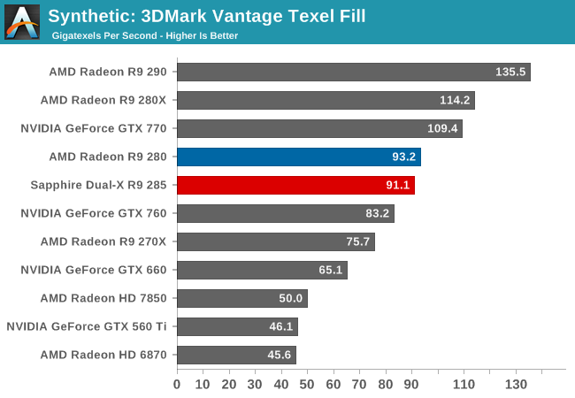
With AMD maintaining their same texture units and same tex:FP32 ratio for Tonga, the end result is that R9 285’s texturing performance is virtually identical to R9 280’s. Ignoring any possibility of caching or bandwidth bottlenecking for the moment, R9 285 can push texels just as well as R9 280 could.
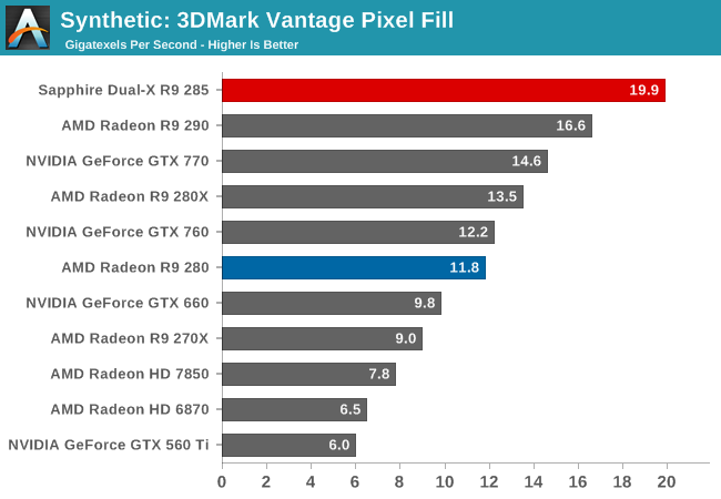
Unlike our texel test, AMD’s delta color compression technology introduced on GCN 1.2 has an incredible impact on R9 285’s pixel throughput. This pixel test is normally memory bandwidth bound, providing something that approaches a best case scenario for AMD’s compression technology. As a result despite possessing nearly 30% less memory bandwidth than the R9 280, the R9 285 tops our charts at 19.9 GPix/sec, blowing past the R9 280 by 68%. Even the R9 290 with its 512-bit memory bus and doubled ROP count still falls short here by over 3GPix/sec, or 16%.
This benchmark in a nutshell is why AMD can deliver the average performance of the Tahiti based R9 280 without Tahiti’s memory bandwidth. By improving their color compression to this point AMD can significantly reduce their memory bandwidth requirements on GCN 1.2, allowing them to do more with less. In real games the result won’t be anywhere near this remarkable since this is a pure pixel fillrate test, but it goes to show that AMD has been able to neutralize their memory bandwidth deficit in graphics workloads.
Compute
Jumping into compute, our expectations regarding compute performance are going to be a mixed bag. On the one hand as part of the newer GCN 1.2 architecture AMD has been doing some tweaking under the hood, but on the other hand the most important aspects of the architecture – the memory model and thread execution – are not fundamentally different from the GCN 1.0 R9 280. As a result we’re not necessarily expecting to find any performance leaps here but there is the possibility that we will find some along the way.
As always we’ll start with LuxMark2.0, the official benchmark of SmallLuxGPU 2.0. SmallLuxGPU is an OpenCL accelerated ray tracer that is part of the larger LuxRender suite. Ray tracing has become a stronghold for GPUs in recent years as ray tracing maps well to GPU pipelines, allowing artists to render scenes much more quickly than with CPUs alone.
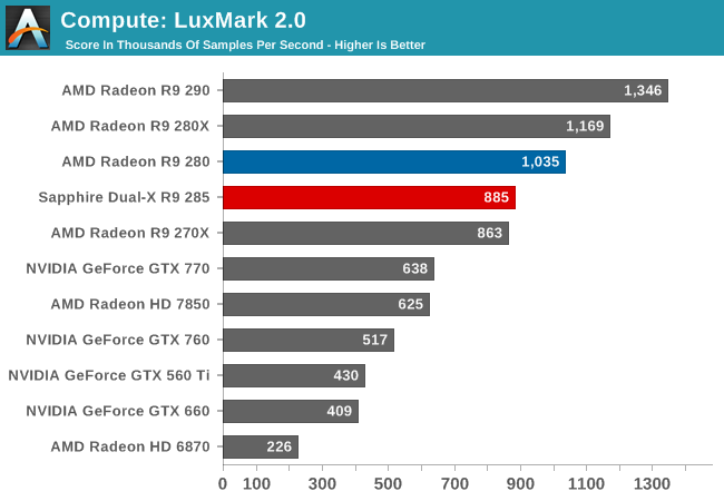
Right off the bat we find an unexpected regression in performance with LuxMark. All things considered we would expect the R9 285 to score similarly to the R9 280 given their nearly identical theoretical FP32 throughput, similar to what we’ve seen in our gaming benchmarks. Instead we have the R9 285 trailing its predecessor by 15%, and coming very close to tying the otherwise much slower R9 270X. Given that this is a new architecture there are a few possibilities here including a lack of OpenCL driver optimizations on AMD’s part, though we can’t entirely rule out bandwidth either since ray tracing can burn up bandwidth at times. Tonga is after all first and foremost a graphics product, and AMD’s memory bandwidth saving compression technology is similarly designed for graphics and not compute, meaning the R9 285 doesn’t have much to make up for the loss of bandwidth in compute tasks versus the R9 280.
In any case, even with R9 285 lagging the R9 280, it’s otherwise a strong showing for AMD. AMD cards overall perform very well on this benchmark compared to NVIDIA’s offerings, so the R9 285 has no trouble shooting well past the GTX 760.
Our 2nd compute benchmark is Sony Vegas Pro 12, an OpenGL and OpenCL video editing and authoring package. Vegas can use GPUs in a few different ways, the primary uses being to accelerate the video effects and compositing process itself, and in the video encoding step. With video encoding being increasingly offloaded to dedicated DSPs these days we’re focusing on the editing and compositing process, rendering to a low CPU overhead format (XDCAM EX). This specific test comes from Sony, and measures how long it takes to render a video.
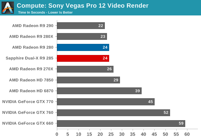
Unlike LuxMark, we aren’t seeing a performance gain nor a regression here. The R9 285 is every bit as fast as the R9 280. Meanwhile as has consistently been the case in this benchmark, all of AMD’s cards are well ahead of our NVIDIA cards.
Our 3rd benchmark set comes from CLBenchmark 1.1. CLBenchmark contains a number of subtests; for our standard benchmark suite we focus on the most practical of them, the computer vision test and the fluid simulation test. The former is a useful proxy for computer imaging tasks where systems are required to parse images and identify features (e.g. humans), while fluid simulations are common in professional graphics work and games alike.
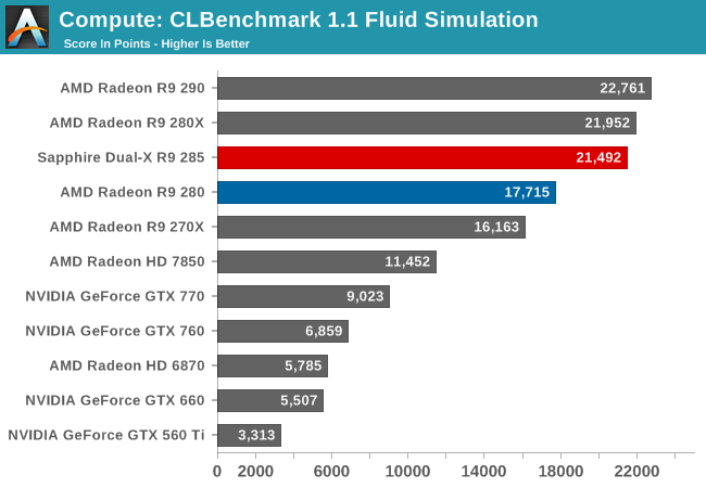
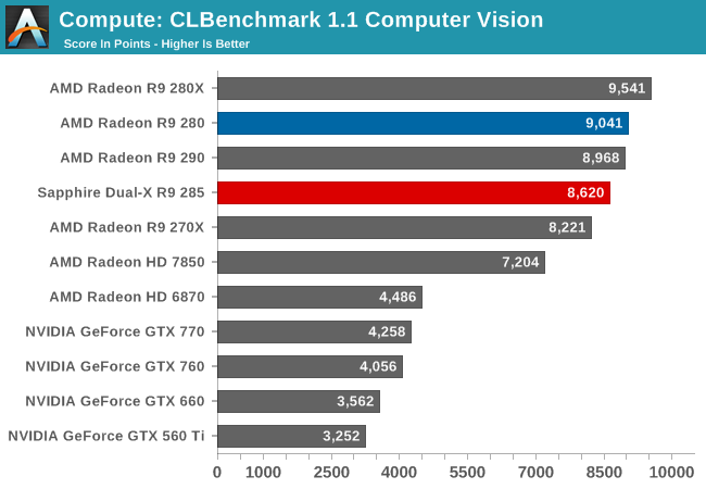
Depending on which subtest we’re looking at, the R9 285 either outperforms or trails the R9 280. The fluid simulation subtest finds the R9 285 performing just shy of the more powerful R9 280X, while the R9 285 comes up short of the R9 280 in computer vision. Computer vision is the more bandwidth sensitive benchmark of the two, so it follows that it’s the benchmark more likely to be influenced by the loss of raw memory bandwidth. Otherwise the R9 285’s strong showing in the fluid simulation is unexpected, and given what we know we’re at a bit of a loss to explain it.
Looking at the broader picture, this is yet another test where AMD’s cards do well against NVIDIA’s non-compute cards. Overall the R9 285 is 2-3x faster than the GTX 760 here.
Moving on, our fourth compute benchmark is FAHBench, the official Folding @ Home benchmark. Folding @ Home is the popular Stanford-backed research and distributed computing initiative that has work distributed to millions of volunteer computers over the internet, each of which is responsible for a tiny slice of a protein folding simulation. FAHBench can test both single precision and double precision floating point performance, with single precision being the most useful metric for most consumer cards due to their low double precision performance. Each precision has two modes, explicit and implicit, the difference being whether water atoms are included in the simulation, which adds quite a bit of work and overhead. This is another OpenCL test, utilizing the OpenCL path for FAHCore 17.
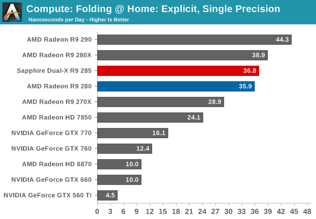
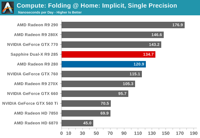
When it comes to single precision the R9 285 edges out the R9 280, though not significantly so. R9 285 still seemingly benefits from some of the GCN 1.2 architectural optimizations, but not to the same extent we’ve seen in other benchmarks.
Overall AMD’s GCN cards are a strong performer in this benchmark and the R9 285 is no exception. GTX 760 trails R9 285 when it comes to implicit single precision, and is blown away in the explicit single precision benchmark.
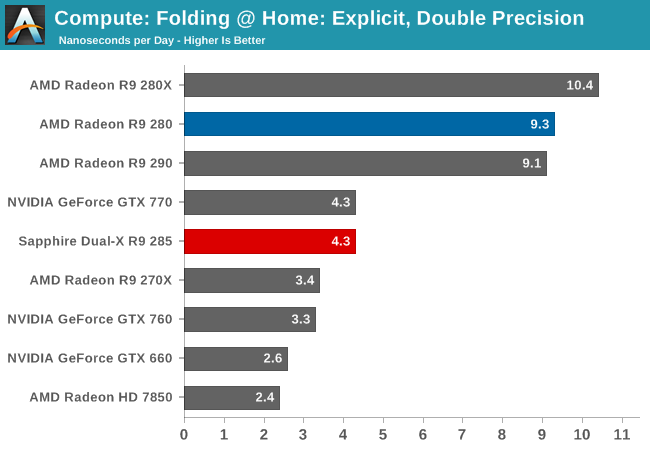
Meanwhile for double precision the R9 285 falls well behind the R9 280. Since Tonga is not designed to pull double-duty as a graphics and high performance compute GPU like Tahiti was, Tonga is configured for 1/16 rate double precision performance, 1/4 the rate of the more powerful Tahiti. As a result it can never keep up with the R9 280 in a double precision workload. Consequently AMD and the R9 285 still have a lead in F@H with double precision, but not to the degree we’ve seen elsewhere. The R9 285 is only about 30% faster than the GTX 760 here.
Wrapping things up, our final compute benchmark is an in-house project developed by our very own Dr. Ian Cutress. SystemCompute is our first C++ AMP benchmark, utilizing Microsoft’s simple C++ extensions to allow the easy use of GPU computing in C++ programs. SystemCompute in turn is a collection of benchmarks for several different fundamental compute algorithms, with the final score represented in points. DirectCompute is the compute backend for C++ AMP on Windows, so this forms our other DirectCompute test.
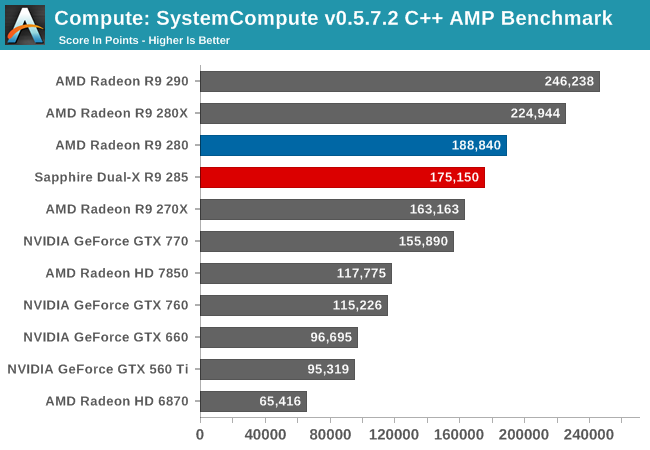
SystemCompute exposes another case where the R9 285 comes up short compared to the R9 280, though only slightly. AMD’s latest card can deliver 93% of the performance of an R9 280, and most likely it’s suffering just a bit from the reduction in memory bandwidth. Otherwise it’s still more than 50% ahead of the GTX 760 and still comfortably ahead of the more powerful GTX 770.
Power, Temperature, & Noise
As always, last but not least is our look at power, temperature, and noise. Next to price and performance of course, these are some of the most important aspects of a GPU, due in large part to the impact of noise. All things considered, a loud card is undesirable unless there’s a sufficiently good reason – or sufficiently good performance – to ignore the noise.
So far we’ve seen AMD take a lateral when it comes to gaming performance, resulting in R9 285 keeping up with R9 280 rather consistently. It is clear that AMD has specifically intended for R9 285 to deliver R9 280-like gaming performance, so that is exactly what has happened above the hood.
Under the hood however there are not one but two generations of GCN upgrades to account for, which have the potential to significantly alter the power/temp/noise characteristics of the video card. Compared to the GCN 1.0 based Tahiti GPU, GCN 1.2 introduces not only AMD’s radically improved PowerTune implementation, but it also introduces their delta color compression technology that cuts down on the size of the memory bus and the resulting number of RAM chips needed on a completed card. As a result R9 285 can at times perform quite differently from R9 280, especially when it comes to power.
| Radeon R9 285 Voltages | ||||
| Saph. 285 DXOC Load | Saph. 285 DXOC Idle | AMD R9 280 Load | ||
| 1.15V | 0.9V | 1.1V | ||
Starting with voltages, we want to quickly remind everyone that as of GCN 1.1 AMD no longer provides a way of easily reading a GPU’s desired VID, and instead we get the real voltage as reported through the card’s sensors. In this case we’re taking our voltages from LuxMark 2.0, which offers a consistent workload that is strenuous enough to max out the GPU, but light enough that virtually every GPU should be able to boost to its maximum turbo bin. In any case these aren’t going to be the maximum voltages for any given card, but they should be close.
For our Sapphire R9 285 Dual-X OC, we find that our card stabilizes at 1.15V under load and idles at 0.9V. Compared to our R9 280 this appears to be a higher load voltage and idle voltage, but it must be noted that the 280 is reporting its VID instead of its actual voltage.
Meanwhile as GCN 1.2 cards implement the same fine-grained PowerTune support that was first pioneered in GCN 1.1, we want to take a look at average clockspeeds as well. With all of AMD’s modern GCN 1.1+ cards, AMD and most of their partners are advertising the cards by their boost clockspeed. So it’s helpful to see if these cards can maintain these clockspeeds throughout. In practice the potential for throttling is much greater in thermally constrained situations (blowers, e.g. R9 290) than it is for open air coolers, but there is still the potential for hitting situations where we throttle based on power consumption.
| Radeon R9 285 Average Clockspeeds | ||||
| Saph DXOC (Stock) | Saph DXOC (Fact. OC) | |||
| Boost Clock | 918MHz | 965MHz | ||
| Metro: LL |
918MHz
|
965MHz
|
||
| CoH2 |
918MHz
|
965MHz
|
||
| Bioshock |
918MHz
|
963MHz
|
||
| Battlefield 4 |
918MHz
|
965MHz
|
||
| Crysis 3 |
918MHz
|
965MHz
|
||
| Crysis: Warhead |
918MHz
|
965MHz
|
||
| TW: Rome 2 |
918MHz
|
965MHz
|
||
| Thief |
918MHz
|
965MHz
|
||
| GRID 2 |
918MHz
|
965MHz
|
||
The long and short of it is that the R9 285 Dual-X has no trouble maintaining its 918MHz clockspeed when underclocked. Though it doesn’t affect the averages we do see some very minor fluctuations in clockspeed (an errant 916/917MHz here and there), which is likely due to AMD’s clockspeed governing mechanism rather than any kind of power or temperature throttle. Note that even under FurMark, our worst case (and generally unrealistic) test, the card only falls by less than 20Mhz to 900MHz sustained.
Otherwise if we bring the Dual-X back to its factory overclocked speeds, we find that it has no problem maintaining 965MHz, outside of the exception of Bioshock which fluctuated frequently enough that it averaged a mere 963Mhz.
Unfortunately this means we have also been unable to determine the base clockspeed for these cards. Even holding back cooling and reducing the power target, the R9 285 doesn’t seem to have a GPU clockspeed floor, unlike the Hawaii based R9 290 series.
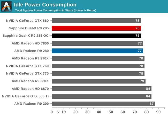
At this point outside of cards that are design deficient in some way or another, idle power is unremarkable. Sapphire’s R9 285 Dual-X puts up with the best, with the 2W gain over the R9 280 likely coming from the reduced VRAM capacity.
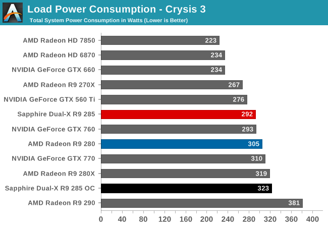
Moving on to load power consumption under Crysis 3 we find that power consumption has been reduced compared to the R9 280, but not remarkably so. Despite the much lower official TBP of 190W versus 250W for the R9 280, the actual difference (for virtually equivalent performance) is 13W of savings at the wall. What this tells us is that despite the PowerTune changes, the R9 285 is sustaining power consumption not all that far removed from the R9 280. In practice the R9 280 was unlikely to be drawing near 250W under a gaming workload, so in this case the 190W value for the R9 285 is not all that far removed from the R9 280. The remaining difference is due to the VRAM reduction and some power efficiency gains in Tonga.
On the other hand power consumption for the Dual-X when using its factory overclock launches ahead. The slight increase in performance under Crysis 3 from this overclock will increase the load on the CPU, but only slightly. The rest comes from the power required to hit and sustain the higher clockspeeds of Sapphire’s overclock. As a result we’re looking at power consumption near the level of an R9 280X.
Meanwhile to make a quick GTX 760 comparison, AMD and NVIDIA are virtually tied. At 292W versus 293W, these cards are drawing virtually identical amounts of power. However the GTX 760 ultimately has the efficiency edge, as it delivers better performance under Crysis 3 than the R9 285 does (though in other games the tables could of course turn).
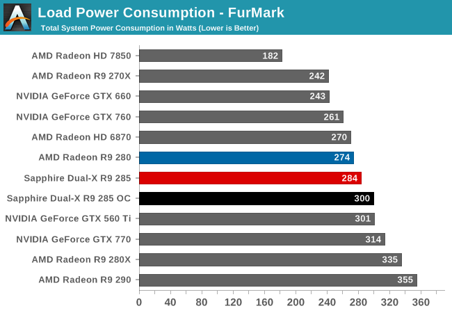
Surprisingly, under Furmark the situation is actually reversed. Instead of the R9 285 beating the R9 280, we’re actually seeing it draw 10W more power despite the lower TBP. Though seemingly nonsensical, in practice this is the newer iteration of PowerTune doing a better job of homing in on the card’s 190W limit. This is a situation the coarse PowerTune implementation on R9 280 would have trouble with, causing it to have to back off on clockspeeds much more severely, and ultimately drawing less power than its limit would truly allow.
The end result is something of a wash. The R9 285 is not drawing significantly more or less power than the R9 280, all the while delivering similar performance. In that context we can say that as a result, power efficiency has not meaningfully changed compared to the R9 280.
Finally to make one more GTX 760 comparison, this illustrates that while AMD can generally beat the GTX 760’s performance, it also comes at the cost of maximum power consumption. At least when faced with a worst case scenario, the R9 285 is going to be drawing about 20W more at the wall.
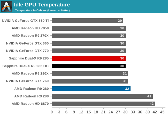
When it comes to idle temperatures, Sapphire’s Dual-X cooler is among the best. 30C at idle is average in the pack only because so many other coolers are as equally able at idle.
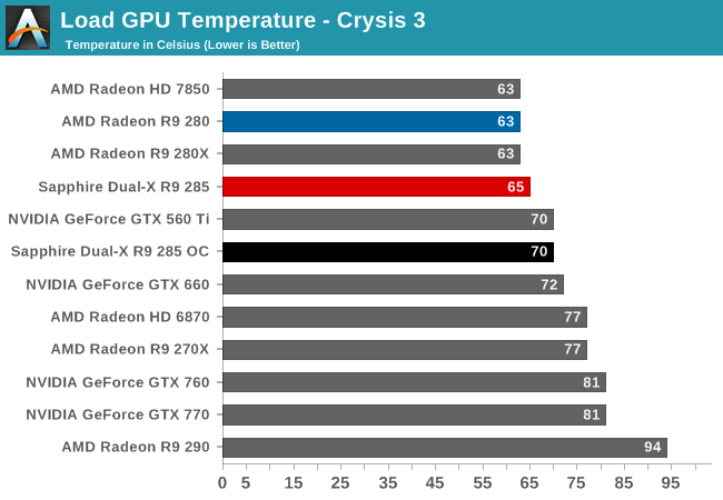
Earlier we mentioned that the Dual-X cooler is probably a bit overpowered for a 190W card, and here we can see why. Under Crysis 3 our card maxes out at a relatively chilly 65C, and even with the factory overclock only pushes to 70C. Sapphire’s card clearly has no problem keeping itself cool.
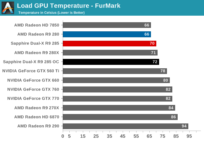
The greater load from FurMark causes temperatures to rise a bit more, but not exceptionally so. Even under this most strenuous of tests we’re topping out at 70C with reference clockspeeds, or 72C with the factory overclock. So long as Sapphire can hit these temperatures without generating too much noise then they’re golden (or blue, as the case may be).
I would also point out at this time that while the R9 285 Dual-X is significantly cooler than the GTX 760, we’re comparing an open air cooler to a blower. All things considered this is exactly the situation where the open air cooler will be the stronger performer. But it comes at the tradeoff of not being able to directly expel all of its waste heat.
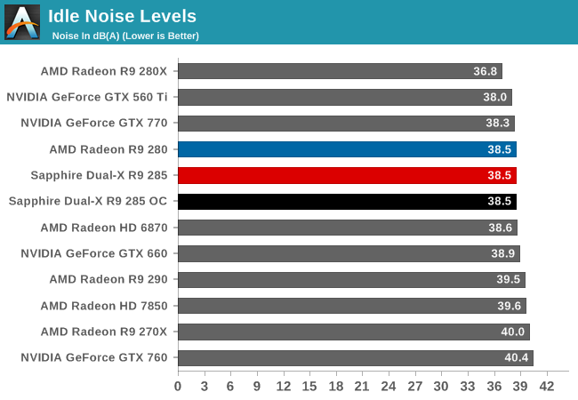
Much like idle temperatures, idle noise levels are looking quite good for Sapphire’s Dual-X cooler. There are a handful of cards that can drop below even 38.5dB, but at this point we’re quickly approaching the overall noise floor.
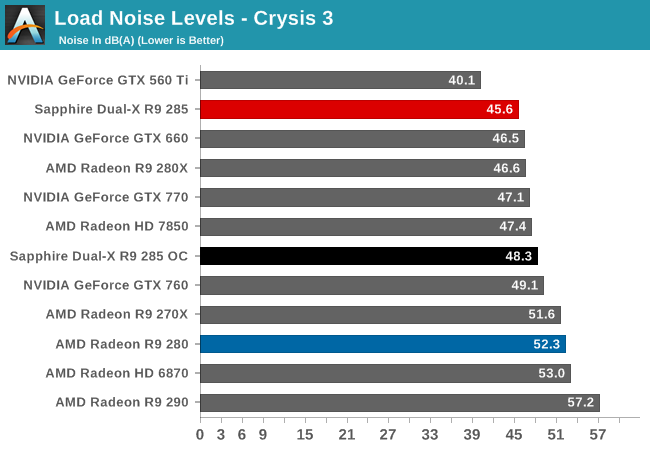
Already doing very well for themselves when it comes to load temperatures, load noise only makes Sapphire’s R9 285 Dual-X look even better. When we underclock it to stock speeds we’re only getting 45.6dB under load, quieter than any Tahiti card, Hawaii card, Pitcairn card, or Kepler card. Only the old GTX 560 Ti (which was impressively overbuilt) can sustain load noises lower than 45.6dB.
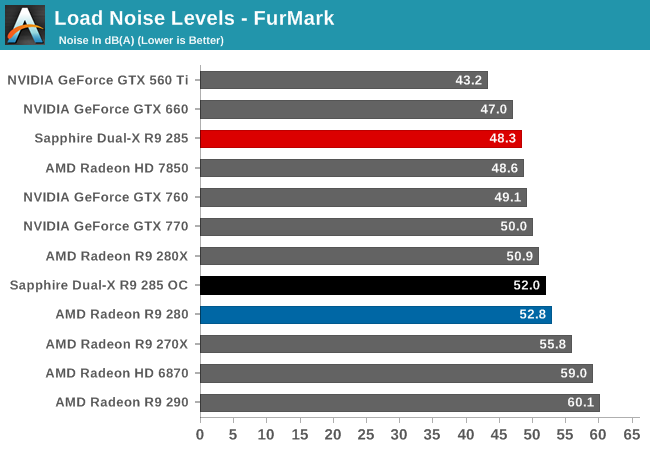
As was the case with temperatures, FurMark also drives up the load noise levels, but not especially so. Even with this additional heat the R9 285 tops out at 48.3dB, staying comfortably under the 50dB level and trailing only the much less powerful GTX 660 and GTX 560 Ti.
Meanwhile when looking at the R9 285 Dual-X with its factory overclock enabled, we unsurprisingly see an increase in noise from the additional heat generated by the overclock. The total penalty for the overclock is 3-4dB, which is a not-insignificant increase in noise. I feel like Sapphire really hit their sweet spot for balancing noise with performance at stock, so the factory overclock deviates from that some. Overall these noise levels are still well within reason, but they’re now middle of the pack instead of near the head of the pack.
Speaking of Sapphire cards, it’s interesting to compare and contrast the R9 285 with our R9 280, which is also a Sapphire card using an identical cooler. Compared to the R9 280, for the R9 285 Sapphire has found a better balance between temperature and noise. The R9 280 could pull off slightly better temperatures, but it was always above 52dB of noise under load as a result.
Ultimately excluding the vender-specific factors, our look at power, temperature, and noise tells us that much like the R9 285’s gaming performance, the R9 285’s power/temp/noise performance is a lateral move for AMD. Performance hasn’t significantly changed and neither has power, which really helps to distill the essence of R9 285 down to its improved GCN 1.2 feature set. Which in this case in particular means features such as the much finer-grained clockspeeds offered by PowerTune.
Final Thoughts
Throughout our entire review we’ve been calling the Radeon R9 285 a lateral for AMD, and as we’ve seen in our results this is for a good reason. Despite all of the architectural and feature changes between the R9 285 and its R9 280 predecessor – everything from the GCN 1.2 feature set to color compression to the smaller VRAM pool – the R9 285 truly is a lateral for AMD. At the end of the day it brings a very minor 3-5% performance increase over the R9 280 with virtually no change in price or power consumption. Functionally speaking it’s just an R9 280 with more features.
To that end laterals like the R9 285 are currently an oddity in the video card landscape, but it’s something that we should expect to see more of in the future. As GPU architectures mature and the rate of progress on new manufacturing nodes continues to slow, we no longer have the same yearly or even biennial shakeup in the GPU landscape. Tahiti at this point is nearly three years old and is still going strong, and the 28nm process it’s built on is going to be with us for a while yet. Which means newer generations of video cards are going to be farther apart, and a new opening is created for smaller refreshes such as Tonga and GCN 1.2.
From a feature standpoint then, Tonga and the underlying GCN 1.2 architecture is a small but nonetheless impressive iteration on what AMD has already done with GCN 1.1. I think it’s going to take some time to really see the impact of the newer ISA, but the improvements to geometry performance and color compression are very immediate and very potent. The fact that AMD has been able to offset a roughly 30% bandwidth reduction just through the use of color compression is certainly a feather in AMD’s cap, and this is only going to get more important over time as we have hit a wall on GDDR5 clockspeeds and memory bus widths, especially on the high-end. Meanwhile AMD’s upgrades to their video decode and encode capabilities should not go unnoticed; AMD has finally caught up to NVIDIA on video decoding – especially in 4K H.264 compatibility – and the ability to encode 4K H.264 in hardware may yet prove advantageous.
As for R9 285’s customer base and its competition, AMD’s product positioning continues to be straightforward. AMD has continued to undercut NVIDIA on a price/performance basis across the entire Radeon 200 family, and R9 285 upholds this tradition. If we’re just looking for the card with the best performance for the price, the R9 285 solidly outperforms NVIDIA’s GTX 760 by 12-15%, and it’s by no mistake that GTX 760 prices have slid in the last week in response.
The ramification of this is that AMD no longer holds a real price/performance advantage – the price gap just about matches the performance gap at this point – but this does mean that the R9 285 is in its own little performance niche as a more powerful but more expensive video card compared to the GTX 760. The end result is that we have a tossup: you could buy either and be satisfied for the price.
AMD’s lineup on the other hand is a bit more volatile and will remain so until R9 280 stocks run out. With AMD’s partners selling off their remaining R9 280 cards at clearance sale prices, the R9 280 is a very strong value proposition at $210-$220, offering virtually identical performance to the R9 285 for $40 less. However like all GPU discontinuation clearance sales this situation will be fleeting, and at some point R9 280 will go away and $250 R9 285 will be the status quo. In the meantime however one is also left with the harder choice of picking price or features; the R9 285 has a few features that in the long run are going to make a difference, such as full support for DisplayPort Adaptive-Vsync (Freesync) and a 4K capable video decoder, but whether that’s worth a $40 premium is going to be very situational if not outright difficult to justify.
All things considered then the R9 285 is a solid card, however I remain unconvinced that AMD has equipped it with the right amount of memory. From a GPU performance perspective I feel that AMD is overshooting in promoting the R9 285 as a 2560x1440 card, as the raw performance to run at that resolution with high quality settings just isn’t there, but even as a 1080p card 2GB for $250 is tough to swallow and is made all the worse by the 3GB R9 280. 2GB for 1080p is enough for now, but whether that will still be true in 2-3 years seems unlikely. A 4GB R9 285 would be a much safer bet as a result, however it doesn’t necessarily follow that it would be worth a price premium at this time.
Switching gears for a moment, second-tier cards like the R9 285 are often not the strongest showing for a new GPU like Tonga. Given all the similarities between Tonga and Tahiti, it seems like it’s only a matter of time until R9 280X gets the Tonga treatment. And even though it would be the second Tonga card, I think it could prove to be just as interesting as the R9 285 (if not more so), as it will give us a chance to see just what an unrestricted Tonga product can do. To that end, I hope AMD doesn’t leave us waiting too long to release a fully enabled Tonga SKU.

