Original Link: https://www.anandtech.com/show/838
AMD's Hammer Architecture - Making Sense of it All
by Anand Lal Shimpi on October 23, 2001 2:57 AM EST- Posted in
- CPUs
When AMD first revealed the K7 architecture at the Microprocessor Forum in 1998 who would have thought that the Athlon would turn out to be this successful? This two-year old micro architecture from AMD has been able to dethrone Intel's Pentium III and make many users think twice before adopting the Pentium 4 platform. Today the Athlon XP boasts the highest desktop performance of any x86 processors and it does so based on the K7 architecture that was originally introduced at MPF.
Fast forwarding to the present day; AMD has gained a significant amount of market share and at this year's MPF the underdog in green introduced the details of their next-generation microprocessor architecture under the "Hammer" codename.
Knowing what you do about the stellar performance of the Athlon and its humble beginnings at MPF '98, what can AMD possibly do to surpass their present achievements?
Defining Hammer
Judging a book by its cover alone would mean that AMD's Hammer architecture would be used in the first 64-bit x86 microprocessors. We already know that Intel has taken a route away from x86 for their 64-bit solution, Itanium which uses a new instruction set architecture (ISA) called EPIC. The point of this article is to not only examine the pros and cons of AMD's extension of the 32-bit x86 ISA but also the rest of the story when it comes to Hammer since there is a lot more to this architecture than a few more registers and greater memory addressability.
To understand the controversy surrounding the 64-bit solutions from AMD and Intel you have to realize that the x86 ISA is far from the most desirable platform to work with. In fact, today's x86 processors spend a large amount of time working around the limitations of the x86 ISA. The reason it has lasted this long is mainly because of such a large installed user base and although Intel's Itanium processor uses a new ISA it will be many years before that architecture comes down to the mainstream level.
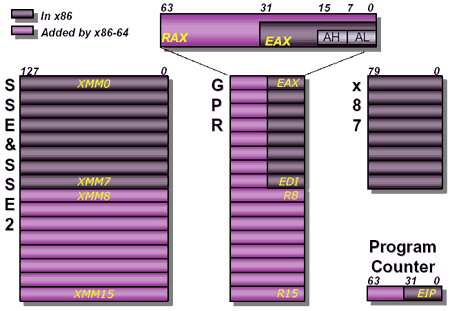
What makes Hammer special extends far beyond its ISA but we will first focus on that. AMD is hardly in a position to introduce drastic departures from the x86 ISA so the move to x86-64, an extension of the current 32-bit x86 ISA makes a lot of sense. And just because AMD isn't killing off x86 doesn't mean that Hammer is doomed.
We'll limit discussion on x86-64 but here are the main advantages:
1) backwards compatible with current x86 code
2) 8 new 64-bit general purpose registers (GPRs) as well as 64-bit versions of the original 8 x86 GPRs
3) SSE & SSE2 support along with 8 new SSE2 registers
4) Increased memory addressability for large dataset applications
5) Solid performance in current 32-bit applications with support for 64-bit applications going forward, a good transitional processor
With that said here are the basic cons:
1) continues to build off of the x86 ISA which many will agree, needs to go the way of the dodo
2) the new GPRs are only usable under 64-bit mode, making any increases in 32-bit performance outside of the ISA enhancements
There are many discussions on x86-64 alone, including our article from not too long ago but the focus of this piece is much more on the architecture behind Hammer rather than AMD's choice of an instruction set. So without further ado, let's learn how to make an already fast processor even better.
More than one way to skin a cat
It's easy to assume that AMD's next-generation CPU has to follow the same basic principles as Intel's NetBurst architecture:
1) very deep pipelining (20+ stages) to attain very high clock speeds (10GHz+ by 2006)
2) small, low latency caches and a very high bandwidth memory subsystem (e.g. RDRAM)
However it would make little sense for AMD to completely depart from their K7 architecture in order to make their future CPUs more P4-like. At the same time, AMD doesn't necessarily want to deal with the issues of extremely high clocked processors. As we talked about in our recent article on Intel's BBUL technology, as CPU clock speeds increase the packaging (what connects the silicon to the "outside world") becomes increasingly more important. Having just recently switched to non-ceramic packaging, a move Intel made in the late days of the original Pentium processor, it is unlikely that AMD would be able to develop the technology necessary to allow for their own 10 - 20GHz processors in the immediate future. Even Intel's Bumpless Buildup Layer packaging is a few years away and their packaging R&D teams significantly dwarf those at AMD. The bottom line is that from an engineering perspective, AMD can't go down the route of extremely high clock speeds as there are many areas outside of a CPU core that govern how high of a clock speed you can attain. What AMD lacks is the additional infrastructure necessary to follow the path of the Pentium 4.
This isn't necessarily a bad thing; look at some of the most powerful processors on the market today. In SPEC CFP2000 the Alpha 21264A running at 667MHz can outperform our beloved AMD Athlon at over 2x the clock speed, not to mention that Intel's own Itanium only runs at 800MHz while providing even higher scores. There is this clearly incorrect but popular feeling that when Intel designed the Pentium 4, a bunch of marketing gurus decided to create a processor that would only run at enormously high clock speeds. Intel understands just as much as AMD and the rest of the microprocessor manufacturers out there that there is more to performance game than just clock speed. AMD chooses to hype the number of instructions they can process in a single clock (IPC) since that's what their current processors excel at while Intel chooses to hype the clock speed they can attain for obvious reasons. Both IPC and clock speed are a part of the performance equation, meaning that you could theoretically design a processor to sustain a high IPC or a high clock speed.
Like the K7 architecture, AMD's Hammer is not designed around extremely high clock speeds but rather increasing IPC with a moderate boost in clock speed as well. This is far from the approach that Intel is taking with NetBurst and the Pentium 4 which doesn't make it right or wrong, just different.
She's got a nice pipeline
With the introduction of the Pentium 4 it became fashionable to talk about how many stages are in a processor's pipeline and the idea of a longer pipeline ended up getting a negative connotation in the eyes of many. Because the Hammer design is such a sharp contrast with Intel's NetBurst architecture that powers the Pentium 4 we thought it best to start out with where the two paths begin to separate the most: with their pipelines.
|
AMD
Integer Pipeline Comparison
|
||
|
Clock
Cycle
|
K7
Architecture
|
Hammer
Architecture
|
| 1 |
Fetch
|
Fetch
1
|
| 2 |
Scan
|
Fetch
2
|
| 3 |
Align
1
|
Pick
|
| 4 |
Align
2
|
Decode
1
|
| 5 |
EDEC
|
Decode
2
|
| 6 |
IDEQ/Rename
|
Pack
|
| 7 |
Schedule
|
Pack/Decode
|
| 8 |
AGU/ALU
|
Dispatch
|
| 9 |
L1
Address Generation
|
Schedule
|
| 10 |
Data
Cache
|
AGU/ALU
|
| 11 |
Data
Cache 1
|
|
| 12 |
Data
Cache 2
|
|
What you're looking at in the above table is the basic integer pipeline for K7 based processors and upcoming Hammer based processors. The path a floating point instruction would take would be longer but for our purposes these integer pipelines will work just fine.
The first thing you'll notice is that the Hammer has 2 extra stages in its pipeline compared to the K7; this 20% increase is clearly to provide for higher clock speeds and to prove that we'll have to look at the nature of the stages themselves.
At the start of this overview we talked about how today's high performance x86 processors obtained their standings by working around the limitations of the x86 ISA. One of the most common practices employed today is to take conventional x86 instructions and decode them into smaller operations that can be executed much quicker. As we found out in our investigation of the Pentium 4, these decode stages are actually very complex and are very influential to the end performance of a processor.
Those that are intimately familiar with the K7 architecture know that some of its decoding stages can vary depending on the type of instruction being decoded, but to keep things as simple as possible we have purposefully omitted those alternate stages; they don't change the analysis any.
The first time the two architectures diverge is in the 2nd stage where the Hammer has a second Fetch stage. This second fetch stage can be considered to be a transit stage; its purpose is to move the instruction that is to be executed from the instruction cache to the decoders. Intel has stages similar to this fetch stage in NetBurst that allow for data to be moved across the chip; the sole purpose of these types of stages is to increase clock speed.
The pick stage readies the instruction(s) for the first decode stages; it is much like the align stage from the K7 in that it tries to send as many independent instructions to the execution units as possible. The Decode 1 & 2 stages don't actually decode the instructions into the smaller operations (AMD calls them Macro-Ops); instead, these two stages are used to gather information about the instructions but not yet decode them. This is much like the Early Decode (EDEC) stage on the K7 where the correct instruction path is chosen (direct or vector) before the actual decode. The only difference here is that this early decode phase takes two cycles on the Hammer which again, allows the CPU to ramp in clock speed.
The pack stage then takes the information from the previous two decode stages and readies the instruction to actually be decoded into macro-ops. Then the macro-ops are dispatched and scheduled before they enter the execution units, and finally it's off to the L1 cache which holds true for both architectures.
As you can see there is only a difference of two stages in the basic integer pipeline of the Hammer and the K7. The benefit of this is that the IPC of the Hammer is not tremendously reduced by the lengthening of the pipeline; remember that the Pentium 4's pipeline was increased by 100% over the P6 pipeline whereas here we're only talking about a 20% increase. At the same time it also lends itself to the point that going forward, AMD probably won't be able to come close to the clock speeds that NetBurst will allow in the next few years.
Going from 'somewhat different' to 'drastic change'
Extending the pipeline by 2 stages will give AMD some additional frequency headroom but at the start of this article we mentioned an increase in IPC, not in clock speed, that would carry the Hammer. But where does this increase in IPC come from?
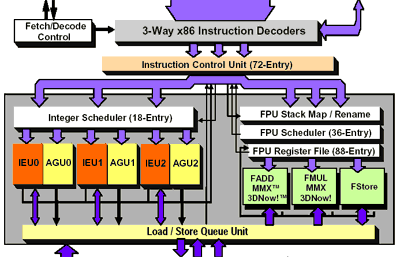
AMD's Athlon (K7) execution path
One way of increasing IPC would be to increase the number of execution units. The K7 architecture provided the Athlon with three Arithmetic & Logic Units (ALUs - these handle integer math), three Address Generation Units (AGUs - for loads/stores from/to cache) and three floating point units (FPUs - these handle floating point, or decimal math). AMD could have outfitted the Hammer with twice as many ALUs, AGUs and FPUs unfortunately they would not have seen a proportional increase in performance. Keeping the Athlon's execution units busy is a very difficult task; in fact, it's a difficult task for most of today's processors, including the Pentium 4. This is one of the reasons why there is such a large performance benefit to be had by increasing FSB clock since your CPU's execution units can be fed even more data.
Intel's solution to starved execution units is their Hyper-Threading technology that allows a MP aware OS to treat a single Hyper-Threaded processor as two CPUs and send two threads to it simultaneously. The idea behind this is that in most situations, a CPU's execution units are far from being fully utilized and by sending twice as many threads to the CPU you will be making more efficient use of those execution units. Intel expects to see a 10 - 20% increase in performance on regular applications courtesy of Hyper-Threading which is quite believable.
Like Intel, AMD realizes that throwing more execution units at the problem isn't going to solve this issue of increasing performance. Theoretically it may but in the real world things just don't work that way.
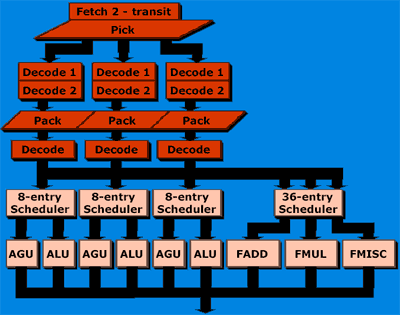
The Hammer's Execution Units are no different than the Athlon's
In an interesting but definitely not poorly chosen move, AMD has decided to stick with the K7's 3 ALUs, AGUs and FPUs. Although this may seem far from technical, the justification honestly comes down to "if it ain't broke, don't fix it." We're sure that AMD has done much more extensive profiling on the usage of the Athlon's execution units than we have, but it's safe to assume that the Athlon has no problem of running out of hands to work with.
That's great but we're still back to square one, how does AMD plan to increase IPC on the Hammer?
The answer to that comes in three of the major enhancements over the K7 architecture:
1) integrated memory controller & North Bridge
2) vastly improved branch prediction unit, and
3) what AMD likes to call "large workload TLBs"
There are no cute names for these benefits of the Hammer architecture and we'd have it no other way, so now it's time to dig into what really makes the Hammer special.
Integrated Memory Controller & North Bridge
For years AMD has been branded as nothing more than another follower, always looking to Intel for direction. We already know the fate of the other followers from Cyrix to IDT, but if there was ever one design that clearly set AMD apart from the group that they are placed in it would have to be Hammer; and you're about to see why.
Now is as good a time as any to really stress the need for greater system memory bandwidth and reduced memory latency. Since AnandTech was started back in 1997 we've seen the transition from EDO to SDRAM, from PC66 to PC133, from SDR to DDR and even a few others such as VC and DRDRAM. We've also seen how DDR SDRAM alone can increase the performance of the Athlon processor by 20 - 30%. We've also seen how much latency can impact the usefulness of these high bandwidth memory solutions. Poor memory access latency is what crippled the original ALi MAGiK1 chipset which was out months before VIA could offer DDR for the Athlon. But if CPU manufacturers can design such powerful CPUs why is it that no one can design an efficient way to get data from memory to them?
Let's take a look at the path data must take in order to get from memory to the CPU. When the CPU executes a read from system memory the command is first sent over the FSB to the North Bridge of the chipset which then hands it off to its integrated memory controller. These initial steps alone house a number of potential bottlenecks. Although very rare (since FSBs and memory buses are usually kept somewhat in sync), it is possible for a lack of FSB bandwidth to slow down this part of the memory read. Much more likely are inefficiencies within the North Bridge and its memory controller which would add costly delays to the retrieval of data from memory.
Now that the memory controller has the read request (we're ignoring any buffers it has to propagate through, etc…) it is sent over the memory bus, to the memory and after a series of operations the data is found and sent back to the memory controller. The memory controller takes the data, hands it off to the FSB interface within the North Bridge and back to the CPU it goes.
There is very little you can do about the second half of this process since it deals almost entirely with the type of memory used and the operating frequency of the memory bus. What can be controlled however are the first and last few interactions which are governed by the chipset and the FSB.
We had been thinking of an intermediate L3 cache as a way of reducing latency and improving bandwidth utilization between the North Bridge and the CPU however AMD's thoughts were on integrating the memory controller into the CPU itself.
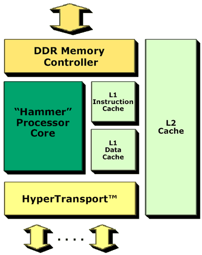
An overview of an AMD Hammer CPU
The benefits of a memory controller integrated into the CPU are tremendous; not only do you get much lower latency operation since all read/write requests no longer have to go through an external North Bridge before getting to memory but you also significantly reduce the chances of chipsets holding back the overall performance of a platform. We have seen countless examples of the Athlon being held back by platforms that are performing under par. At the same time, AMD has made it clear that they don't have the desire or the capability of becoming the chipset manufacturer that Intel is today. What better solution than to remove the problem altogether and integrate the memory controller into the CPU?
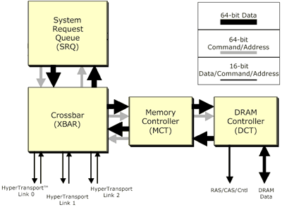
The Hammer CPU core interacts with the SRQ to send requests to the MCT/DCT through
a Crossbar controller. We have omitted some information from this diagram for
simplicity.
Thus the Hammer architecture calls for an integrated memory controller (MCT) and an integrated DRAM controller (DCT). The memory controller is a generic interface between the Hammer core itself and the DCT; this controller understands what memory is but isn't tied down to a particular type of memory. The MCT interfaces with the DCT which is much more specific and deals with specific types of memory. AMD could theoretically produce a Hammer with DDR SDRAM support and another with RDRAM support just by changing the DCT, but to end all speculation now, RDRAM would make very little sense on the Hammer. Remember that one of the downsides of RDRAM is increased latency in many situations; one way of hiding this latency is by pairing RDRAM with deeply pipelined CPUs such as the Pentium 4. It's obvious by now that the Hammer isn't as deeply pipelined of a CPU and won't have the clock speed to offset RDRAM latencies as well as the Pentium 4. This also makes AMD's decision to continue to support DDR SDRAM very sensible.
Integrated Memory Controller & North Bridge (continued)
The initial processors based on the Hammer architecture will feature either a 64-bit or 128-bit DDR SDRAM DCT. This DCT can support clock speeds of 100, 133 or 166MHz for DDR200, DDR266 or DDR333 SDRAM support. AMD has hinted very strongly that the replacement for a DDR based DCT would be a DDR-II based solution in later versions of Hammer based processors.
|
Memory
Bandwidth Comparison
|
||
|
Memory
Type
|
64-bit
DCT
|
128-bit
DCT
|
| DDR200 |
1.6GB/s
|
3.2GB/s
|
| DDR266 |
2.1GB/s
|
4.2GB/s
|
| DDR333 |
2.7GB/s
|
5.4GB/s
|
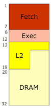 The
fact that the memory controller is on the CPU die itself also means that memory
accesses scale directly with clock speed since the data doesn't need to traverse
the FSB before getting to the CPU. The example AMD gave at MPF was of a theoretical
2GHz Hammer processor whose memory access latency was 12ns (see right for
Hammer pipeline). Obviously that's not taking into account the time it takes
to actually get data from memory, but it's much faster than going through
an external North Bridge before getting to main memory.
That's all great, but we still haven't answered the question of how AMD plans on improving IPC - actually, we have. By getting data from memory to the CPU much faster, the Hammer's execution units will be able to stay filled much better than the Athlon was able to which results in an increase in overall IPC.
And again, an integrated memory controller removes one of the major roles of the external North Bridge. AMD took this one step further and actually integrated a North Bridge on the CPU die as well. The only thing that remains of the conventional external North Bridge is an AGP controller. This should pretty much eliminate any major performance issues stemming from the chipsets that the Hammer is paired with; it will also make motherboard manufacturers happier since routing traces to/from the CPU and memory will be vastly simplified.
Below you'll see an example of what a single processor Hammer system would look like:
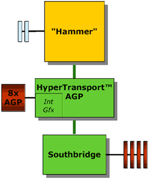
As you can tell from the picture, the AGP 8X controller is the only other chip that the chipset manufacturer has to provide outside of the South Bridge. The AGP 8X controller connects to the Hammer processor via a HyperTransport link. It is possible that a chipset manufacturer could produce a single chip that would house all of the functions of a conventional South Bridge along with the AGP 8X controller to provide for a very simple and cost effective Hammer motherboard layout.
Another thing to take away from this diagram is the fact that you only see two memory banks stemming off of the Hammer processor. AMD has indicated to us that single processor desktop Hammer systems will support a maximum of 2 unbuffered DIMMs.
Vastly Improved Branch Predictor
Don't be fooled; just because the Hammer's pipeline is only 12 stages long doesn't mean that AMD won't need an improved branch prediction unit to prevent the 20% longer pipeline from reducing IPC in situations where conditional branches are not easily predictable. Remember that a mispredicted branch in the Hammer faces a 20% longer penalty than the K7 making it very important for the Hammer to receive an improved branch prediction unit; and that it does.
You'll remember that one of the more elegant ways Intel had of dealing with branch mis-predict penalties is by the introduction of an execution Trace Cache. This cache stores instructions in their decoded form, in the order of execution so that a branch mis-predict won't result in another set of time consuming decoding steps. The trace cache actually works very well for the Pentium 4's target market: the single processor mainstream and performance desktop markets. However AMD is quick to point out that when it comes to what they call "large workloads," the trace cache isn't as efficient. AMD's definition of large workloads include programs with large datasets such as scientific calculations or a series of smaller programs that together act as a large workload for the processor. Examples of this would be a system running many concurrent operations such as a power user's desktop or workstation computer or even something like a SQL database server where many smaller transactions are taking place at once.
Before we go any further we have to see if there are indeed any merits to AMD's claims of inefficiencies of the trace cache when it comes to large workloads. In our original 760MP review we ran three different iterations of CSA Research's Office Bench 2001; each subsequent iteration had a significantly increased workload that was mainly governed by the number of processes being run. For example, the baseline performance tests had no background tasks running while the loading level 2 tests had multiple instances of windows media player and many concurrent DB accesses among other loading tools. All theoretical indications would put the Intel Xeon 1.7GHz processor on top of the Athlon MP 1.2GHz processor (both 1P systems) in terms of how well they can handle the additional load. The Xeon (like the Pentium 4), has much more FSB and memory bandwidth which will easily be stressed by this test.
With the second iteration of the test, the loading level was set to 1 or a medium application load. In comparison to the baseline test, both the Athlon MP 1.2 and the Xeon 1.7 were 39% slower with the newly added load. Cranking up the notch yet again however revealed that the Xeon was 3.1x slower than the unloaded Xeon while the Athlon MP was only 2.7x slower than its unloaded counterpart. It would be silly for us to assume that this discrepancy is due to the inability of the trace cache to perform well in heavily loaded scenarios but it does present a possible support for the argument.
Unlike the Pentium 4, AMD's Hammer must be a one size fits all solution to AMD's entire product line going forward. It will go up against the Itanium in 4 and 8 processor servers while at the same time a version will eventually be used in the mobile and entry-level desktop markets. AMD is first going to introduce Hammer to the high end workstation and server markets where the laws of large workloads apply and they make it a point to state that a trace cache isn't a solution for them.
Instead AMD has vastly improved the arguably crippled branch prediction unit of the Athlon in the Hammer. The branch target array has the same 2K entry limit and 12-entry return stack as the Athlon, but the unit itself has been improved tremendously. For starters, the Hammer has these branch selectors which are bits stored in the L1 cache that contain information about where branches in the code exist and what type of branches they are. These branch selectors also have an additional bit that can flag the branch as static thus allowing the processor to predict it statically. A static branch is one whose outcome is almost always known, such as a branch to error codes in a program and thus it makes little sense to do any guesswork in predicting whether that branch will be taken or not. This helps prevent the global history counter, a collection of the history of branches to aid in prediction, from becoming cluttered with unnecessary information since when the processor branched to a particular error code will not help predict any non-static branches in the code later on.
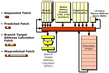
The final feature of the Hammer's branch prediction unit is a bit of logic called the Branch Target Address Calculator (BTAC). Before we explain this it's important to note what the Itanium does when faced with multiple conditional branches; the Itanium is a very powerful monster and has the power to evaluate various chunks of code simultaneously, including both conditions of a branch, and at the end of it all choose the "correct" data and discard what is useless instead of predicting where the branch will take the CPU. For example, let's assume that these instructions are sent to an Itanium optimized compiler:
…
3*4
Load Data from Memory Address A into Register 5
If Register 5 is negative then branch to Case 1, else branch to Case 2
Case 1:
12*6
Case 2:
1+1
…
The above snippet wasn't meant to be complex code at all but it can be used to show you how the Itanium would work. Intel's Itanium would execute both Case 1 and Case 2, determine the value in R5 and discard whichever case would not be used. The Hammer isn't engineered in an entirely different manner; while it won't even attempt to extract the level of parallelism in the code that the Itanium does, what it will do is attempt to better predict the outcome of branches. In this case, the Hammer would calculate the direction a branch appears to be taking and use its Branch Target Address Calculator to actually calculate the branch. This little distraction only eats up around 5 clock cycles and dramatically improves the efficiency of the processor's ability to predict branches by removing some of the guesswork and actually calculating the direction and path of a branch. As you might be able to guess, this is another source of increased IPC with the Hammer.
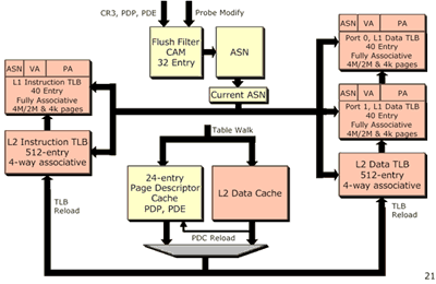
Large Workload TLBs
When AMD introduced their Palomino core one of the enhancements was an increase in the number of translation lookaside buffer entries (TLB entries); an increase in TLB entries reduces the amount of time wasted going to main memory for virtual to physical address translation. Even though memory latencies are significantly reduced with the Hammer's on-die memory controller, the increase in entries does shave off previous clock cycles for certain operations. It's unclear how big of a performance boost can be attributed to the increase in TLB entry sizes, but the increases are most likely reserved for very large workload scenarios (mainly in the workstation/server arenas).
An even more interesting aspect of the Hammer's TLBs is that they are managed very well during task switches. Normally whenever a processor switches tasks, for example when working on a new thread, the processor must flush the contents of the TLBs. In a multitasking environment however, where tasks are switched to and from continuously it can be a pain to refill the TLBs over and over again. Modern day RISC CPUs use a system of assigning a process id to keep track of the contents of TLBs allowing the TLBs to be flushed when switching process ids but quickly restored when switching back to the original process. The Hammer supposedly contains similar technology.
Hammer's Caches
We've spent this entire time discussing the architecture behind the Hammer line of processors but not much attention has been given to the usual metrics we compare processors by on a higher level. The cache subsystem of the Hammer hasn't changed too much from the Athlon; the 64KB L1 data cache is 2-way set associative (low latency and thus low hit rate) as is the 64KB L1 instruction cache, both unchanged from the Athlon/Athlon XP.
The L2 cache is once again variable in size, but this time around AMD is only committing to a maximum of 1MB for the L2 cache. This is particularly interesting because upon the release of the Athlon AMD was hinting at the possibility of L2 cache sizes up to 8MB. While we do know that 1MB Athlon's based on the nixed Mustang core were produced, nothing like that ever made it to market neither did anything with a larger L2 cache.
What will most likely happen is that we will see 512KB parts for the performance desktop and entry-level workstation segments, and 1MB parts for the high end servers. On a 0.13-micron process it shouldn't be too difficult to fit 512KB on the Hammer's die and it would be a sin to outfit the processor with anything smaller especially considering AMD's stressing of its stellar performance when dealing with large workloads. If AMD were to eventually create a Duron-like version of the Hammer then it would be feasible that a processor like that would only have a 256KB L2 cache.
Once again the L2 cache is 16-way set associative like the Thunderbird/Palomino cores however AMD assured us that the L2 cache was designed independently of the Athlon making any similarities between the two purely because that's the right way for them to do it. While AMD did confirm that internally the L2 cache would be dealt with more efficiently, we have yet to get confirmation that the L2-core interface has been widened from the currently crippling 64-bit data path.
Multiprocessing
Although the Hammer was designed as a top to bottom solution for the highest end servers down to the smallest notebooks, it's clear that the majority of its design choices were inspired by the workstation/server nature of the CPU. Case in point would be Hammer's multiprocessing capabilities.
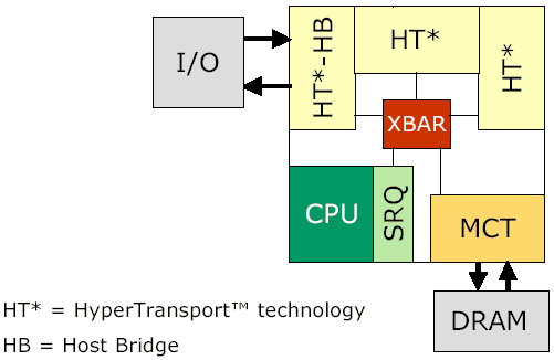
A Hammer with three Hyper Transport links
One of the biggest problems with designing and validating multiprocessor platforms is that the chipsets especially when dealing with a point to point bus protocol like the Athlon's EV6, are very difficult to design and implement on a board. The Hammer obviously doesn't use the EV6 bus (it uses AMD's own Hyper Transport) but it solves this issue of MP implementation by including up to two more Hyper Transport (HT) connects on each processor. You'll remember that one HT connect is used to interface with an external AGP 8X controller; the other two HT connects can be used to interface to up to two other processors.
Each processor has its own memory controller but to the OS and applications the memory is a unified array of memory. If a CPU is attempting to access memory controlled by another CPU, the read instruction is passed along from CPU to CPU until it finds the CPU with control of the memory and then it is sent to the CPU that requested it.
Each of the HT links and the memory controller are connected to a crossbar arbiter logic that handles the juggling of all of these requests coming from other CPUs and other logic outside of the CPU. Again the beauty of this is that the performance of the crossbar controller scales with clock speed meaning that the faster the CPU gets, the quicker the crossbar controller can move data between the various HT links and the memory controller. This is a welcome departure from the fixed frequency FSB in conventional systems that does not increase as CPU clock speed goes up.
|
The
Multiprocessing Capabilities of Hammer
|
||
This method of setting up MP systems without extraordinary requirements on the external chipsets has the potential of finally bringing 2P solutions down to the desktop level. While this may be a stretch, it does seem very plausible given the MP architecture of Hammer.
Final Words
This was a fun article to write because the architecture behind Hammer is truly very interesting. It's refreshing to see another approach to the problem of improving performance. The sharp contrast that the Hammer makes with Intel's NetBurst architecture that is behind the Pentium 4 doesn't make it better; it just means that AMD will have a different set of problems to face going forward.
We refrained from making any direct comparisons to other processors in this article other than on an architectural level simply because it's far too early to make any assumptions about the real world performance of Hammer or the processors it will be competing against. The two Hammer based processors we do know about that are codenamed SledgeHammer and ClawHammer (server and performance desktop respectively) should begin sampling in the second half of 2002. You can equate this sampling to the limited quantities of Athlons that were in the market towards the end of 1999, but hopefully we won't have to endure the same motherboard fiasco with the Hammer line. The real ramp of the Hammer architecture will occur in 2003 where the Athlon will begin to fade out of the picture.
AMD is clearly not the company it was a few years ago. They are constantly making steps towards becoming more of an industry leader as opposed to the follower they have been criticized of being for so long; the Hammer architecture is the most vivid depiction of what sort of an industry leader AMD is capable of being.
At the same time we shouldn't discount Intel as they still hold the majority of the market and they do have the potential to take their technology very far. What AMD's recent gains do prove however is that there won't be a return to domination for Intel anytime soon; this two man race will be continuing for some time to come. Both AMD and Intel have had their slipups; while Intel's have been more recently, AMD is far from immune to them.
The technology behind Hammer is there, as is the potential for it to succeed. But AMD has a lot of work to do between now and its release in the next 12 months. Many forget that until the Athlon, AMD didn't have the best execution track record. It's a long road ahead for the Hammer design team, good luck guys.

