Original Link: https://www.anandtech.com/show/8234/arms-mali-midgard-architecture-explored
ARM’s Mali Midgard Architecture Explored
by Ryan Smith on July 3, 2014 11:00 AM EST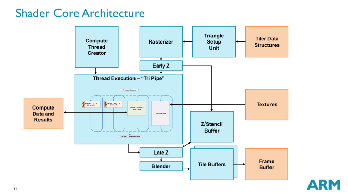
So far this is shaping up to be a banner year for SoCs. From a market perspective the mobile hardware space is still in a period of significant growth, but more importantly from a hardware point of view these products and especially the GPUs in these products have made significant strides in performance and in features. SoC GPUs will approach feature parity with desktop GPUs this year, and from a performance perspective they’re nearing the performance of the last-generation game consoles, a long-aspired goal given the “good enough” status attached to those devices.
Meanwhile at the same time that these products are maturing at a technical level, we’ve seen the various SoC firms mature at a professional level. The “wild west” days of SoCs have given way to mature markets of longer product cycles, longer product lives, and a more stable market overall. This both good and bad news for the various players in the SoC market as firms get squeezed out – SoC integrators such as TI and STMicroelectronics have been the first of such victims – but it also means that as companies become better established and more deeply entrenched, they can be more open about their projects and their products, and discuss them in greater detail than before without needing to be concerned about getting scooped by a competitor.
Here at AnandTech we’re particularly fond of doing architectural deep dives; our chance to talk to the people behind various processors and learn from them about how their products work and how they came together. Thanks to the maturation of the SoC market we’re finally getting a level of access in the SoC market that we haven’t had before, and in turn for the first time we get to tell the stories of the people behind these mind-bogglingly complex devices while better learning how they operate and as such how they compare. It’s admittedly a level of access we take for granted in the PC space, where companies such as Intel, AMD, and NVIDIA are regularly open, but it’s hard to contain our excitement about gaining this kind of access to the myriad of players in the SoC space.
This year then has been especially productive in that regard, and as of today it’s going to get even better. After we took a look at Imagination’s PowerVR Rogue architecture earlier this year, ARM contacted us and indicated that they would like to do the same; that they would like to take a seat at the “open architecture” table. To give us the access we need to discover how their GPUs work, and in turn tell you what we’ve learned.

To that end we’ve gladly let ARM pull up a seat, and today we’ll be taking our first in-depth look at ARM’s newest Mali SoC GPU architecture: Midgard. Now as with Imagination what we’re seeing today is most, but not all of the picture, as ARM has their secrets and they wish to keep some of them. But today we get to learn all about Midgard’s shader cores while also learning a thing or two about its pixel rendering pipeline, power optimizations, and other aspects of what makes Midgard tick. In other words, more than enough to keep us busy for one day.
But before we dive in we’d also like to quickly call attention to an Ask The Experts session we held with ARM’s Jem Davies, an ARM Fellow and VP of Technology in the Media Processing Division. While our deep dive is focusing on Midgard’s architecture, Jem has been answering all sorts of additional Mali-related questions, including business strategy and ARM’s views on GPU computing.
Finally, as this is the second article in our continuing series on SoC GPUs, we will be picking up from where we left off after our last article. While all of our articles are meant to be accessible to some degree, if you haven’t caught any of our previous articles I’d highly recommend our primer on how GPUs work for a quick overview of the technology before we dive into the nuts and bolts of ARM’s Midgard architecture.
A Brief History of Mali
ARM as a CPU designer of course needs no introduction. The vast majority of the world’s smartphones and tablets are powered either by an ARM designed CPU or a CPU based on ARM’s instruction sets. In the world of SoC CPUs, ARM is without a doubt the 800lb gorilla.
However in the world of SoC GPUs, while ARM is a major competitor they are just one of several. In fact from a technology perspective they’re among the newest, having roots that go back over a decade but still not as far as the rest of the major competitors. This is something of a point of pride for ARM’s GPU team, and as we’ll see, results in a GPU design that’s not quite like anything else we’ve seen so far.
Like all good GPU stories, the earliest history of ARM’s GPU division goes back to the late 1990s, where what would become ARM’s GPU division was first created. Originally a research project by Norwegian University of Science and Technology, the core Mali group was spun off to form Falanx Microsystems in 2001. At first Falanx was attempting to break into the PC video card market, a risky venture in the post-3dfx era that saw several other PC GPU manufacturers get shaken out – S3, Rendition, Revolution, and Imagination among them – and ultimately a venture that crashed and burnt as Falanx was unable to raise funding.
During a period of development of which they call their “scrappy phase,” due to their limited resources Falanx pivoted from designing PC GPUs to designing SoC-class GPUs and licensing those designs to SoC integrators, a much easier field to get in to. From this change in direction came the first Mali GPUs, and ultimately Falanx’s first customers. Among these were Zoran, who used the Mali-55 for their Approach 5C SoC, which in turn ended up in a couple of notable products including LG’s Viewty. But with that said, Falanx never saw great success on their own, never landing the “big fish” that they were hoping for.

LG's Viewty, One of Mali's First Wins
Ultimately as the SoC industry began to heat up from growing cell phone sales, ARM purchased Falanx in 2006. This gave ARM a capable (if previously underutilized) GPU division to create GPUs to go along with their growing CPU business. And from a business perspective the two companies were a solid match for each other as Falanx was already in the business of licensing GPUs, so for Falanx this was largely a continuation of status quo. Though for what was becoming ARM’s GPU division this was just as much of net win as it was for ARM, since it gave the Mali team access to ARM’s engineering resources and validation, capabilities that were harder to come by as a struggling 3rd party GPU designer.
Now as a part of ARM, the Mali team released their first OpenGL ES 2.0 design in 2007, the Mali-200. Mali-200 and its immediate successors Mali-300, Mali-400, and Mali-450, were based on the team’s Utgard architecture. Utgard was a non-unified GPU (discrete pixel and vertex shaders) designed for SoC-class graphics, and over the years received various upgrades to improve performance and scalability, especially on Mali-400 where Mali products first introduced the ability to use multiple cores.
Even to this day Utgard is arguably the Mali team’s most successful GPU architecture, based in large part on the architecture’s no-frills ES 2.0 design and resulting low die space requirements. Along with driving high-end SoCs of the era, including those that have powered devices such as the Samsung Galaxy S II, Utgard remains a popular mid-range GPU to this day, with Mali-450 securing a spot just this week in Samsung’s forthcoming Galaxy S5 Mini.

Mali-450 Lives On In Samsung's Galaxy S5 Mini
Now with a team of nearly 500 people and having shipped 400 million Mali GPUs in 2013 (or as close to “shipping” as an IP licenser can get), the Mali team’s latest architecture and the subject of today’s article is Midgard. Midgard ships as the basis of ARM’s Mali-T600 and Mali-T700 family GPUs, and while it was initially introduced as a high-end architecture, it will be making a transition to cover both the high-end and mid-range through the recent introduction of more space/power/cost optimized designs. After initially replacing Utgard at the high-end last year, this year will see Utgard finally replaced in the mid-range market.
Midgard: The Modern Mali
As ARM’s current-generation SoC GPU architecture, at the highest level the Midgard architecture is an interesting take on GPUs that in some ways looks a lot like other GPUs we’ve seen before, and in other ways (owing to its uncommon ancestry) is radically unlike other GPUs. This is coupled with the fact that as an SoC GPU supplier, ARM is in an interesting position where they can offer both CPU and GPU designs to 3rd party licensees, unlike most other GPU designers who either use their designs internally (Qualcomm, NVIDIA) or only license out GPUs and not ARM CPUs (Imagination). From a sales perspective this means ARM can offer the CPU and GPU designs together in a bundle, but perhaps more importantly it means they have the capability design the two in concert with each other, being in the position of the sole creator of the ARM ISA.
Architecturally Midgard is a direct descendant of Utgard. While there is a significant difference in how unified and discrete shaders operate, and as a result they cannot simply be swapped, the resulting shader design for Midgard still ends inheriting many of Utgard’s design elements, features, and quirks. At the same time the surrounding functionality blocks that compose the rest of the GPU have received their own upgrades over the years to improve performance and features, but are none the less distinctly descended from Utgard as well. At the end of the day this is a distinction more important for programmers than it is users (or even tech enthusiasts), but going forward it’s interesting to note just how similar Utgard and Midgard are, a similarity we don’t normally see between unified and discrete shader designs.

From a design standpoint Midgard is designed to span much of the range for SoC GPUs, from cheap, area-efficient designs to relatively massive designs with an eye on gaming. In doing so ARM offers a few different variations on the Midgard design that are all architecturally identical, but will vary slightly in features and internal organization. So for the purposes of today’s article we’ll be focusing on ARM’s latest and greatest design, Mali-T760, but we will also be calling out differences as necessary.
First and foremost then, let’s talk about design goals and features. Unlike the bare bones OpenGL ES 2.0 Utgard architecture, Midgard has been designed to be a more feature-rich architecture that not only offers solid graphics performance but solid compute performance too. This is in part a logical extension of what a unified shader GPU can already do – they’re innately good at mass math for graphics, so compute is only a minor stretch – but also a deliberate decision by ARM to push compute harder than they would otherwise have to for merely a graphics product.
From an API standpoint then Midgard was designed as what is best described as an OpenGL ES 3.0+ part. The architecture was designed from the start to offer functionality beyond what OpenGL ES 3.0 would offer, a decision that has since benefitted ARM by allowing Midgard parts to keep up with newer API standards. In fact ARM has just recently completed OpenGL ES 3.1 conformance testing, with their updated drivers passing Khronos’s required tests. As such all Midgard parts at a hardware level can support OpenGL ES 3.1, with software support reliant on OS and device vendors shipping updated OSes and drivers that enable 3.1 functionality.
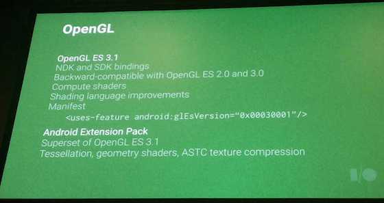
Even then Midgard has some functionality that has gone untapped, but will be enabled in the Android ecosystem through the upcoming Android Extension Pack for Android L. The AEP will further build off of OpenGL ES 3.1 by enabling features such as tessellation and geometry shaders, features that did not make it in to 3.1. As with OpenGL ES 3.1, ARM has confirmed that they expect all Midgard GPUs to support the AEP.
Finally, along with OpenGL ES support, ARM also officially offers Direct3D support on Midgard. This functionality has not yet been tapped – all Windows Phone and Windows RT devices so far have been Qualcomm or NVIDIA based – but in principle it is there. One thing to note however is that among the Mali 700 series, only Mali-T760 is Direct3D Feature Level 11_1 capable. Mali-T720 however only supports level 9_3, more befitting of the market realities and its status as a lower cost, lower complexity part.
Meanwhile from a compute standpoint Midgard is intended to be a strong competitor by supporting Android’s RenderScript framework and OpenCL 1.2 full profile. OpenCL support on SoC GPUs has been spotty due in part to the fact that the major OSes haven’t consistently supported it (iOS never has and Android only recently), and of those SoC GPUs that do support it, not all of them support the full profile as opposed to the much more restricted embedded profile. As is often the case with GPU computing just how well this functionality is used is up to the capabilities and imaginations of developers, but ARM has made it clear that they’re fully backing GPU computing even in the SoC space.
The Midgard Architecture
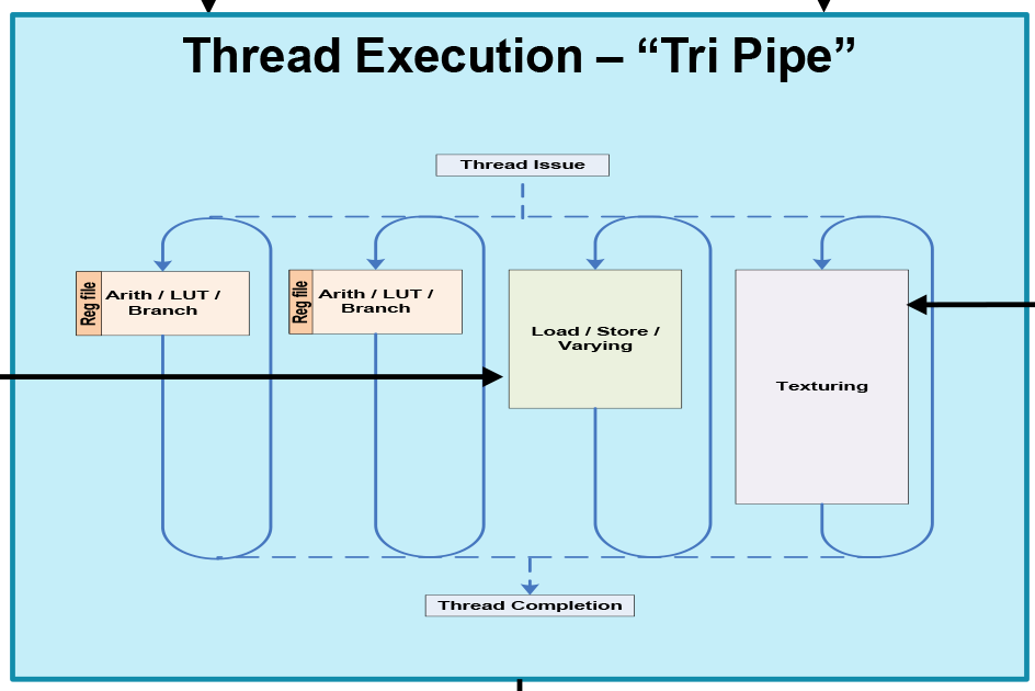
Diving in to the Mali architecture, we’ll start with a high level overview of the architecture. What we’re looking at here is a single Midgard shader core, which despite the “shader” name actually contains a whole lot more. A shader core in this context contains the actual shader core within one of Midgard’s “tri pipe” shader blocks, but also contains a triangle setup unit, rasterizer, Z & stencil hardware, a ROP/blender, tiling hardware, and a compute thread creator specifically for feeding a tri pipe with compute workloads.

Midgard – and Mali-T760 in particular in our case – is designed to scale up and down in performance and size on the basis of these shader cores. While they contain a large part of the hardware for a GPU, they are not on their own a complete GPU. They are instead designed to be laid down in multiples, and then fed by a collection of supporting hardware to make a complete GPU. This combination of shared hardware and scalable core counts allowing Midgard designs to scale from single cores up to a huge 16 cores in the largest Mali-T760MP16 configuration.
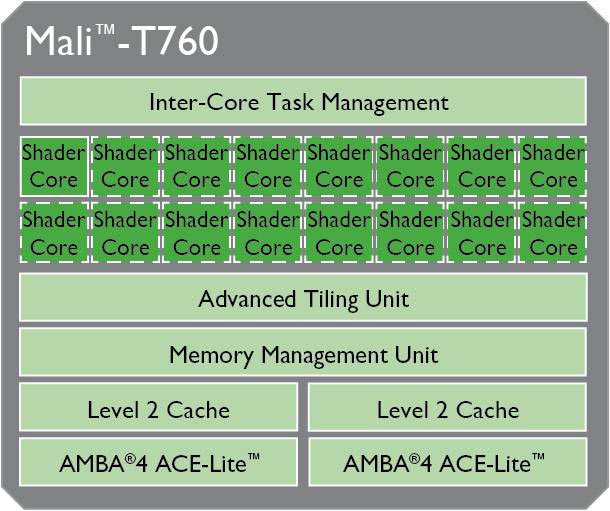
The shared hardware in Midgard is primarily concerned with managing the interaction of the shader cores, followed by providing the L2 cache and all further memory interfaces for accessing main memory and/or the CPU cache. In the case of Mali-T760 there is 1 task management unit and memory management unit, but 2 sets of L2 cache and the AMBA interface that connects the GPU to the rest of the system.
Jumping back to the core itself, let’s talk about the tri pipe for a bit. We’ll discuss arithmetic and thread execution on the next page, but from a high level a tri pipe is composed of one or more ALU blocks, a load/store unit, and a texture unit. From a high level the inclusion of ALUs, load/stores, and texturing in a single block is fairly typical for a GPU. However the variable number of ALU blocks is uncommon for a GPU. Many GPU designs maintain the same structure throughout and replicate what amounts to the tri pipe, rather than varying the number of units in the tri pipe itself.

As we’ve stated before, for our purposes we’re primarily looking at the Mali-T760. On the T760 ARM uses 2 ALU blocks per tri pipe, which is the most common configuration that you will see for Midgard. However ARM also has Midgard designs that have 1 ALU block or 4 ALU blocks per tri pipe, which is one of the reasons why seemingly similarly GPUs such as T760, T720, and T678 can look so similar and yet behave so differently.
| ARM Mali Midgard Arithmetic Pipeline Count (Per Core) | |||
| T628 | 2 | ||
| T678 | 4 | ||
| T720 | 1 | ||
| T760 | 2 | ||
Without being fully exhaustive, among various Midgard designs T628 and T760 are 2 ALU designs, while T720 is a 1 ALU design, and T678 is a 4 ALU design.
As one would expect, the different number of arithmetic pipelines per tri pipe has a knock-on effect on performance in all aspects, due to the changing ratio between the number of arithmetic pipelines and the number of load/store units and texture units. T678, for example, would be fairly shader-heavy, whereas the 2 ALU designs strike a closer balance between shading and texturing. Among the various Midgard designs ARM has experimented with several configurations, and with the T700 series they have settled on 2 ALU designs for the high-end T760 and 1 ALU for the mid-range T720 (although ARM likes to point out that T720 has some further optimizations just for this 1 ALU configuration).
In any case, each arithmetic pipeline is independent, working on its own set of threads. This is unlike some superscalar architectures, where additional arithmetic pipelines would be used for the execution of further non-blocking instructions in a thread.
The texturing unit meanwhile fairly simple. Midgard can process 1 bilinear filtered texel per clock, or 1 trilinear filtered texel over 2 clocks (to account for the second mipmap access). Note that the number of texture units and the number of ROPs per shader core is identical in the case of our T760, so in any core configuration there is a 1:1 ratio between texels and pixels.
Meanwhile, on one final stop while we’re looking at the functional blocks of Midgard, let’s talk about what we don’t see: a tessellation block. As we discussed before Midgard will support tessellation – T760 even supports Direct3D FL 11_1 – but nowhere will you see a tessellation block in the Midgard architecture.
As it turns out this isn’t an oversight or purposeful omission on ARM’s part, but rather an intentional design choice for Midgard. Midgard is fully capable of tessellation, it just does so without a fixed function unit to handle the geometry creation process.

Overview: Fixed Function Tessellator
In lieu of that Midgard implements tessellation on its shader hardware. Not just the hull and domain shader stages, mind you (which are done on shader hardware anyhow), but the actual geometry generation takes place there too. This is without a doubt a highly unusual situation, as we have never seen a tessellation-capable GPU without a dedicated tessellation unit thus far, making Midgard the first (and so far only) GPU we know of with such a design.
In discussing this design decision, ARM has told us that at the end of the day this choice is based on balancing the use of limited die space with benefits of a dedicated tessellation unit, and just how well the rest of the GPU can consume tessellated polygons. As it turns out the Midgard shader engine can tessellate at a higher rate than the rest of the pipeline can consume the additional polygons, meaning that a dedicated tessellation unit in the case of Midgard would not improve tessellation performance since it would be bottlenecked by the rest of the pipeline just as well. Furthermore any die space that ARM did dedicate to a tessellation unit would be die space they couldn’t dedicate to something else, such as additional shader hardware.
Ultimately whether this was the right decision or not is only something ARM can know – only they would have the simulation data for hardware tessellation versus shader tessellation – but this single omission already makes Midgard a highly unusual (and not to mention unique) GPU architecture. But from an outsider’s perspective we are left wondering what the power cost of this decision is. There’s no reason to doubt ARM’s space/performance argument, but as traditional GPU logic goes, doing anything in flexible hardware is going to be more power intensive than a highly specialized fix function unit, which is why we have so many of them in SoC GPUs and desktop GPUs alike. Performance aside, is shader tessellation significantly more power intensive than a theoretical hardware tessellation Midgard GPU? And if so, what does that do for power bottlenecking?
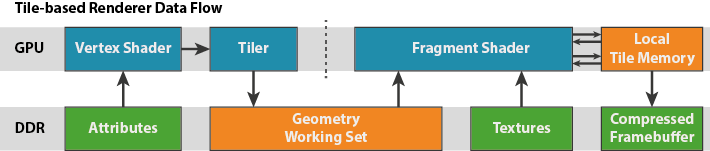
Moving on from our look at the fixed function units of the shader core to a broader execution picture, when it comes to graphics and like many other SoC-class GPUs, Midgard is a tile based architecture. This in a nutshell involves the GPU (specifically the tiler) breaking up scenes into individual tiles to be processed on a tile-by-tile basis, rather than rendering the scene at once, generally on a per-polygon basis. By breaking up a scene into tiles and then working on them one piece at a time, this allows Midgard to keep a constrained portion of the frame as the active workload, and in turn keep that tile in local memory on the GPU, rather than having to go to the slower main memory.
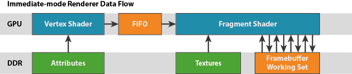
SoCs are ultimately constrained in every way possible – power, die size, and memory bandwidth – but it’s the last item more than anything else that can impact performance, making effective memory bandwidth usage especially important. Main memory accesses not only eat up valuable and limited memory bandwidth, but require burning further power to do so.
For Midgard ARM uses what they call a Hierarchical Tiling system, which as the name implies implements tiles on a hierarchical basis. The use of a hierarchy in this case allows Midgard to use variable tile sizes, based on the idea of further decomposing tiles (going down the hierarchy) until the tile complexity is at the desired size (or they’ve reached the minimum tile complexity). This ultimately allows Midgard to only use small tiles where it’s necessary, and conserve resources by working on large tiles where there is little scene complexity.

Making the best use of tiling does require some cooperation on the part of OSes and programs – Windows actually has a driver flag to indicate whether a GPU is a tiling GPU – but it offers some very important and necessary memory bandwidth optimizations for SoC-class GPUs. Making use of tiling just ultimately requires managing scene complexity to keep the tiling system and the memory footprint of the tiles under control, which is another situation of where Hierarchical Tiling flexes its muscles.
On the subject of tiling and bandwidth efficiency, Midgard also further cuts down on work and bandwidth wastage by rejecting work as early and as frequently as it can. The Early Z unit in each shader core can identify some polygons that would otherwise be covered and not visible, ejecting them before they make it to shading and texturing. And when that’s still not enough, Midgard (as of T620 and later) implements a technique called Forward Pixel Kill to further reject pixels. Forward Pixel Kill is at a basic level to pixels what Early Z is to polygons, identifying and rejecting covered pixels early enough to keep them from rendering. By keeping a small FIFO buffer and watching what pixels are being colored, Midgard can reject threads of pixels in mid-flight if it determines that the location they’re to be drawn is now covered by an opaque pixel.

Moving on, let’s talk about an area where ARM’s CPU background has come into play for their GPU designs: bitness and memory access. Developed alongside Midgard was ARM’s ARMv8 (aka ARM64) architecture. As one of the biggest design goals of ARMv8 was to extend it to a 64bit architecture, so the same choice was made for Midgard. As a result Midgard is fully 64bit; it can process 64bit Integers, double precision floating point numbers (FP64), and even natively use 64bit memory addresses. ARM wanted Midgard to be just as 64bit ready as ARMv8 would be.
The presence of 64bit operations is in and of itself fairly rare for an SoC GPU – 64bit operations are important for certain classes of compute workloads, but are seldom-to-never used for graphics operations – however ARM’s plans extend beyond just computational precision. Because Midgard can use 64bit memory addresses, Midgard can use the same 64bit address space as ARMv8 CPUs. This ability allows Midgard to achieve I/O concurrency with ARMv8 CPUs, allowing it to read directly from the CPU’s cache. Even with this Midgard and ARMv8 are not fully cache coherent – this feature is mostly about letting the GPU gorge on the CPU cache to more efficiently pass data from the CPU to GPU – but full cache coherency is coming.
In fact for as important as ARM’s decisions have been in making Midgard’s shader cores compute capable, equally as important is 64bit addressing and I/O coherency. ARM is after all a member of the Heterogeneous System Architecture (HSA) group, and has for some time now reiterated their intentions to back and invest in GPU computing both on a stand-alone basis and on a tightly integrated CPU/GPU basis. Midgard to that end is still in the stand-alone compute stage, but it incorporates optimizations that help performance right now while setting a clear roadmap towards an HSA-capable ARM CPU + GPU design. At the end of the day ARM needs to save power, and letting the GPU work on hardware-appropriate workloads is one such way to achieve this.
Finally, speaking of power let’s talk about Midgard’s power management capabilities. It would be disingenuous to merely state that Midgard is power optimized, as it implies that SoC GPUs are somehow not power optimized when in fact everyone is just as badly power bound, but going forward power consumption is only going to get more and more important as energy efficiency improvements from new fab nodes is not what it once was.
All told then, Midgard implements a number of tricks to reduce power consumption. Every rendering optimization we’ve talked about thus far is a power optimization, but on top of that Midgard implements both clock gating and finely grained power gating to either shut off power usage (or at least reduce it) for every inactive block as the situation allows. Each shader core sits on its own power domain, allowing cores to be shut down in the case of light workloads.
Even within those shader cores, the various blocks can be clock gated to bring down their power consumption. Inside the Midgard arithmetic unit the scalar and vector units can be separately clock gated, right down to the individual SIMD lanes of the vector unit itself.
Ultimately there’s only so much ARM can do to reduce power usage when a block is needed. In those cases ARM relies on achieving a balance between (relatively power hungry) clockspeeds and wide GPUs, and further utilizing workload rejection technologies to do what they can (and we’ll look at a couple more of those in a moment). But in lieu of the ability to further reduce power consumption under load, ARM is giving Midgard’s blocks a chance to rest whenever they can.
Midgard’s Arithmetic Pipelines
Having taken a look at Midgard’s architecture from a high level perspective, we next want to dive deep into the heart of Midgard: its arithmetic pipelines. This is where the bulk of the work takes place on any modern GPU, and in most cases real-world GPU performance significantly hinges on the design decisions made here. Furthermore this is where Midgard’s most unconventional design decisions lie, and as a result it’s the arithmetic pipelines that make Midgard stand apart from anything else we’ve seen.
ARM describes Midgard as a Very Long Instruction Word (VLIW) design with Single Instruction Multiple Data (SIMD) characteristics (though officially it is called Sequential Long Instruction Word). What this means is that at a high level ARM is feeding multiple ALUs, including SIMD units, with a single long word of instructions. But perhaps it’s better we start at a low level instead.
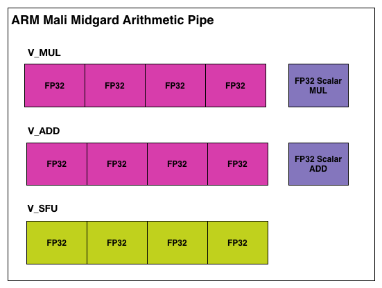
The above is a single Midgard arithmetic pipeline, in our example configured for FP32 operations. In it ARM uses a mix of both scalar and vector (SIMD) ALUs. Altogether ARM breaks it down as 3 vector ALUs and 2 scalar ALUs, each responsible for a specific type of operation.
If we stop for a moment and look at the SIMD, we find out something very interesting about it as well. Remember earlier how we mentioned that Midgard is capable of 64bit operations? Well this is how they do it. Not with separate 64bit and 32bit units as in some other designs, but by using a single 128bit wide SIMD and decomposing operations based on their width. The 128bit SIMDs in a Midgard core can process 2 64 bit operations, 4 32bit operations, or even 8 16bit operations per clock cycle. Simply fill the SIMD with as many (identical) operations as will fit, and the SIMD will handle the rest.
The use of SIMDs and SIMD-like designs is not uncommon in GPUs, but it’s relatively rare to see a flexible SIMD of this nature. In the past other architecture designers have talked about this being a efficiency tradeoff – you lose some efficiency by using a flexible design rather than a rigid design – however in ARM’s case they have decided that they can meet all of their goals with a 128bit SIMD.
Jumping back up a level, from a hardware perspective a Midgard arithmetic pipeline is capable of up to 17 FP32 FLOPS. This is constructed as the following.
- 4 vector adds
- 4 vector multiplies
- 1 scalar add
- 1 scalar multiple
- 1 FDOT4 dot product (7 FLOPS)
The vector and scalar operations are relatively self-explanatory, while the dot products are a result of using the vector special functions unit. To that end every architecture possesses SFUs in some form to handle dot products, transcendentals, and other complex operations, but their inclusion in FLOPS counting is uncommon. Most architectures merely count FLOPS as adds and multiplies through the ubiquitous and all important MAD (Multiply-Add) instruction. NVIDIA’s forthcoming K1 (to pick a GPU with a desktop counterpart) has 192 FP32 ALUs, and via MADs can achieve up to 384 FLOPS per cycle.
Ultimately how ARM counts FLOPS is entirely up to them, but we do want to take a moment to rectify it with how we count FLOPS on our end. Dot products are a relatively common mathematical operation in rendering, enough so that it’s important to be able to do them quickly, but they are generally not counted for computing FLOPS.
Meanwhile for FP64 FLOPS, as one would expect Midgard’s performance is much lower. ARM does not provide the FLOPS breakdown for 64bit operations, but they tell us that it is a total of 5 FLOPS. Our best guess here is that 4 of those FLOPS are coming from the vector units (2 FP64 MADs) and then 1 more FP64 FLOP is coming off of the scalar units, which if our assumption is correct would imply that it is not capable of an FP64 MAD in 1 cycle. Overall on a MAD basis this puts FP64 performance at 5/10ths, or ½ FP32 performance, which is a very high FP64 performance ratio even compared to desktop GPU architectures.
Furthermore, in further rectifying how ARM presents some of its data with how we typically present data in our articles, we’re also going to be using a condensed version of the Midgard arithmetic pipeline from this point on. As most architectures either utilize ALUs that can perform a MAD on their own or simplify their descriptions to showcase 1 ALU (rather than explicitly over 2 ALUs as on Midgard), we will be using a condensed version of the Midgard arithmetic pipeline that is drawn in a similar manner. Since we always count a standard ALU as being capable of 2 FLOPs (SFUs withstanding), this makes our Midgard arithmetic pipeline illustration consistent with our previous illustrations. It’s for all intents and purposes the same pipeline, only condensed.
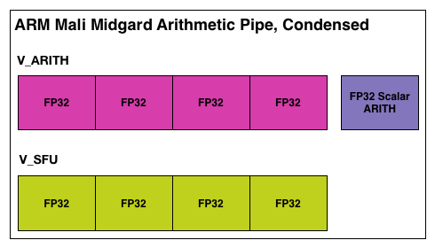
Finally, let’s take a quick look at a complete Midgard “tri pipe” core from an ALU standpoint. Since in T760 each core has 2 arithmetic units, a single core a just 2 of our condensed units. For a complete GPU this would then be multiplied by as many cores as the resulting design called for.
Midgard’s Execution Model: ILP, not TLP
Having seen the makeup of a Midgard arithmetic unit, we can finally get to the subject of thread execution on Midgard, and in the process get to what’s easily the least traditional aspect of the Midgard GPU.
As we mentioned before, Midgard is based on the idea of using VLIW with SIMDs, or as ARM likes to call it Sequential Long Instruction Word. In this execution model the Midgard shader compiler attempts to construct a single word of instructions in order to fill as many of the ALUs in an arithmetic pipeline as is possible. As is common for VLIW designs, this requires extracting a degree of Instruction Level Parallelism from the instructions being fed to the shader compiler, both to find operations that can be placed together on the SIMD units and to find operations that can then fill any of the otherwise idle units in a Midgard arithmetic pipeline. There is no superscalar execution going on here, but to make full use of a Midgard arithmetic unit you need to be able to bundle several operations together into the single VLIW word.
Depending on who you ask, an ILP-centric design either makes a great deal of sense or is difficult to program for, depending of course on the specific quirks of an architecture. From a hardware perspective this is very simple because the compiler does all the work while the hardware itself is merely executing VLIW instructions as requested. The hardware is not doing any scheduling or hazard checking on its own, and only really needs to deal with a stall (when a memory operand isn’t available in time). This saves die space and this saves power, and because all of your instructions in an arithmetic unit are from the same thread then you can save even more space because you have a group of ALUs working on the same thread with its data elements adjacent to each other.
Of all of the SoC_class GPUs we’ve looked at that are currently paired with ARM processors – NVIDIA’s Kepler and Imagination’s Rogue – both are designs that rely at least in part on ILP. Both also happen to be superscalar (something that’s not the case for Midgard), but at a basic level Midgard is in good company with its ILP-centric design.
On the other hand we have seen one other company attempt a VLIW and ILP-centric design in recent history only to abandon it. AMD used a vaguely similar VLIW design for their Radeon HD 2000 through HD 6000 parts, only to abandon VLIW for a non-VLIW design in 2011. At the time they cited that compute workloads weren’t mapping well to their design, and even graphics workloads were increasingly becoming less optimal. AMD’s replacement architecture, Graphics Core Next, used no ILP and relied entirely on Thread Level Parallelism.
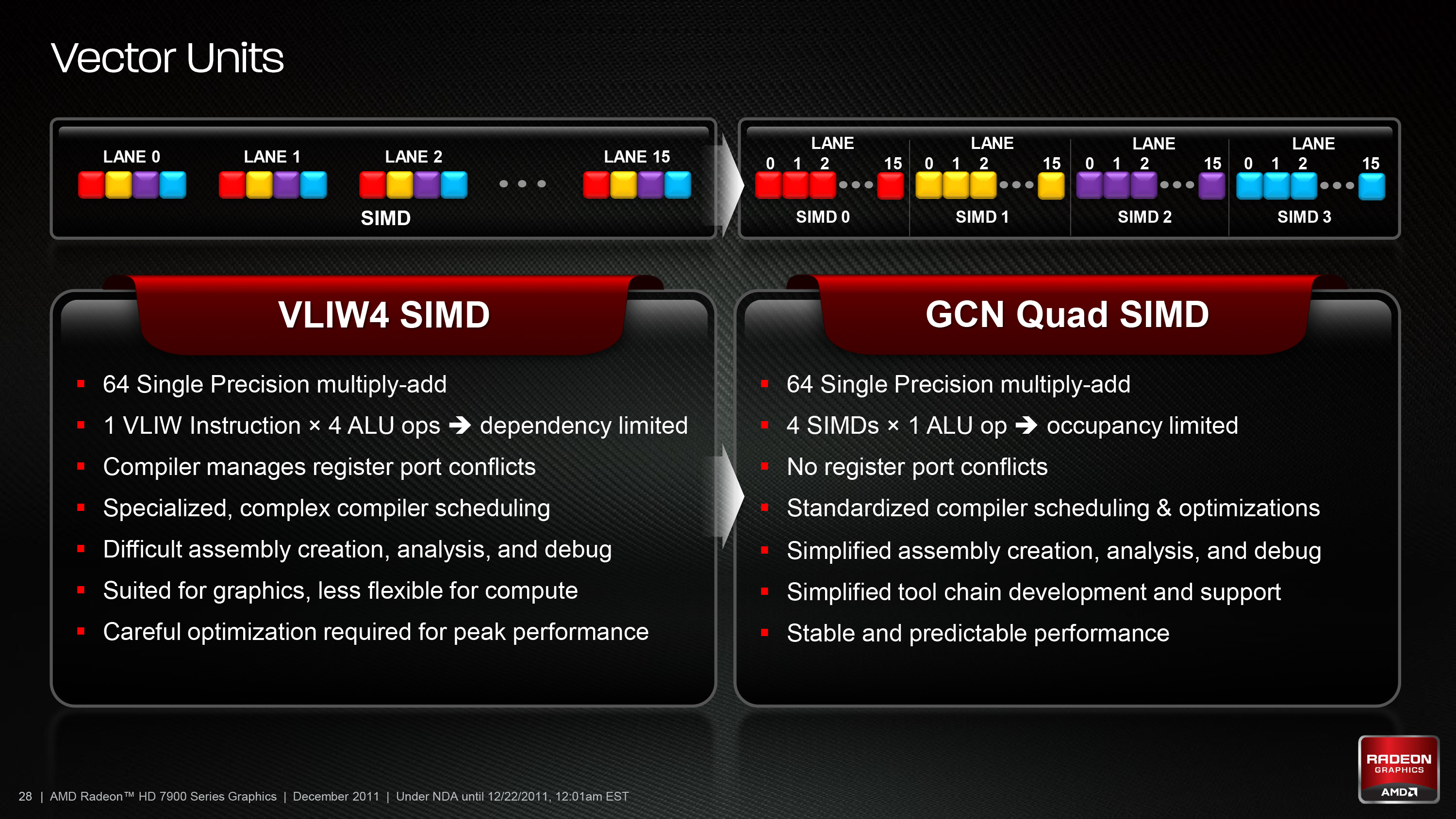
A Summary of AMD's Experiences With VLIW versus TLP SIMD
Ultimately the intended use case for Midgard is first and foremost graphics, and this is something that by all accounts it seems to do well at. For a simpler GPU design such as what would be suitable for an SoC-class GPU, VLIW is still a strong fit in ARM’s case because the 128bit vector SIMD maps well to RGBA shader operations (one color channel per SIMD lane) while the scalar unit covers anything else that doesn’t map well to the vector units. To that end we won’t spend too much more time covering the pros and cons of an ILP-centric VLIW design, but we did want to cover the history and how it compares to some other architectures.
Meanwhile, for anyone curious about the pipeline in an individual Midgard ALU, ARM also opened up to us on that front. In a very rare occasion in the GPU world ARM told us how deep their pipeline is, coming in at up to 128 stages deep for the entire Midgard pipeline. The artihmetic pipeline itself is under 30 stages deep but each pipeline of the tri-pipe design is a different length. Since we don’t know the depth of any other GPU pipelines we don’t have anything of substance to compare it to, but it is notable that ARM’s execution model is consistent with GPU execution models in general. A 128 stage deep pipeline invokes a high latency, high throughput machine that is interleaving a large number of threads to keep the pipeline full, which is in a nutshell an accurate description for GPUs in general. In any case, for Midgard ARM provides a further twist by bypassing misses (a failed attempt to read or write a piece of data) entirely; misses result in an instruction restart, rather than stalling the pipeline and all of the threads in it while waiting for the miss to be resolved.
Looking at the larger picture then, now that we how a single thread executes across one Midgard arithmetic unit let’s see how multiple arithmetic units work in concert. Or rather let’s not, because they don’t.
In the larger picture Midgard deviates from any other modern GPU we’ve seen in a very important way: Midgard does not extract thread level parallelism.
Every other GPU, be it Imagination, NVIDIA, AMD, or Intel, and whether it relies on ILP or not, also relies on thread level parallelism (TLP) to organize their work. In these designs multiple threads are bundled together and sent through an array of ALUs at once, where each thread in turn represents what is essentially a single pixel. Due to their spatial locality these pixels-as-threads are run together, the idea being that due to their locality they’re almost certainly going to have the same instruction applied, and in the end can be sent through ALUs that operate as a group and not independently. These wavefronts are a basic tenet of modern GPUs, whether it’s groups of 16 threads per cycle as is the case for AMD and Imagination, or groups of 32 threads per cycle as is the case for NVIDIA.
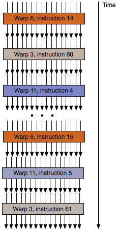
An Example of Wavefront/Warp Thread Execution On Other Architectures
But it’s this basic tenet that the Mali team has wanted to challenge, and in doing so they have put together an architecture in Midgard (and Utgard before it) that extracts no TLP from threads and executes each and every one of them independently. This, more than anything else, is the element that sets Midgard’s design apart from anything else we’ve seen so far.
As a result of this design decision, each arithmetic pipeline in Midgard is essentially its own CPU, consuming threads and processing them independently. Even in a single Mail-T760 tri pipe where there are 2 arithmetic units in a block these arithmetic units act on their own, working separately from one-another. Or to put this in to practice, in a large Midgard configuration such as T760MP16, this would mean a full 32 threads (16 cores * 2 math units) are being actively and independently executed.
Taken at face value then, this is a design that is very unorthodox and comes with a significant number of pitfalls that thread level parallelism is designed to compensate for. On the whole TLP is considered to be very easy to extract due to the spatial locality of pixels, which is all the more reason why on the desktop AMD went from a design that mixed ILP and TLP to a design that only utilized TLP. Furthermore because of the locality of pixels and threads, the ALUs in a design that does utilize TLP – typically a 16 or 32 wide array of SIMD ALUs – could be smaller due to the fact that they did not need the means to act independently, allowing more ALUs to be placed on such a GPU than would otherwise be possible.
But on the other hand TLP-centric designs do have their own drawbacks, and these are the reasons that ARM believes their non-TLP Midgard architecture is the way to go. First and foremost, TLP designs can only excel when threads/pixels need to flow together. If they need to go their separate ways, say due to a branching operation, then execution is slowed down to handle that branch. Alternatively, a group of threads that are branching may not be large enough to fill all 16/32 slots in a wavefront, in which case there are ALUs in the array executing the wavefront are going unused.

Midgard in contrast does not suffer from any thread related occupancy issues beyond very light workloads where even 32 threads (T760MP16) cannot be found, in which case Midgard gets to shut off whole cores. In fact because of this Midgard gets to branch for next to free due to the fact that there aren’t any other threads an arithmetic pipeline must concern itself with. Midgard arithmetic units can branch as they please and access memory as they please, an especially convenient scenario since tiling is already bounding the work area. At the same time however, this means that Midgard is going to be at its best in code with lots of branches, as otherwise in code with minimal branching will map well to traditional TLP-centric designs.
Meanwhile on the matter of tiling, this brings up another point ARM likes to make about Midgard versus TLP-centric designs, which is that they believe that wavefronts and tile based renderers are poorly matched. At times the limited number of threads/pixels in tiles would certainly exacerbate any issues keeping wavefronts filled with threads, among other things.
With that said from a theoretical perspective there’s not much more we can say on the matter other than to cover the execution model and the potential strengths and weaknesses of it. Other than that the proof is in the pudding, and that how well ARM’s unorthodox architecture performs is ultimately what determines if ARM has made the best move in creating such a unique architecture, or if there is a reason everyone else invests in thread level parallelism.
But for what it is worth, this design does go back to Utgard, and Utgard was (and continues to be) a solid performer for ARM. It has sold well over the years and would strongly suggest that a TLP insensitive architecture can in fact map well to workloads, at least for OpenGL ES 2.0 graphics.
Tricks of the Trade: Transaction Elimination and Frame Buffer Compression
While we have spent some time covering various techniques ARM uses to improve efficiency in Midgard, we wanted to spend a bit more time talking about two specific techniques in general that we find especially cool: transaction elimination and frame buffer compression.
Going back once again to what we said earlier about rendering and power efficiency, any rendering work ARM can eliminate before it’s completed not only improves performance by freeing up resources, but it also frees up power by not having to spend it on said redundant work. This is especially the case for anything that wants to hit system memory, as compared to the on-die caches and memories available to the GPU, system memory is slow and expensive to operate from a power perspective.
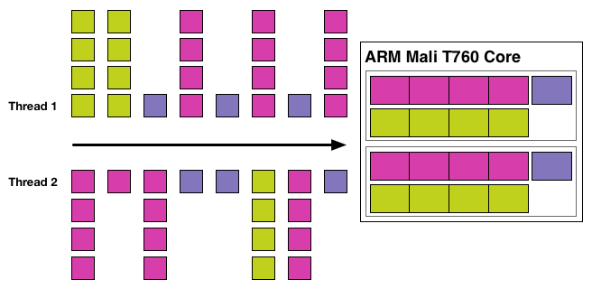
For their final two tricks then, having already eliminated as much rendering work as possible through other means, ARM’s last tricks involve minimizing the amount of data from rendered tiles and pixels that needs to hit system memory. The first of these tricks is Transaction Elimination (TE), which is based on the idea that if a scene (or parts of it) do not change, then it makes no sense to spend power and bandwidth rewriting those identical screen portions.
![]()
To accomplish this, ARM relies on their tiling system to break down the scene for them, and from there they can begin comparing tiles that are waiting for finalization (ROP/blending) to the tiles that are already in the frame buffer from the previous frame. Using a simple cyclic redundancy check to compare the tiles, if the tile to be rendered is found to be identical to the tile already there, the tile can be skipped and the memory bandwidth saved. Altogether of all of ARM’s various tricks, this is among the simplest conceptually.
The effectiveness of Transaction Elimination in turn depends on the content. A generally static workload such as a movie will have a high degree of redundancy overall (notably when the camera is not moving), while a game may have many moving elements but will still have redundant elements that can be skipped. As a result ARM can save anywhere between almost nothing and over 99% for a highly static workload, with the average more than offsetting the roughly 1.5% overhead from computing and comparing the CRCs.
Of course Transaction Elimination does have one drawback besides its low overhead, and that is CRC collisions. During a CRC collision a pair of tiles that are different will compute to the same CRC value, and as such Transaction Elimination will consider them identical and throw away the new tile. With a standard CRC value being 64bits, such a collision is rare but not impossible, and indeed will statistically occur sooner or later. In which case Transaction Elimination has no fallback method; it is judge, jury, and executioner as it were, and the new tile will be lost.
As a result Transaction Elimination is interestingly imprecise in a world of precision. When a collision occurs the displayed tile will be wrong, but only for as long as there is a collision, which in turn should only be for 1 frame, or 1/60th of a second.
Moving on, when worse comes to worse and ARM does need to write a new tile, on the Mali-T700 series GPUs they can turn to ARM Frame Buffer Compression (AFBC) to minimize the amount of memory bandwidth they spend on that operation. By using a lossless compression algorithm to write out and store a frame, memory bandwidth is saved on both the writing of the frame and in the reading of it.
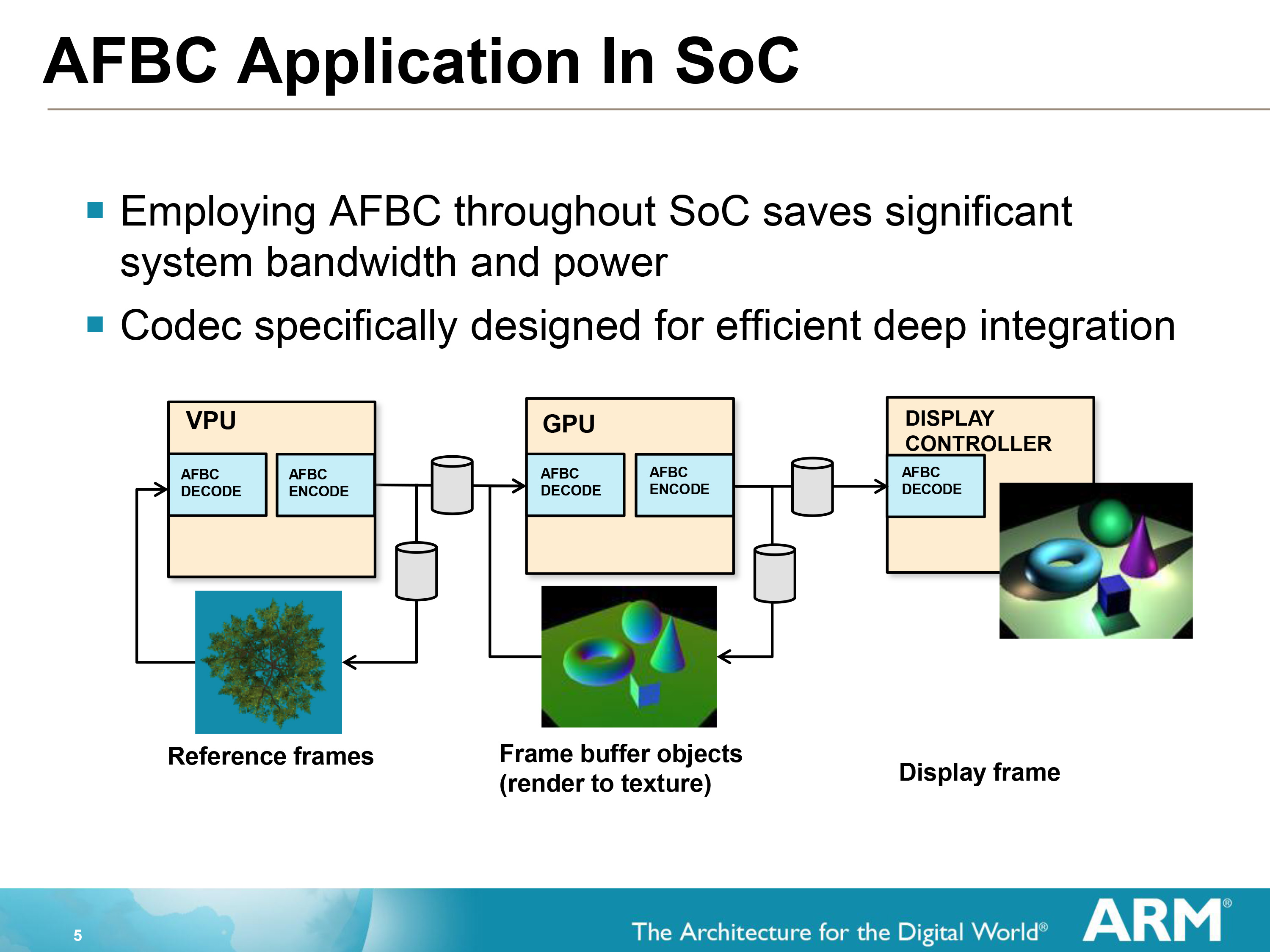
AFBC requires that both the GPU and the Display Controller support the technology, as the frame remains compressed the entire time until decompressed for display/consumption. Interestingly this means that the GPU needs to be able to compress as well as decompress, as it can reuse its own frames either in frame buffer objects (where a frame is rendered to a texture) or in Transaction Elimination. This becomes a secondary vector of saving bandwidth since it results in similar bandwidth savings for the frame even if the frame is never touched by the display controller itself. A similar principle applies to ARM’s video decoders (VPUs) which can use AFBC to compress a frame before shipping it off to the GPU.
On that note, it’s worth pointing out that while AFBC is an ARM technology, for interoperability purposes ARM does license it out to other display controller designers. ARM puts together their own display controllers, but because SoC integrators can use one of many display controllers it’s to ARM’s own benefit that everyone else be able to read AFBC as well as ARM can.
Technical Comparisons
As has quickly become tradition for us, to close out our look at the Midgard architecture we want to spend a bit of time comparing it to other SoC GPU architectures. As this is not a performance or benchmark article we aren’t going to dwell on the subject too much, but we find it’s helpful to get a high level overview of theoretical performance.
To do this we’ll take a quick look at theoretical performance for FP32 FLOPS, along with pixel and texel throughput. As this is a purely theoretical comparison it doesn’t (and can’t) take into account architectural efficiency, nor can it take into account real-world clockspeeds. But none the less it gives us something of a baseline.
To that end we asked ARM what a reasonable high-end Mali-T760 configuration might look like. T760 can scale up to 16 shader cores, but as we’ve seen in these scalable designs it’s very rare for anyone to build a SoC that actually takes the number of cores up to the architecture’s limit. And since T760 was only released to customers back in October of 2013, there are only a handful of designs announced so far and none of them are particularly high-end. To that end ARM suggested that a Mali-T760 MP10 would be a reasonable approximation of a high-end shipping configuration, so that is what we’ve gone with.
| GPU Specification Comparison | ||||||
| NVIDIA K1 | Imagination PVR GX6650 | ARM Mali-T760 MP10 | AMD A4-1350 | |||
| FP32 ALUs | 192 | 192 | 100 | 128 | ||
| FP32 FLOPs | 384 | 384 | 200 (340) | 256 | ||
| Pixels/Clock (ROPs) | 4 | 12 | 10 | 4 | ||
| Texels/Clock | 8 | 12 | 10 | 8 | ||
| GFLOPS @ 300MHz | 115.2 GFLOPS | 115.2 GFLOPS | 60 (102) GFLOPS | 76.8 GFLOPS | ||
| Architecture | Kepler | Rogue (6XT) | Midgard (T700) | GCN 1.1 | ||
Briefly, we can see that as far as theoretical shading performance is concerned, our theoretical Mali-T760 would push 60 GFLOPS when counting MADs (20 FLOPS/clock/core). Or when using ARM’s preferred metric of MAD plus a dot product (34 FLOPS/clock/core) this becomes 102 GLOPS. How you count ends up being important here as it means the theoretical throughput of the T760MP10 is either close to something like AMD’s A4-1350, or close to the very high end configurations that NVIDIA and Imagination will be peddling.
On the other hand T760MP10’s pixel and texel throughput looks very good, easily exceeding both our AMD and NVIDIA configurations on both and specifically more than doubling the pixel throughput. Pixel throughput is going to be especially important going forward as these SoCs get paired with increasingly high resolution displays – the TV industry has in recent years become big SoC consumers and 4K TVs are growing in popularity – so being able to push a lot of pixels will in turn be helpful for pushing such displays. However ARM’s efficiency technology such as Transaction Elimination and AFBC will also have to play a big part here, as writing that many pixels per clock raw would consume a large amount of memory bandwidth, something SoCs rarely have to spare.
Final Words
With apologies in advance to ARM, wrapping up this article the first thing that comes to mind is something we wrote when looking at Imagination’s Rogue architecture earlier this year: “So it’s with some hope and a bit of luck that this might get the ball rolling with the other SoC GPU vendors, getting them to open up their doors a bit more so that we can see what’s inside their designs.”
It’s safe to say then that we have indeed been lucky about getting other SoC GPU vendors to open up about their architectures. ARM’s decision to come take a seat at the “open architecture” table has given us a great opportunity to see into the heart of another SoC GPU and to better understand and appreciate just what’s going on under the hood when we look at Mali powered products. Plus in opening up on their GPU architecture, we have been given the chance to see what just may be the least conventional GPU of the modern era.
When ARM first began to brief me on the Midgard architecture, they told me that it would be something unlike anything else we’ve seen before, and while I believed them I don’t believe that description is quite strong enough to get across just how surprised I was by ARM’s autonomous, TLP insensitive shader design. It took the better part of a few days even after the briefing to really internalize just what they had done, and while it seems simple (and very cool) in retrospect, going for an unorthodox architecture certainly throws you for a loop at first after spending several years covering the world of wavefront-driven architectures.
As for Midgard and its resulting products, this stands to be an interesting and exciting time for ARM. The finalization of OpenGL ES 3.1 and the announcement of the Android Extension Pack means that some of the functionality that ARM has had to sit on thus far is finally going to be exposed and used. And meanwhile with 64bit Android coming up and ARM’s 64bit Cortex-A5x processors similarly near, ARM can begin exploiting some of that shared 64bit development that ARMv8 and Midgard went through.
At the same time however ARM also will face the same struggle for market share that the other SoC GPU vendors also face. As we’ve discussed in the past, the SoC GPU market is full of competitors, some who make their own SoCs and hence won’t be ARM GPU customers, and others who are in the licensing business just as much as ARM. With the latest generation Mali-T700 series parts ARM already has some T760 wins with MediaTek, who will be using T760 with their mid-range Cortex-A53 SoCs. But at the same time I’d love to see what flagship-caliber device would look like with a T760, so hopefully we’ll get that chance over the next year.
This incidentally is all the more reason to be open right now, as it’s that much easier to convince your immediate customers and even build a brand among end users when they can freely learn more about your products and how they operate. To that end the “open architecture” table remains open, and as we shift to the next generation of SoCs and next wave of SoC GPUs, with any luck this won’t be the last time we get to learn more about the GPUs that are increasingly in our everyday devices.


