Original Link: https://www.anandtech.com/show/8066/crucial-mx100-256gb-512gb-review
Crucial MX100 (256GB & 512GB) Review
by Kristian Vättö on June 2, 2014 3:00 PM EST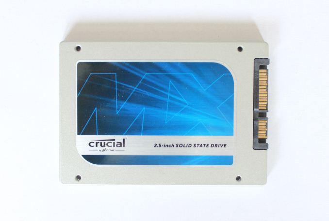
Computex is officially kicking off today and unlike many of the products announced at trade shows, we actually have a full review of the Crucial MX100 that is launching today at Computex. The MX100 is Crucial's new mainstream drive, replacing the popular M500 while the M550 will continue to serve the higher performance market. With the MX100 Crucial is aiming even lower in terms of price per gigabyte by utilizing Micron's (i.e. Crucial's parent company's) state-of-the-art 16nm 128Gbit MLC NAND. In fact the MX100 is the first mainstream product to use 16nm NAND and it's the smallest process node we have seen since Toshiba's/SanDisk's introduction of their A19nm NAND.
As we have discussed before, decreasing the lithography is the most effective way for NAND manufacturers to cut costs. The smaller lithography translates into smaller transistor size, which in turn means that the same amount of storage can be fit into a die that is physically smaller -- or you can fit more storage while keeping the die size the same. The smaller the die size, the more dies are received from each wafer, which reduces the production costs because you are basically getting more dies from the wafer without added cost. Well, almost.
For the past couple of years, every new lithography has reduced the profits and benefits that the die shrink brings. Sure the manufacturers still get more dies per wafer, but the investments required to research and manufacture the NAND have increased hand in hand with the die shrinks, making every die shrink less profitable than the previous. Furthermore, every die shrink introduces more endurance and reliability concerns because as you scale the cell, it becomes harder and harder to hold the electrons in the floating gate. That's why all major NAND manufacturers are researching 3D NAND as it will put an end (at least temporarily) to the scaling game since density can be increased by adding layers. I'll talk a bit more about the state of the NAND market and 3D NAND on the next page.
The MX100
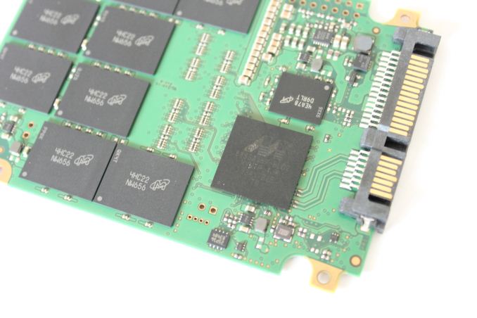
The short summary is that the MX100 builds on the same architecture as the M500 and M550. The only fundamental difference is the NAND inside as the controller is the same Marvell 88SS9189 silicon as found inside the M550. The 9189 is a minor upgrade over the 9187 and what it does is provide better support for DevSLP along with some bandwidth optimizations.
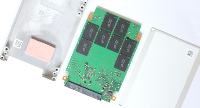
The design of the chassis and PCB remain unchanged as well, although the naming changes from Mxxx to MXxxx. I'm guessing Crucial had to change the naming because M600 would have been confusing given that the M550 will remain in the market as Crucial's high-end drive. Other than performance, Crucial is bringing some differentiation by offering limited capacities as the MX100 will only be available at up to 512GB, so those who want a larger drive will now have to pay for the M550.
| Crucial MX100 Specifications | |||
| Capacity | 128GB | 256GB | 512GB |
| Controller | Marvell 88SS9189 | ||
| NAND | Micron 16nm 128Gbit MLC | ||
| DRAM | |||
| Sequential Read | 550MB/s | 550MB/s | 550MB/s |
| Sequential Write | 150MB/s | 330MB/s | 500MB/s |
| 4KB Random Read | 80K IOPS | 85K IOPS | 90K IOPS |
| 4KB Random Write | 40K IOPS | 70K IOPS | 85K IOPS |
| Endurance | 72TB (~65GB/day for 3 years) | ||
| Encryption | AES 256-bit, TCG Opal 2.0 & IEEE-1667 | ||
| Warranty | Three years | ||
Due to the use of 128Gbit NAND, the write performance at smaller capacities takes a hit. I covered the reasons behind this in detail in the M550 review but in short the higher capacity per die means that fewer die are needed to achieve a certain capacity. This in turn reduces parallelism, which is the key of SSD performance in the first place. A single NAND die isn't very fast, but when you have multiple dies working in parallel, the performance adds up and you get hundreds of megabytes of throughput.
Feature wise the MX100 matches the M500 and M550. Both power loss protection and hardware encryption (including TCG Opal 2.0 and IEEE-1667 standards) are supported and the endurance rating remains at the same 72TB despite the change in NAND. Micron wouldn't give us the exact P/E cycle rating for their 16nm NAND but I was told that the endurance is similar to their 20nm MLC NAND. Even if there is a slight reduction in raw NAND endurance, it's possible to compensate for that by reducing the write amplification through firmware optimizations. RAIN (Redundant Array of Independent NAND) is also included to protect against page/block level failures and the parity ratio remains at 127:1 similar to the M550 (i.e. one bit of parity is generated for every 127 bits of user data).
IMFT's 16nm NAND
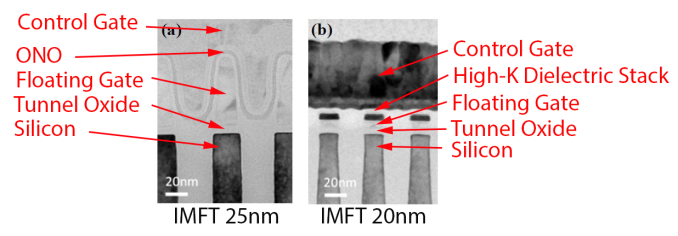
As I mentioned in the Plextor M6S & M6M review a couple of months ago, IMFT is doing something differently with their 20nm NAND. Let's see what it looks like:
That is what a cross-section of IMFT's 20nm NAND looks like in comparison to the 25nm node. There's quite a big difference. The 25nm node still used the traditional wrapping technology where the wordline (i.e. control gate) wrapped around every floating gate. However, the issue with this approach is its limited scalability. In addition to the wordline, the oxide-nitride-oxide layer (i.e. ONO) must be wrapped around every floating gate as well to insulate the floating gate because otherwise the electrons would be free to escape. And here lies the problem: the ONO layer cannot really be scaled any further without jeopardizing reliability because if it's too thin, it will not be able to reliably insulate the cell.
Furthermore, the reason why the wordline must be wrapped around each floating gate is to build enough capacitance between the control and floating gates as otherwise programming efficiency is lost. Remember that the way NAND works is basically fighting against the fundamental laws of physics because you are shooting electrons through an insulator, so the capacitance is crucial for quick and efficient programming.
If you can't scale the ONO layer, what do you do? Simply, you get rid of it and replace it with something better. The better in this case is a stack of high-K dielectrics. If you are familiar with Intel's CPU architectures, you may be familiar with the term as Intel introduced it to their CPUs with their 45nm process node. The high-K term refers to high dielectric constant, called K. The higher the constant K is, the higher the capacitance when the material is used as a dielectric. Obviously, high-K means that the constant is high, so the capacitance is also high.
All of the parts are now falling into place, right? Because the high-K dielectric stack has a much higher K value than the ONO layer, it's able to provide the same capacitance without the need for wrapping. As a result the technology is more scalable because the ONO wrap is no longer the obstacle.
IMFT introduced the high-K technology in their 20nm NAND and they are using the same technology in the brand new 16nm process. Unfortunately IMFT wouldn't disclose any details of their 16nm NAND (not even the die size) but this is most likely a symmetrical (i.e. 16nm*16nm) design as the use of high-K dielectrics allows scaling in both X and Y axes without major sacrifices in endurance or reliability. As a result the cell size is likely the smallest in the industry -- even though Toshiba's/SanDisk's NAND is officially called 15nm, they have not given any indication of the use of high-K dielectrics, which means the design is likely asymmetrical (e.g. 15nm*19nm) like their previous designs.
I'm guessing IMFT has a pretty significant lead in the high-K development given that Intel (the other half of IMFT) has been using them in their CPUs for years now. We'll find out more about the new NAND lithographies from every manufacturer as TechInsights and other companies specialized in semiconductor analysis are able to x-ray and analyze them.
The State of 3D NAND
If you've been following the SSD and NAND market for a while, it's likely that you have heard of 3D NAND. Scaling of standard NAND is starting to hit the laws of physics and it's getting tougher and tougher to shrink the cell size without driving into serious reliability and endurance issues. The cell size is simply getting so small that it can only hold a dozen or so electrons, which means that even a loss of one or two electrons through leakage/trapping can lead to a big enough change in the floating gate voltage that the cell becomes unreadable (i.e. it won't return the correct outcome).
This is where 3D NAND comes in. It puts a reset to the traditional planar scaling by stacking cells vertically. Now, just to be clear, this isn't the same as stacking several 2D NAND dies on top of each other, not at all. 3D NAND does the stacking at the wafer level, which leads to the actual die having multiple layers of cells (hence the 3D moniker). All NAND manufacturers are developing their own 3D NAND technologies and the approaches are all a bit different. Anand covered Samsung's technology in detail in our V-NAND announcement article but I'll save the analysis of the other manufacturers' technologies for a future article. Today we'll just look at the 3D NAND schedule for every manufacturer.
| IMFT | Samsung | Toshiba/SanDisk | SK Hynix |
| Q4'14 | Q3'13 | H1'16 | H2'14 |
Currently Samsung is the only company that has 3D NAND in mass production. Samsung has been producing their 128Gbit 24-layer 3D NAND in their Korean fabs since last August and just a few days ago they announced their second generation 3D NAND (or V-NAND as Samsung calls it). This is a 32-layer part with a die capacity of 86Gbit, so it looks like Samsung has cut the die size in half compared to their first gen V-NAND with the added layers providing the increase in density (64Gbit*1.33 is ~85Gbit). From what I have heard Samsung is using the same manufacturing equipment for their second gen V-NAND, so the odd capacity point makes sense because it's probably easier to optimize the controller for 86Gbit die instead of ~170Gbit, especially when dealing with low capacity drives/devices.
Furthermore, Samsung announced a while ago that their new facility in Xi'an, China has started the production of 3D NAND. The new fab isn't fully completed yet but Samsung expects it to be completed by the end of this year; regardless, it's clear that Samsung is leading the transition to 3D NAND. We will probably see 3D NAND make its first appearance in client-class SSDs this year because along with the second gen V-NAND announcement, Samsung also announced that they are already shipping 3D NAND SSDs to PC OEMs. However, I wouldn't totally rule out the possibility of yet another 2D NAND die shrink before Samsung moves to 3D NAND full time as from what I have heard, 3D NAND isn't currently very economical for Samsung and the price and characteristics make it more suitable for the enterprise market.
IMFT currently has samples of their 3D NAND but they are keeping everything in-house to make sure their competitors don't get their hands on them. Mass production is expected by the end of this year, although IMFT is making it clear that their 3D NAND won't replace 2D NAND anytime soon. Instead IMFT is developing a 256Gbit version of their 16nm NAND to remain price competitive and I've heard they are even working on a 10nm to 15nm process node. The usage of high-K gate dielectric certainly helps to scale traditional NAND even further but I guess it's ultimately up to how the 3D NAND production starts. If yields are good and the design is economical enough, there may not be a need for another 2D NAND die shrink, but we will probably hear more later this year.
SK Hynix is also planning mass production of their 3D NAND later this year. Similar to IMFT, SK Hynix believes that 2D and 3D NAND will co-exist for at least a couple of years until the challenges of manufacturing 3D NAND are solved. SK Hynix is currently entering mass production of their 16nm NAND, although it's not certain whether this is a symmetrical (16nm*16nm) design or whether it uses high-K dielectrics.
Last but not least, we have the Toshiba/SanDisk joint-venture. Their 3D NAND won't see mass production until early 2016, which is at least a year later than others. Toshiba and SanDisk believe that their 2D NAND is more cost efficient at the moment and thus see no need to move to 3D NAND yet. Their just announced 15nm NAND will be their last 2D NAND node but we probably won't see it in products until late this year or early next year, so that will cover the market for about a year before being replaced by 3D NAND.
All in all, the state of the NAND industry is certainly interesting. A lot will be happening in the next few years, though 3D NAND won't revolutionize the industry. (ReRAM and MRAM, on the other hand, may). I'm confident that 2D NAND will continue to be the go-to form of non-volatile memory for the mainstream market for the next two years or so and 3D NAND will be geared more towards enterprise, but we will see how things turn out.
And with that out of the way, let's move on to the performance testing of the Crucial MX100.
Performance Consistency
Performance consistency tells us a lot about the architecture of these SSDs and how they handle internal defragmentation. The reason we don’t have consistent IO latency with SSD is because inevitably all controllers have to do some amount of defragmentation or garbage collection in order to continue operating at high speeds. When and how an SSD decides to run its defrag or cleanup routines directly impacts the user experience as inconsistent performance results in application slowdowns.
To test IO consistency, we fill a secure erased SSD with sequential data to ensure that all user accessible LBAs have data associated with them. Next we kick off a 4KB random write workload across all LBAs at a queue depth of 32 using incompressible data. The test is run for just over half an hour and we record instantaneous IOPS every second.
We are also testing drives with added over-provisioning by limiting the LBA range. This gives us a look into the drive’s behavior with varying levels of empty space, which is frankly a more realistic approach for client workloads.
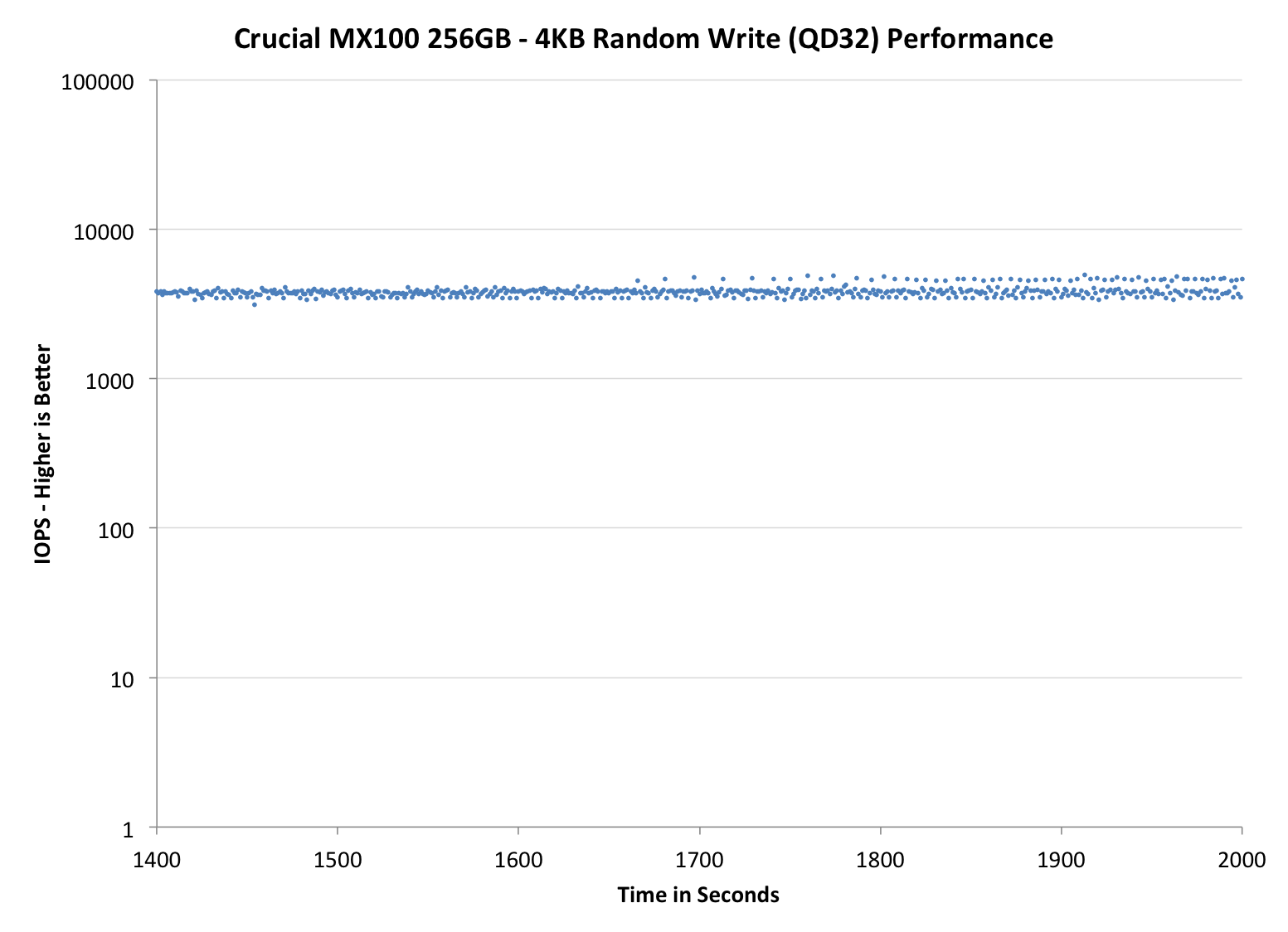
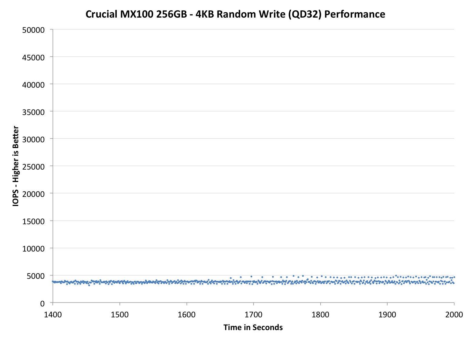
Each of the three graphs has its own purpose. The first one is of the whole duration of the test in log scale. The second and third one zoom into the beginning of steady-state operation (t=1400s) but on different scales: the second one uses log scale for easy comparison whereas the third one uses linear scale for better visualization of differences between drives. Click the buttons below each graph to switch the source data.
For more detailed description of the test and why performance consistency matters, read our original Intel SSD DC S3700 article.
 |
|||||||||
| Crucial MX100 | Crucial M550 | Crucial M500 | SanDisk Extreme II | Samsung SSD 840 EVO mSATA | |||||
| Default | |||||||||
| 25% Spare Area | |||||||||
The IO consistency is a match with the M550. There is effectively no change at all even though the 256GB M550 uses 64Gbit NAND and the MX100 uses 128Gbit NAND, which from a raw NAND performance standpoint should result in some difference due to reduced parallelism. I'm thinking this must be due to the firmware design because as we saw in the JMicron JMF667H review, the NAND can have a major impact on IO consistency because of program and erase time differences. On the other hand, it's great to see that Crucial is able to keep the performance the same despite the smaller (and probably slightly slower) NAND lithography.
With added over-provisioning there appears to be some change in consistency, though. While the 256GB M550 has odd up-and-down behavior, the MX100 has a thick line at 25K IOPS with drops ranging to as low as 5K IOPS. The 512GB MX100 exhibits behavior similar to the 256GB M550, so it looks like the garbage collection algorithms could be optimized individually for each capacity depending on the amount of die (the 256GB M550 and 512GB MX100 have the same number of die but each die in MX100 is twice the capacity).
 |
|||||||||
| Crucial MX100 | Crucial M550 | Crucial M500 | SanDisk Extreme II | Samsung SSD 840 EVO mSATA | |||||
| Default | |||||||||
| 25% Spare Area | |||||||||
 |
|||||||||
| Crucial MX100 | Crucial M550 | Crucial M500 | SanDisk Extreme II | Samsung SSD 840 EVO mSATA | |||||
| Default | |||||||||
| 25% Spare Area | |||||||||
AnandTech Storage Bench 2013
Our Storage Bench 2013 focuses on worst-case multitasking and IO consistency. Similar to our earlier Storage Benches, the test is still application trace based - we record all IO requests made to a test system and play them back on the drive we are testing and run statistical analysis on the drive's responses. There are 49.8 million IO operations in total with 1583.0GB of reads and 875.6GB of writes. I'm not including the full description of the test for better readability, so make sure to read our Storage Bench 2013 introduction for the full details.
| AnandTech Storage Bench 2013 - The Destroyer | ||
| Workload | Description | Applications Used |
| Photo Sync/Editing | Import images, edit, export | Adobe Photoshop CS6, Adobe Lightroom 4, Dropbox |
| Gaming | Download/install games, play games | Steam, Deus Ex, Skyrim, Starcraft 2, BioShock Infinite |
| Virtualization | Run/manage VM, use general apps inside VM | VirtualBox |
| General Productivity | Browse the web, manage local email, copy files, encrypt/decrypt files, backup system, download content, virus/malware scan | Chrome, IE10, Outlook, Windows 8, AxCrypt, uTorrent, AdAware |
| Video Playback | Copy and watch movies | Windows 8 |
| Application Development | Compile projects, check out code, download code samples | Visual Studio 2012 |
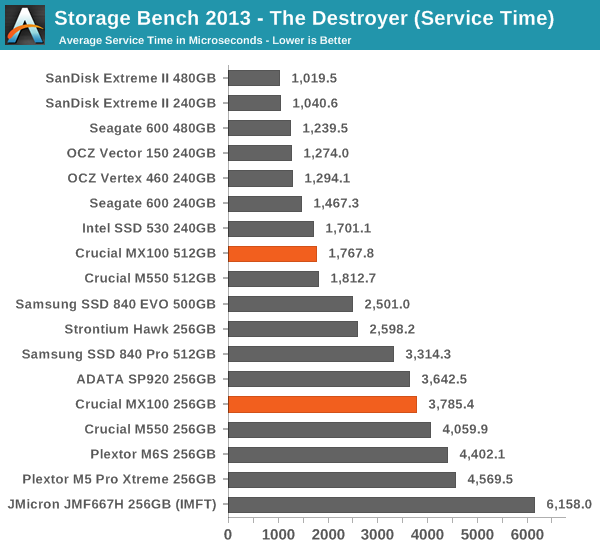
We are reporting two primary metrics with the Destroyer: average data rate in MB/s and average service time in microseconds. The former gives you an idea of the throughput of the drive during the time that it was running the test workload. This can be a very good indication of overall performance. What average data rate doesn't do a good job of is taking into account response time of very bursty (read: high queue depth) IO. By reporting average service time we heavily weigh latency for queued IOs. You'll note that this is a metric we have been reporting in our enterprise benchmarks for a while now. With the client tests maturing, the time was right for a little convergence.
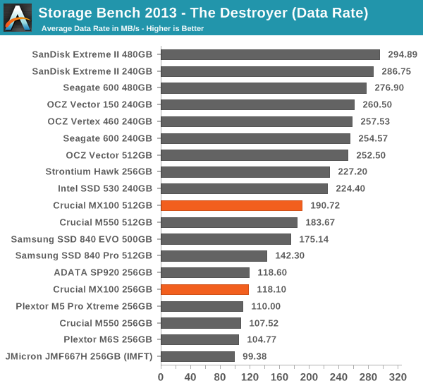
Quite surprisingly, the MX100 is slightly faster than the M550 in our 2013 Storage Bench. The differences are not significant, but it's still surprising given that M550 is supposed to be Crucial's higher performing drive. Especially at 256GB this is odd because the M550 has lower capacity NAND that should result in more parallelism and thus more performance, but that doesn't seem to be that case. I'm guessing that Crucial has been able to tweak the firmware to unleash more performance from the Marvell 9189 controller, which would explain why the MX100 is faster than the M550. Then again, the ADATA SP920 with 128Gbit NAND and Micron designed firmware is also faster than the 256GB M550, so it looks like M550 doesn't take full advantage of the lower capacity NAND.
AnandTech Storage Bench 2011
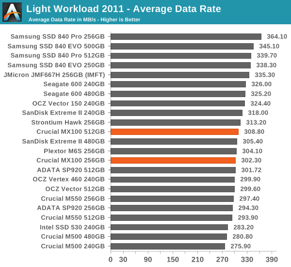
Back in 2011 (which seems like so long ago now!), we introduced our AnandTech Storage Bench, a suite of benchmarks that took traces of real OS/application usage and played them back in a repeatable manner. The MOASB, officially called AnandTech Storage Bench 2011 - Heavy Workload, mainly focuses on peak IO performance and basic garbage collection routines. There is a lot of downloading and application installing that happens during the course of this test. Our thinking was that it's during application installs, file copies, downloading and multitasking with all of this that you can really notice performance differences between drives. The full description of the Heavy test can be found here, while the Light workload details are here.
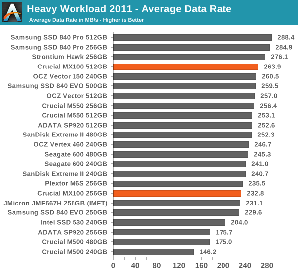
In our Heavy workload trace, the story changes. Now the 256GB M550 is faster than the 256GB MX100 but the 512GB MX100 still leads the Crucial pack. I'm thinking that the 256GB M550 is more optimized for non-steady-state operation as that's more common for client workloads, which would explain why it performs poorly in the 2013 bench but is better in the 2011 Heavy test. What's surprising is that the 256GB MX100 is much faster than the 256GB SP920 despite that fact that the only difference between them should be the NAND lithography. Maybe Micron/Crucial didn't give ADATA the highest performing firmware after all.
Random Read/Write Speed
The four corners of SSD performance are as follows: random read, random write, sequential read and sequential write speed. Random accesses are generally small in size, while sequential accesses tend to be larger and thus we have the four Iometer tests we use in all of our reviews.
Our first test writes 4KB in a completely random pattern over an 8GB space of the drive to simulate the sort of random access that you'd see on an OS drive (even this is more stressful than a normal desktop user would see). We perform three concurrent IOs and run the test for 3 minutes. The results reported are in average MB/s over the entire time.
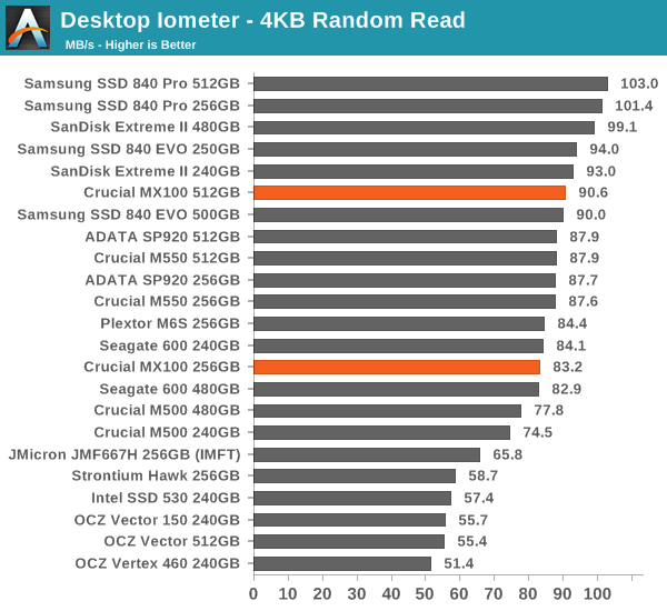
Random read performance remains mostly unchanged. The 512GB MX100 appears to be slightly faster than the M550 while the 256GB version is a few megabytes slower.
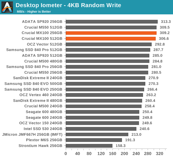
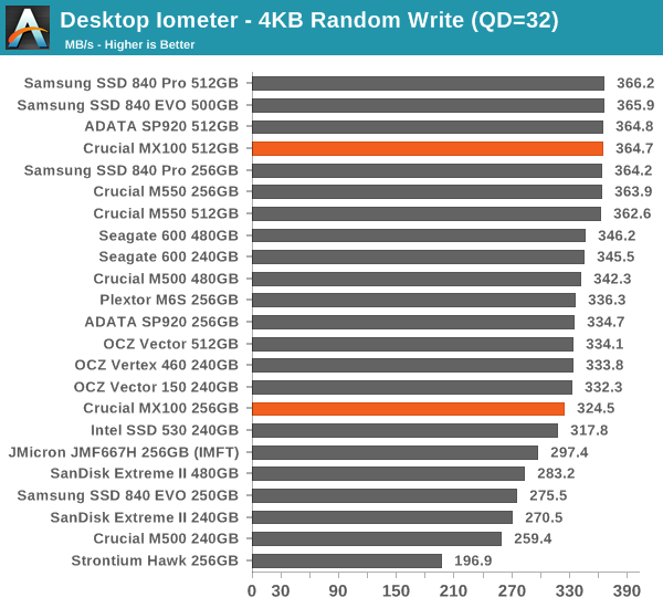
Random write performance, on the other hand, is slightly up at the lower queue depths. This is likely due to firmware optimizations as the performance is up regardless of the capacity, although once the queue depth is increased the 256GB version falls behind due to the more limited amount of NAND die.
Sequential Read/Write Speed
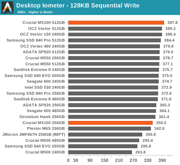
To measure sequential performance we run a 1 minute long 128KB sequential test over the entire span of the drive at a queue depth of 1. The results reported are in average MB/s over the entire test length.
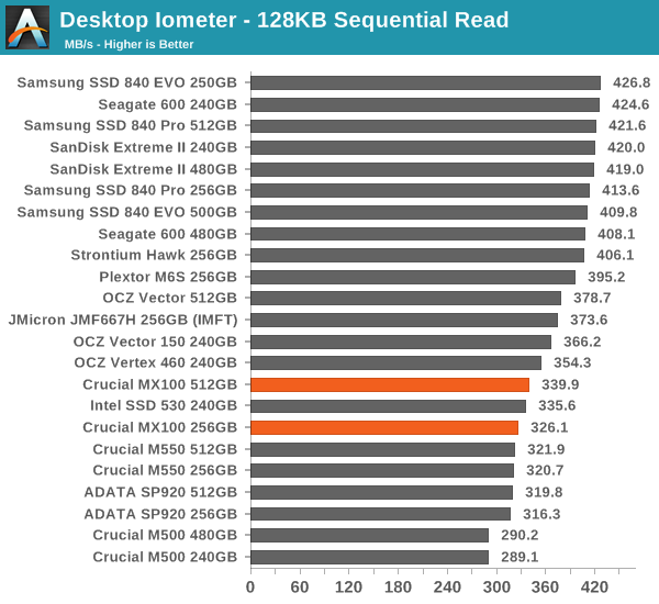
Sequential performance is also up by a bit, although the difference isn't dramatic.
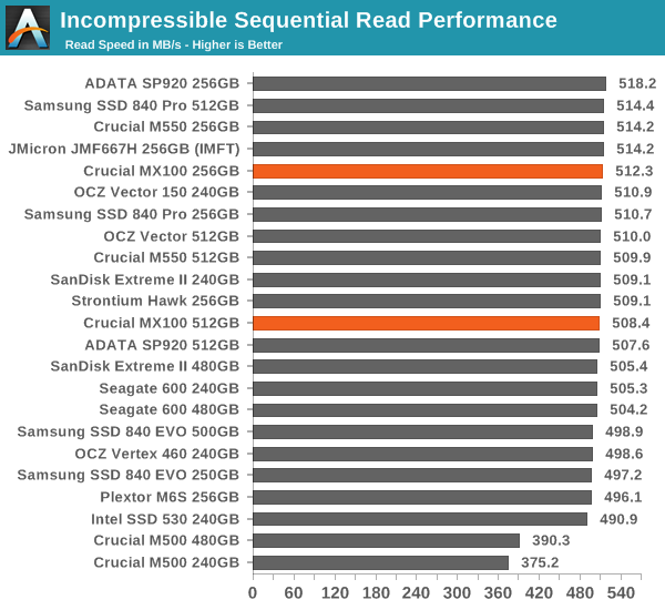
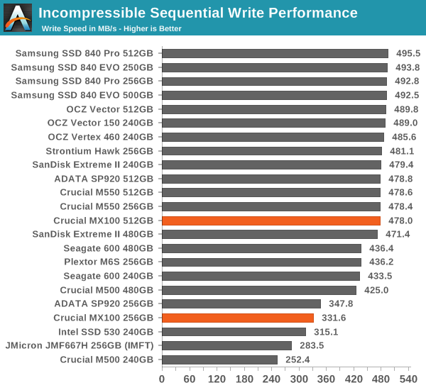
AS-SSD Incompressible Sequential Read/Write Performance
The AS-SSD sequential benchmark uses incompressible data for all of its transfers. The result is a pretty big reduction in sequential write speed on SandForce based controllers.
Performance vs. Transfer Size
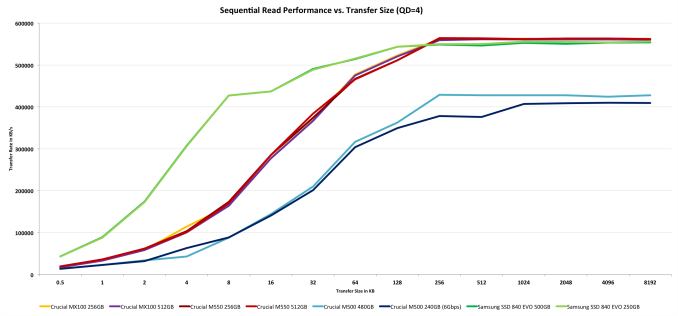
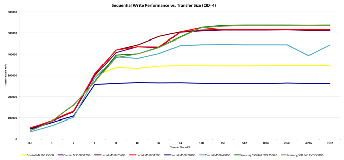
ATTO is a useful tool for quickly benchmarking performance across various transfer sizes. You can get the complete data set in Bench. Performance scaling appears to be identical to M550, which is a healthy upgrade from the M500 but still falls behind the 840 EVO in read performance.
Click for full size
Power Consumption
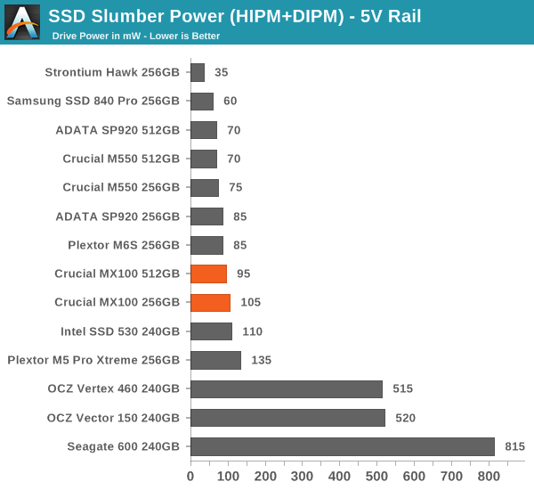
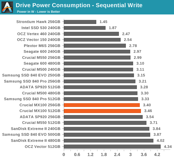
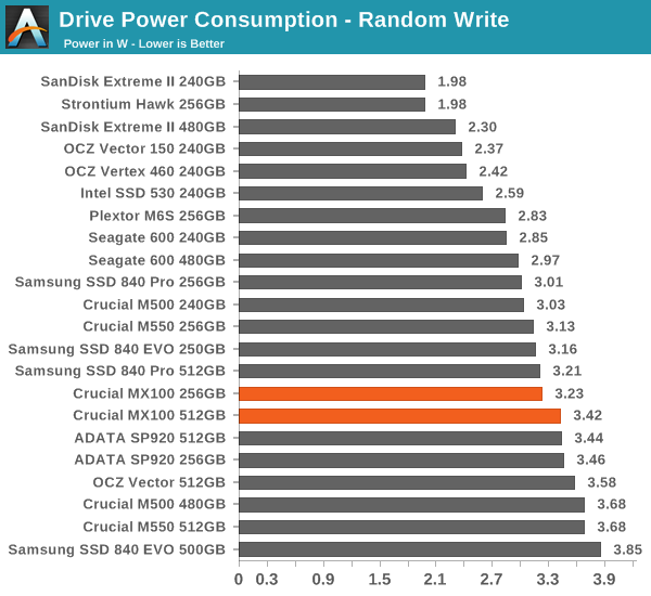
Like the M500 and M550, the MX100 supports DevSLP and slumber power states. Unfortunately we still don't have a way to measure DevSLP power but we do have slumber power results to report. Slumber power is actually up quite significantly, although the power consumption is still relatively low. Power consumption under load is, on the other hand, slightly down for the 512GB model whereas the 256GB MX100 consumes 0.1-0.4W more than its M550 counterpart.
Final Words
Shortly put, the MX100's task is to replace the M500 and it does that brilliantly. While the MX100's main goal is to lower the price by using smaller lithography NAND, it also provides a minor increase in performance over the M500 and offers the same industry-leading set of features. Given the success of the M500, Crucial had no reason to do a major overhaul with the MX100 and to be completely honest, there isn't really anything left to be desired. The performance and features are already present, so I really can't see how Crucial could make the MX100 significantly better. Sure the performance isn't record breaking but the MX100 isn't aimed at the enthusiast and professional segment where that is a concern.
My only criticism is towards the M550 and how it's positioned in the market. As I mentioned in the M550 review already, I don't really see where the drive fits in the market. It's not fast enough to compete in the enthusiast/professional space but on the other hand there is no reason for an average user to pay the premium for it, especially as the MX100 provides equivalent performance in nearly all scenarios. The 1TB M550 is the only model that makes sense but that is only because the MX100 tops out at 512GB; to be honest I would rather have a 1TB MX100 with the M550 being discontinued. I think the M550 as it currently stands doesn't really contribute anything to Crucial's SSD portfolio and all it does is cause confusion among potential buyers.
| NewEgg Price Comparison (6/2/2014) | ||||
| 120/128GB | 240/256GB | 480/512GB | ||
| Crucial MX100 (MSRP) | $80 | $110 | $225 | |
| Crucial M550 | $100 | $165 | $305 | |
| Crucial M500 | $72 | $110 | $230 | |
| Plextor M6S (MSRP) | $130 | $165 | $400 | |
| Plextor M5 Pro Xtreme | $200 | $230 | $459 | |
| ADATA Premier Pro SP920 | $90 | $150 | - | |
| Intel SSD 730 | - | $205 | $440 | |
| Intel SSD 530 | $110 | $165 | - | |
| OCZ Vector 150 | $115 | $200 | $339 | |
| OCZ Vertex 460 | $114 | $400 | $280 | |
| Samsung SSD 840 EVO | $110 | $181 | $280 | |
| Samsung SSD 840 Pro | $144 | $250 | $400 | |
| SanDisk Extreme II | $98 | $180 | $420 | |
| Seagate SSD 600 | $105 | $136 | $314 | |
And here's where the other shoe drops. The MSRPs (Manufacturer Suggested Retail Prices) are just insane; none of the big brands even come close to the prices of the MX100. You are basically getting a 256GB MX100 for the price of a 120/128GB SSD, which is awesome. Obviously these are not final prices but in my experience the MSRPs tend to be more conservative than aggressive, so final retail prices may end up being even lower. I wonder how Samsung in particular is going to respond because the 840 EVO should have a cost advantage due to the use of TLC NAND, but right now the EVO is priced $30 to $70 higher while not providing any substantial added value.
All in all, I have nothing negative to say about the MX100. With the performance and feature set, combined with pricing that basically doubles the amount of storage you get for your dollar, it's an absolute no-brainer. Unless you are an enthusiast or professional with a heavy IO workload, the MX100 is currently the drive with the best bang for the buck in the market by far.

