Original Link: https://www.anandtech.com/show/783
Gigabyte GA-7ZXR (Rev. 2.2) Socket-A KT133A ATX
by Mike Andrawes on June 7, 2001 2:34 AM EST- Posted in
- Motherboards
The motherboard industry is currently in one of those transition periods, where lots of new technologies are being introduced, but nobody really knows for sure which is the best or which will survive. On one hand, Intel’s Pentium 4 is pounding its way into the market with the i850 chipset’s dual channel RDRAM to provide sufficient memory bandwidth for their flagship processor. On the other hand, AMD and VIA are pushing hard for DDR to become the memory technology of the future.
While the new technologies do seem promising, it will still be a while before RDRAM and DDR SDRAM show their full potential, and that’s exactly why good old SDR SDRAM is still quite popular. The VIA KT133A chipset is the perfect example of this, as it still uses SDR SDRAM but delivers performance figures similar to the newer solutions.
It’s been a while since we last visited a KT133A motherboard, but we thought we’d take a look at an in-depth look at a few of the more popular ones before rounding them all up. Today we have Gigabyte’s solution, the GA-7ZXR (Rev. 2.2).
Back in November, during our second KT133 motherboard roundup, we took a brief look at the GA-7ZXR, Gigabyte’s first attempt in the Socket-A market. We concluded that it was a somewhat disappointing solution for two reasons - not only was it a merely average performer, but it lacked multiplier adjustments, a virtual requirement for overclocking a Socket-A processor and something that most other manufacturers had implemented.
However, as we have seen numerous times before, six months is an extremely long time in the computer industry, and a lot of changes can be made to a motherboard. Not long ago, we received word from Gigabyte that revision 2.2 of the GA-7ZXR would arrive soon, with the KT133A chipset along for the ride. Of course, we were eager to see just how this new revision compared to the old one.
The long wait is finally over and the newest GA-7ZXR revision has arrived in the AnandTech Labs. As expected, this board proves to be a much better solution than its older brother and is much more capable. The real question is “just how much better is it in terms of features and stability?” That’s exactly what we seek to answer in this review.
|
Gigabyte GA-7ZXR (2.2) |
|
|
CPU
Interface
|
Socket-A
|
|
Chipset
|
VIA
KT133A
VT 8363A North Bridge VT 686B South Bridge |
|
Form
Factor
|
ATX
|
|
Bus
Speeds
|
100
- 120 MHz (in 1 MHz increments) |
|
Core
Voltages Supported
|
Auto
Detect |
|
I/O
Voltages Supported
|
3.3
/ 3.4 / 3.5 V
|
|
AGP
Voltages Supported
|
1.5
/ 1.6 / 1.7 V
|
|
Memory
Slots
|
3
168-pin DIMM Slots
|
|
Expansion
Slots
|
1
AGP Slot |
|
On-board
Audio
|
Sigmatel
STA9708T AC97 CODEC
Creative CT5880 (optional) |
|
BIOS
|
AMI Simple BIOS Setup 1.24b |
A New Revision, A Slightly Different Look

The general layout of the GA-7ZXR (2.2) is more or less the same as the original, but with a few noticeable changes. Probably the most is the removal of the ISA slot and the insertion of a sixth PCI slot. This decision is better geared for the current market since legacy ISA devices have all but disappeared by now.
The original GA-7ZXR had quite a bit of unused PCB space on the bottom right hand corner, but not this time. That space has been replaced by a more robust voltage regulator module that should allow the GA-7XR revision 2.2 to support all upcoming Socket-A processors and possibly provide improved stability to boot.
There are also several new sets of dipswitches on the new revision,, indicating the possibility that Gigabyte has inserted some new tweaking options for the hardware enthusiasts out there. We’ll get to the details in a moment.
Like the original, the power supply connector is located in front of the DIMM slot, so you will not have to worry about the power cables running over the CPU or memory. Unfortunately, the CPU socket is located quite close to the right edge of the motherboard, which makes mounting or removing a HSF unit difficult once the board is seated inside a case.
All IDE and floppy connectors are located in front of the DIMM slots. Unlike some other designs, this setup does not block the use of long PCI or AGP devices. Another thing to look out for is the size of the GA-7ZXR (2.2). It measures in at 12 by 9.5 inches, which could be a tight fit in some cases. You should make sure that your case is deep enough for the board, or the drive bays may block the IDE and floppy connectors.
The Basics
The VIA 8363A
Gigabyte was one of the first to include an AGP retention mechanism on their boards, and the GA-7ZXR is no exception. It was implemented to prevent AGP cards from falling out of place during shipping after some OEM’s complained this was occurring too often.
The AGP retention mechanism
As mentioned
above, the 8363A
However, in order to do all of that, you need a motherboard that’s capable of adjusting the CPU multiplier ratio. Of course, you still need to prepare your CPU for overclocking, a subject we explored carefully with our Socket-A Athlon/Duron Overclocking Guide. Moreover, since the GA-7ZXR’s implementation uses dipswitches for both FSB and multiplier ratio, you should also read our KT133A Chipset: The Issue article to make sure you perform the overclocking correctly.
The GA-7ZXR (2.2) has a total of three DIMM slots supporting up to 1.5GB SDRAM. The memory controller allows you to run your memory at either 100MHz or 133MHz, depending on your FSB choice. When running in the 100MHz FSB range, you have the option to run your memory at host clock (FSB speed) or host clock + PCI clock. When the FSB is set to 133MHz or higher, the chipset only allows you to operate your memory synchronously with the FSB. That’s one of the specifications of the KT133A chipset, which supports FSB:memory bus ratios of 100:100, 100:133, and 133:133.
Like all other KT133A motherboards,
the GA-7ZXR (2.2) uses the VIA 686B
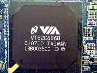
VIA’s 686B
The 686B also supports two USB root hubs. The first hub provides the two traditional USB ports found at the back of the motherboard as part of the ATX I/O panel. The second set of USB ports is located at the front edge of the board and requires the use of a USB bracket that is included in the box.
The 6/1/0/1 (PCI/AGP/ISA/AMR) expansion slot design is a very impressive decision by Gigabyte. The original version of the board featured a 5/1/1/1 configuration. At the time, the extra ISA slot was still useful for some users who were still hanging onto old ISA modems or SCSI controllers, but these users are becoming fewer and fewer everyday. Therefore, Gigabyte’s decision to take away the ISA slot, shift the AMR slot to the left, and include an extra PCI slot was probably a wise one. The six PCI slots provide much more flexibility, even if most won’t come close to using all the slots.
Gigabyte uses the Sigmatel STAC9708T AC‘97 host-based CODEC as their on-board audio solution, providing basic sound for a system. If you want true hardware-accelerated sound,, Gigabyte also offers an optional Creative CT5880 chip. The CT5880 is the same as that used in Creative’s Sound Blaster PCI line and is more than adequate for those that don’t require 3D spatial audio.
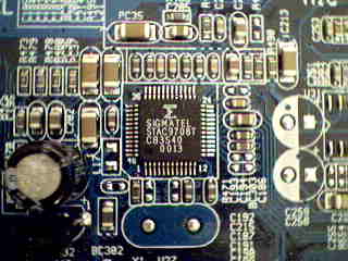
The Sigmatel ATAC9708T AC’97 CODEC
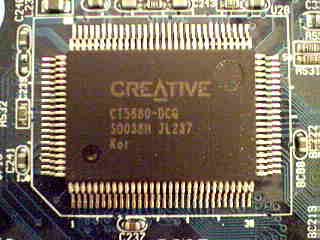
Optional Creative CT5880 sound
Making up the Loss
When we looked at the original GA-7ZXR, it took quite a big hit for its lack of overclocking features and it didn’t help that the stability was not particularly impressive either. At the time we did our roundup in November 2000, Gigabyte told us that they were working on a newer revision of the board, which would be quite different from the one we looked at, with more overclocking options.
When we received that message, we assumed that Gigabyte was referring to the “missing” multiplier ratio settings, which was present on most other KT133 boards. However, when we finally received the current revision of the GA-7ZXR, we concluded that we were wrong, as Gigabyte had included lots more features than just multiplier controls.
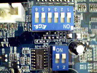
For starters, and the critical multiplier adjustments are included, with ratios between 5 and 12.5 (in 0.5 increments), configured through a set of five dipswitches. The setting is not available in the BIOS, but from our KT133A Chipset: the Issue article, we know that a dipswitch implementation is indeed very reliable.
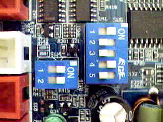
Dipswitches for modifying the multiplier and I/O voltage
Like the original, there is another set of five dipswitches controlling the FSB speeds. Using the set of dipswitches you can choose from 95 / 100 / 102 / 105 / 110 / 113 / 115 / 120 / 133 / 135 / 137 / 139 / 141 / 143 / 145 / 150 / 155 / 160 / 200 MHz. Although this list is already much longer than the speeds available last time around, this time there’s also the option of adjusting the FSB right in the BIOS.
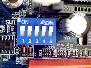
The dipswitch block for setting the FSB speed
The way the BIOS settings work is dependant on the FSB speed set using the dipswitches. If the FSB dipswitches are set between 95 and 100MHz, BIOS offers speeds between 100MHz and 120MHz in 1MHz increments. On the other hand, if you set the dipswitches to 133MHz or higher, you will be able to choose any speed between 133MHz and 150MHz in the BIOS, also in 1MHz increments. The inclusion of FSB speed adjustment in the BIOS is definitely nice, but it’s the new 1MHz implementation that truly puts the GA-7ZXR (2.2) among the top KT133A boards when it comes to overclocking.
Apart from multiplier ratio and FSB speed settings, voltage tweaks are another important factor for overclocking, and Gigabyte has covered this as well. For CPU core voltage, you can select between 1.5V and 1.85V in 0.025V increments through a set of six dipswitches. For I/O voltage, the GA-7ZXR (2.2) allows you to select between 3.3 / 3.4 / 3.5V using two dipswitches. Furthermore, Gigabyte also decided to put in AGP voltage tweaks, allowing you to choose from 1.5 / 1.6 / 1.7V.
The dipswitches for adjusting the CPU core and AGP voltages
Features and Overclocking
Unlike a few other boards out there, the GA-7ZXR (2.2) features
just a heatsink on the
Our tests results show that without any voltage tweaks, the GA-7ZXR (2.2) was able to run the FSB at 145MHz without losing any stability. By changing the memory timing and turning up the I/O and AGP voltages, we were able to achieve 147MHz. Any higher speed prevented the system from completing POST at all. This is around a 10% overclock for the 8363A, which is not very impressive since we have seen some boards doing more than 160MHz, which is about a 20% overclocking.
As mentioned earlier, the stability of the original GA-7ZXR was not particularly impressive, leaving lots of room for improvement. The revision 2.2 board we have here is very different. With the insertion of a few more MOSFETs and 1200uF capacitors, the board crashed a total of two times in 24 hours during our stress tests. This is not the most impressive result we have seen among other KT133A boards, but it’s quite good overall anyway. Furthermore, by playing with the I/O and AGP voltages, we were able to run the stability tests for 24 hours with only one crash, showing that the voltage tweaking options do help to maintain the stability of the system.

The added capacitors and MOSFETs in the bottom right hand corner
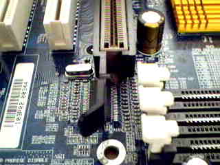
Also like the original board, revision 2.2 also features
an optional Promise Ultra ATA 100 IDE RAID controller. Gigabyte chose the PDC20265R
controller, which supports both RAID 0 and RAID 1 configurations. If you don’t
intend to use the RAID functionality, you can also use the controller as a second
Ultra ATA 100 controller, supporting two more IDE channels and up to four IDE
devices. Combined with the two IDE controllers of the 686B

The Promise Ultra ATA 100 IDE RAID controller
Also like many other Gigabyte products, the GA-7ZXR (2.2) features their Dual BIOS setup. Basically, Gigabyte includes two BIOS chips on the motherboard, and in the case of virus BIOS corruption, the backup BIOS is automatically used to boot the system, allowing you to recover the system without any downtime.
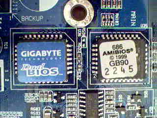
Gigabyte’s Dual BIOS chips
Unfortunately, Gigabyte did not include jumpers for clearing the CMOS, something we’ve seen a few other manufacturers do in the past. Instead, you have to use a flathead screwdriver to short two solder pads to clear the CMOS, which is somewhat inconvenient. We’ve seen a couple other manufacturers do this before, most notably ASUS, and there’s no clear reason for it other than to make it more difficult to reset the CMOS.
Even the manual has been improved quite a bit, providing more detail on RAID setup and driver / utility installation. Although it’s still not quite at the level of those by ABIT or ASUS, we can see that Gigabyte has put quite a bit of effort in constructing the manual.
The Test
In recent times, choosing a motherboard cannot be completely determined by a Winstone score. Now, many boards come within one Winstone point of each other and therefore the need to benchmark boards against each other falls. Therefore you should not base your decision entirely on the benchmarks you see here, but also on the technical features and advantages of this particular board, seeing as that will probably make the greatest difference in your overall experience.
|
Test Configuration |
|
| Processor(s): |
AMD
Athlon (Thunderbird) 1GHz
|
| RAM: |
1x 128MB Mushkin PC133 SDRAM
|
| Hard Drive(s): |
Western Digital 153BA Ultra ATA
66 7200 RPM
|
| Bus Master Drivers: |
VIA 4-in-1 v4.24 Service Pack
|
| Video Card(s): |
NVIDIA
GeForce 2 GTS 32MB DDR
|
| Video Drivers: |
NVIDIA
Detonator 5.22
|
| Operation System(s): |
Windows
98SE
|
| Motherboard Revision: |
Gigabyte
7ZXR Revision 2.2
|
|
BIOS
Revision:
|
FA6
(3/8/2001)
|
The Results
|
Windows 98 Performance |
|||
|
Athlon
1GHz OEM
KT133A / 133 MHz |
Sysmark
2000
|
Content
Creation
Winstone 2001 |
Quake
III Arena - 640 x 480 x 16
|
| Gigabyte 7ZXR (2.2) |
196
|
36.7
|
142.9
|
| AOpen AK73 ProA |
199
|
37.3
|
152.4
|
| Iwill KK266 |
197
|
37.0
|
152.7
|
| ASUS A7V133 |
197
|
37.6
|
153.4
|
| MSI K7T Turbo |
194
|
37.5
|
145.7
|
| EPoX EP-8KTA3 |
196
|
36.7
|
146.3
|
| ABIT KT7A-RAID |
197
|
37.4
|
149.6
|
Gigabyte motherboards have never been outstanding performers, and the GA-7ZXR (2.2) actually fell to last place as the slowest KT133A boards we have looked at. The board did score higher than the MSI K7T Turbo in SYSMark 2000 by 1%, but it fell behind in both Content Creation Winstone 2000 and Quake III Arena as the slowest. Howerver, note that all boards still perform within a few percentage points of each other, so performance should not be a major concern.
Final Words
Gigabyte probably could have done themselves a favor by giving this board a different name to help distinguish it from their KT133 solution more clearly. Nevertheless, the name certainly doesn’t hurt what this board is capable of doing. The GA-7ZXR (2.2) is not the best KT133A board we have looked at, but it’s definitely among the top. Performance is definitely something Gigabyte should work on to make sure it performs up to par with other KT133A boards out there, but the biggest problem with the GA-7ZXR (2.2) is the time of release. Released in March, the GA-7ZXR is two months late compared to some of the best KT133A motherboards, and it might just be too little too late after all, especially with AMD 760 and KT266 boards hitting the streets already.
Nevertheless, if we let the board stand on its own merits, it’s clear that Gigabyte has put a lot of effort into the GA-7ZXR (2.2) and indeed has made the board very competitive thanks to excellent features and stability. The addition of the multiplier ratio settings is certainly curcial, but it’s the ability for 1MHz increments for FSB speed that truly make this board a good choice for overclockers. Gigabyte also provides reasonable ranges for voltage tweaking of the CPU, I/O, and AGP. Of course the added flexibility provided by the onboard Promise IDE RAID controller is more than welcome.
All in all, the GA-7ZXR (2.2) is a very nice KT133A motherboard, that could have captured much more of the market had it been released earlier.
How it Rates
|
AnandTech Motherboard Rating |
|
|
Rating
(x/10)
|
|
|
Performance
|
4.5
|
|
Price
|
5.0
|
|
Stability
|
8.0
|
|
Features
|
8.5
|
|
Layout
|
7.5
|
|
Availability
|
6.5
|
|
Documentation & Software Bundle
|
7.0
|
| Overall Rating - not an average Click here to find out why |
8.0
|


