Original Link: https://www.anandtech.com/show/7764/the-nvidia-geforce-gtx-750-ti-and-gtx-750-review-maxwell
The NVIDIA GeForce GTX 750 Ti and GTX 750 Review: Maxwell Makes Its Move
by Ryan Smith & Ganesh T S on February 18, 2014 9:00 AM EST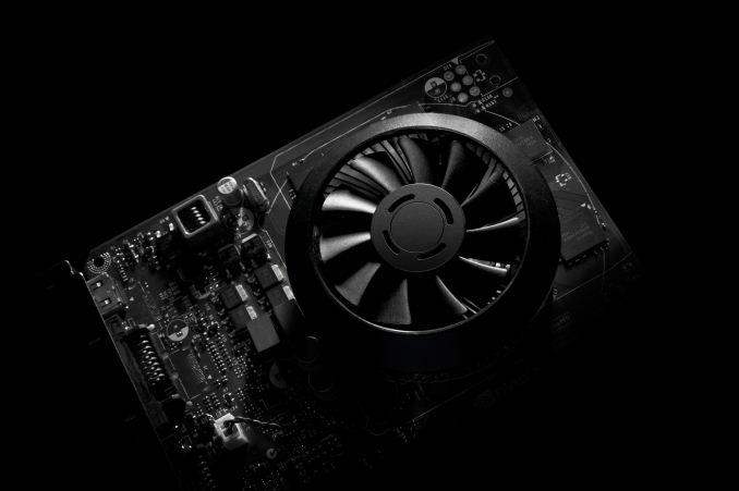
As the GPU company who’s arguably more transparent about their long-term product plans, NVIDIA still manages to surprise us time and time again. Case in point, we have known since 2012 that NVIDIA’s follow-up architecture to Kepler would be Maxwell, but it’s only more recently that we’ve begun to understand the complete significance of Maxwell to the company’s plans. Each and every generation of GPUs brings with it an important mix of improvements, new features, and enhanced performance; but fundamental shifts are fewer and far between. So when we found out Maxwell would be one of those fundamental shifts, it changed our perspective and expectations significantly.
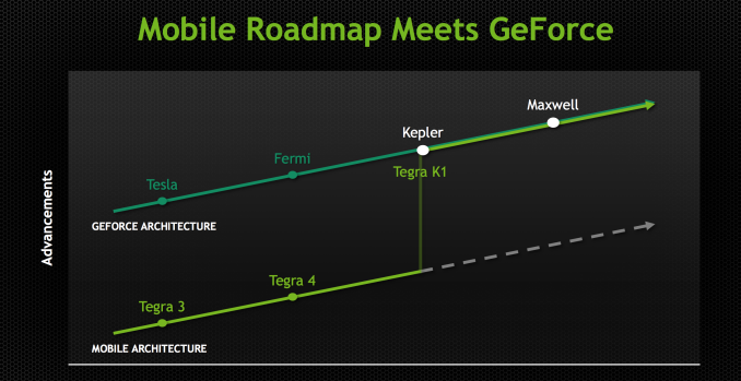
What is that fundamental shift? As we found out back at NVIDIA’s CES 2014 press conference, Maxwell is the first NVIDIA GPU that started out as a “mobile first” design, marking a significant change in NVIDIA’s product design philosophy. The days of designing a flagship GPU and scaling down already came to an end with Kepler, when NVIDIA designed GK104 before GK110. But NVIDIA still designed a desktop GPU first, with mobile and SoC-class designs following. However beginning with Maxwell that entire philosophy has come to an end, and as NVIDIA has chosen to embrace power efficiency and mobile-friendly designs as the foundation of their GPU architectures, this has led to them going mobile first on Maxwell. With Maxwell NVIDIA has made the complete transition from top to bottom, and are now designing GPUs bottom-up instead of top-down.
Nevertheless, a mobile first design is not the same as a mobile first build strategy. NVIDIA has yet to ship a Kepler based SoC, let alone putting a Maxwell based SoC on their roadmaps. At least for the foreseeable future discrete GPUs are going to remain as the first products on any new architecture. So while the underlying architecture may be more mobile-friendly than what we’ve seen in the past, what hasn’t changed is that NVIDIA is still getting the ball rolling for a new architecture with relatively big and powerful GPUs.
This brings us to the present, and the world of desktop video cards. Just less than 2 years since the launch of the first Kepler part, the GK104 based GeForce GTX 680, NVIDIA is back and ready to launch their next generation of GPUs as based on the Maxwell architecture.
No two GPU launches are alike – Maxwell’s launch won’t be any more like Kepler’s than Kepler was Fermi’s – but the launch of Maxwell is going to be an even greater shift than usual. Maxwell’s mobile-first design aside, Maxwell also comes at a time of stagnation on the manufacturing side of the equation. Traditionally we’d see a new manufacturing node ready from TSMC to align with the new architecture, but just as with the situation faced by AMD in the launch of their GCN 1.1 based Hawaii GPUs, NVIDIA will be making do on the 28nm node for Maxwell’s launch. The lack of a new node means that NVIDIA would either have to wait until the next node is ready, or launch on the existing node, and in the case of Maxwell NVIDIA has opted for the latter.
As a consequence of staying on 28nm the optimal strategy for releasing GPUs has changed for NVIDIA. From a performance perspective the biggest improvements still come from the node shrink and the resulting increase in transistor density and reduced power consumption. But there is still room for maneuvering within the 28nm node and to improve power and density within a design without changing the node itself. Maxwell in turn is just such a design, further optimizing the efficiency of NVIDIA’s designs within the confines of the 28nm node.
With the Maxwell architecture in hand and its 28nm optimizations in place, the final piece of the puzzle is deciding where to launch first. Thanks to the embarrassingly parallel nature of graphics and 3D rendering, at every tier of GPU – from SoC to Tesla – GPUs are fundamentally power limited. Their performance is constrained by the amount of power needed to achieve a given level of performance, whether it’s limiting clockspeed ramp-ups or just building out a wider GPU with more transistors to flip. But this is especially true in the world of SoCs and mobile discrete GPUs, where battery capacity and space limitations put a very hard cap on power consumption.
As a result, not unlike the mobile first strategy NVIDIA used in designing the architecture, when it comes to building their first Maxwell GPU NVIDIA is starting from the bottom. The bulk of NVIDIA’s GPU shipments have been smaller, cheaper, and less power hungry chips like GK107, which for the last two years has formed the backbone of NVIDIA’s mobile offerings, NVIDIA’s cloud server offerings, and of course NVIDIA’s mainstream desktop offerings. So when it came time to roll out Maxwell and its highly optimized 28nm design, there was no better and more effective place for NVIDIA to start than with the successor to GK107: the Maxwell based GM107.
Over the coming months we’ll see GM107 in a number of different products. Its destiny in the mobile space is all but set in stone as the successor to the highly successful GK107, and NVIDIA’s GRID products practically beg for greater efficiency. But for today we’ll be starting on the desktop with the launch of NVIDIA’s latest desktop video cards: GeForce GTX 750 Ti and GeForce GTX 750.
Maxwell’s Feature Set: Kepler Refined
To start our look at the Maxwell architecture, we’ll start with a look at the feature set, as this will be the shorter and easier subject to begin with.
In short, Maxwell only offers a handful of new features compared to Kepler. Kepler itself was a natural evolution of Fermi, further building on NVIDIA’s SM design and Direct3D 11 functionality. Maxwell in turn is a smaller evolution yet.
From a graphics/gaming perspective there will not be any changes. Maxwell remains a Direct3D 11.0 compliant design, supporting the base 11.0 functionality along with many (but not all) of the features required for Direct3D 11.1 and 11.2. NVIDIA as a whole has not professed much of an interest in being 11.1/11.2 compliant – they weren’t in a rush on 10.1 either – so this didn’t come as a great surprise to us. Nevertheless it is unfortunate, as NVIDIA carries enough market share that their support (or lack thereof) for a feature is often the deciding factor whether it’s used. Developers can still use cap bits to access the individual features of D3D 11.1/11.2 that Maxwell does support, but we will not be seeing 11.1 or 11.2 becoming a baseline for PC gaming hardware this year.
On the other hand this means that for the purposes of the GeForce family the GTX 750 series will fit in nicely into the current stack, despite the architectural differences. As a consumer perspective is still analogous to a graphics perspective, Maxwell does not have any features that will explicitly set it apart from Kepler. All 700 series parts will support the same features, even NVIDIA ecosystem features such as GameWorks, NVENC, and G-Sync, so Maxwell is fully aligned with Kepler in that respect.
At a lower level the feature set has only changed to a slightly greater degree. I/O functionality is identical to Kepler, with 4 display controllers backing NVIDIA’s capabilities. HDMI 1.4 and DisplayPort 1.2 functionality join the usual DVI support, with Maxwell being a bit early to support any next generation display connectivity standards.
Video Encode & Decode
Meanwhile turning our gaze towards video encoding and decoding, we find one of the few areas that has received a feature upgrade on Maxwell. NVENC, NVIDIA’s video encoder, has received an explicit performance boost. NVIDIA tells us that Maxwell’s NVENC should be 1.5x-2x faster than Kepler’s NVENC, or in absolute terms capable of encoding speeds 6x-8x faster than real time.
For the purposes of the GTX 750 series, the impact of this upgrade will heavy depend on how NVENC is being leveraged. For real time applications such as ShadowPlay and GameStream, which by the very definition can’t operate faster than real time, the benefit will primarily be a reduction in encoding latency by upwards of several milliseconds. For offline video transcoding using utilities such as Cyberlink’s MediaEspresso, the greater throughput should directly translate into faster transcoding.
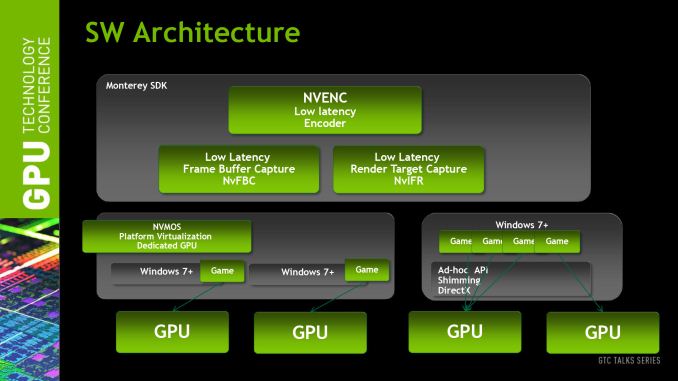
The bigger impact of this will be felt in mobile and server applications, when GM107 makes its introduction in those product lines. In the case of mobile usage the greater performance of Maxwell’s NVENC block directly corresponds with lower power usage, which will reduce the energy costs of using it when operating off of a battery. Meanwhile in server applications the greater performance will allow a sliding scale of latency reductions and an increase in the number of client sessions being streamed off of a single GPU, which for NVIDIA’s purposes means they will get to increase the client density of their GRID products.
Speaking of video, decoding is also receiving a bit of a lift. Maxwell’s VP video decode block won’t feature full H.265 (HEVC) support, but NVIDIA is telling us that they will offer partial hardware acceleration, relying on a mix of software and hardware to decode H.265. We had been hoping for full hardware support on Maxwell, but it looks like it’s a bit premature for that in a discrete GPU. The downside to this is that the long upgrade cycle for video cards – many users are averaging 4 years these days – means there’s a good chance that GTX 750 owners will still be on their GTX 750 cards when H.265 content starts arriving in force, so it will be interesting to see just how much of the process NVIDIA can offload onto their hardware as it stands.
H.265 aside, video decoding overall is getting faster and lower power. NVIDIA tells us that decoding is getting a 8x-10x performance boost due to the implementation of a local decoder cache and an increase in memory efficiency for video decoding. As for power consumption, combined with the aforementioned performance gains, NVIDIA has implemented a new power state called “GC5” specifically for low usage tasks such as video playback. Unfortunately NVIDIA isn’t telling us much about how GC5 works, but as we’ll see in our benchmarks there is a small but distinct improvement in power consumption in the video decode process.
Maxwell: Designed For Energy Efficiency
While Maxwell doesn’t come with a significant overhaul of its high level feature set, the same cannot be said for the low level design of Maxwell. In fact the consistency at a high level betrays just how much work NVIDIA has done under the hood in order to improve their efficiency for Maxwell. Maxwell isn’t a complete overhaul of NVIDIA’s designs, nor is it even as aggressive as Kepler was when it eliminated Fermi’s hot clocks in favor of a wider design, but it has a number of changes that are important to understanding the architecture and more importantly understanding how NVIDIA is achieving their efficiency goals.
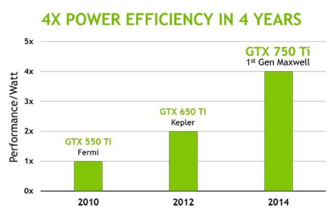
Broadly speaking, with Maxwell NVIDIA is almost solely focused on improving energy efficiency and performance per watt. This extends directly from NVIDIA’s mobile first design strategy for Maxwell, where the company needs to maximize energy efficiency in order to compete and win within the mobile space. If NVIDIA can bring down their energy consumption, then due to the power limiting factor we mentioned earlier they can use that recovered power overhead to further improve their performance. This again being especially noticeable in SoC-class products and discrete mobile due to the low power budgets these platforms provide.
To a lesser extent NVIDIA is also focused on space efficiency. GPU production costs and space efficiency go hand-in-hand, so there’s an interest in improving the density of their designs with Maxwell. This is especially the case when the earlier power savings allow for a wider GPU with a larger number of functional units within the same power envelope. Denser designs allow for NVIDIA to offer similar performance as larger Kepler GPUs (e.g. GK106) with a smaller Maxwell GPU.
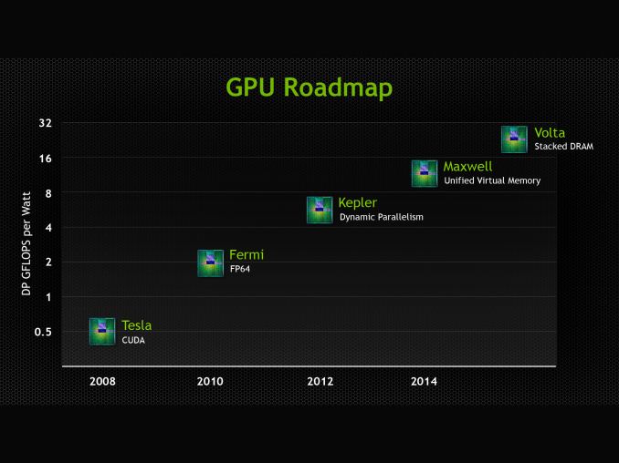
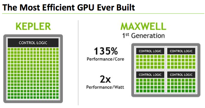
To achieve this NVIDIA has taken a number of steps, some of which they’ve shared with us at a high level and some of which they haven’t. NVIDIA is taking a bit of a “secret sauce” approach to Maxwell from a design level, so while we know a fair bit about its execution model we don’t know quite as much about the little changes that add up to Maxwell’s energy and space savings. However NVIDIA tells us that overall they’ve been able to outright double their performance-per-watt on Maxwell versus Kepler, which is nothing short of amazing given the fact that all of this is being done on the same 28nm process as Kepler.
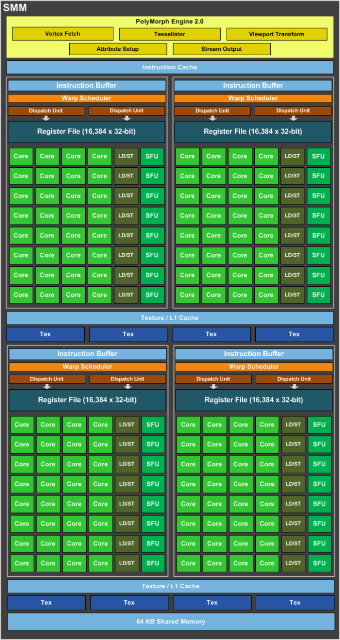
We’ll go over execution flow and the other gritty details on the next page, but for now let’s start with a look at NVIDIA’s Streaming Multiprocessor designs for Kepler (SMX) and Maxwell (SMM).
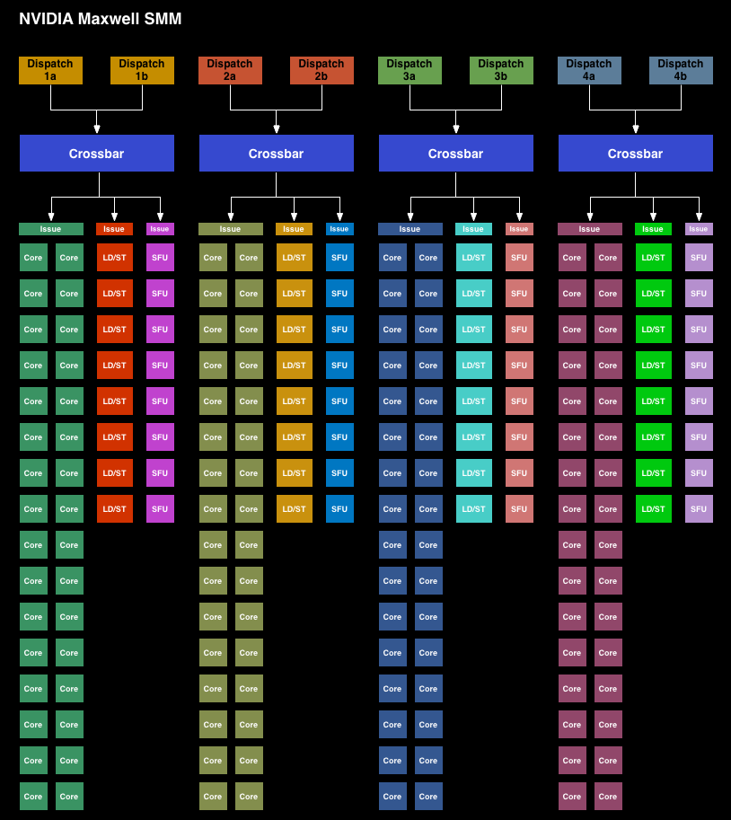
Immediately we can see a significant difference in the layout between the SMX and the new SMM. Whereas the SMX was for all practical purposes a large, flat design with 4 warp schedulers and 15 different execution blocks, the SMM has been heavily partitioned. Physically each SMM is still one contiguous unit, not really all that different from an SMX. But logically the execution blocks which each warp scheduler can access have been greatly curtailed.
The end result is that in an SMX the 4 warp schedulers would share most of their execution resources and work out which warp was on which execution resource for any given cycle. But on an SMM, the warp schedulers are removed from each other and given complete dominion over a far smaller collection of execution resources. No longer do warp schedulers have to share FP32 CUDA cores, special function units, or load/store units, as each of those is replicated across each partition. Only texture units and FP64 CUDA cores are shared.
Among the changes NVIDIA made to reduce power consumption, this is among the greatest. Shared resources, though extremely useful when you have the workloads to fill them, do have drawbacks. They’re wasting space and power if not fed, the crossbar to connect all of them is not particularly cheap on a power or area basis, and there is additional scheduling overhead from having to coordinate the actions of those warp schedulers. By forgoing the shared resources NVIDIA loses out on some of the performance benefits from the design, but what they gain in power and space efficiency more than makes up for it.
NVIDIA hasn’t given us hard numbers on SMM power efficiency, but for space efficiency a single 128 CUDA core SMM can deliver 90% of the performance of a 192 CUDA core SMX at a much smaller size.
Moving on, along with the SMM layout changes NVIDIA has also made a number of small tweaks to improve the IPC of the GPU. The scheduler has been rewritten to avoid stalls and otherwise behave more intelligently. Furthermore by achieving higher utilization of their existing hardware, NVIDIA doesn’t need as many functional units to hit their desired performance targets, which in turn saves on space and ultimately power consumption.
While on the subject of performance efficiency, NVIDIA has also been working on memory efficiency too. From a performance perspective GDDR5 is very powerful, however it’s also very power hungry, especially in comparison to DDR3. With GM107 in particular being a 128-bit design that would need to compete with the likes of the 192-bit GK106, NVIDIA has massively increased the amount of L2 cache they use, from 256KB in GK107 to 2MB on GM107. This reduces the amount of traffic that needs to cross the memory bus, reducing both the power spent on the memory bus and the need for a larger memory bus altogether.
Increasing the amount of cache always represents an interesting tradeoff since cache is something of a known quantity and is rather dense, but it’s only useful if there are memory stalls or other memory operations that it can cover. Consequently we often see cache implemented in relation to whether there are any other optimizations available. In some cases it makes more sense to use the transistors to build more functional units, and in other cases it makes sense to build the cache. After staying relatively stagnant on their cache sizes for so long, it looks like the balance has finally shifted and the cache increase makes the most sense for NVIDIA.
Of course even these changes are relatively high level from an ASIC perspective. There’s always the possibility for low-level changes and NVIDIA has followed through on these too. Case in point, both NVIDIA and AMD have been steadily improving their clock gating capabilities, and with Maxwell NVIDIA has taken another step in their designs. NVIDIA isn’t telling us just how fine grained their gating is now for Maxwell, but it’s a finer granularity than it was on Kepler. Given the new SM design, the most likely change was likely the ability to control the individual partitions and/or the functional units within those partitions, but this is just supposition on our part.
Finally there’s the lowest of low level optimizations, which is transistor level optimizations. Again NVIDIA hasn’t provided a ton of details here, but they tell us they’ve gone through at the transistor level to squeeze out additional energy efficiency as they could find it. Given that TSMC 28nm is now a very mature process with well understood abilities and quirks, NVIDIA should be able to design and build their circuits to a tighter tolerance now than they would have been able to when working on GK107 over 2 years ago.
GeForce GTX 750 Ti & GTX 750 Specifications & Positioning
Having finally covered the architecture and design choices of Maxwell in-depth, let’s talk about the retail hardware itself. As me mentioned in our introduction NVIDIA’s first play with Maxwell will be the high volume markets that GK107 resides in. Ultimately this means we should end up seeing GM107 in mobile GeForce and in server GRID products too, but first NVIDIA is starting with the desktop video card market. The desktop market affords NVIDIA the chance to take more direct control, so while server and mobile products go through additional phases of OEM/partner validation, desktop can be the first up to bat.
In a move a bit different from usual for an NVIDIA desktop video card launch, NVIDIA is launching multiple GM107 cards at once. Typically they’d stretch this out over a couple of weeks, but with the 700 series already on the market (and nothing better to do with salvaged chips) there’s little reason to wait.
| NVIDIA GPU Specification Comparison | ||||||
| GTX 660 | GTX 750 Ti | GTX 750 | GTX 650 | |||
| CUDA Cores | 960 | 640 | 512 | 384 | ||
| Texture Units | 80 | 40 | 32 | 32 | ||
| ROPs | 24 | 16 | 16 | 16 | ||
| Core Clock | 980MHz | 1020MHz | 1020MHz | 1058MHz | ||
| Boost Clock | 1033MHz | 1085MHz | 1085MHz | N/A | ||
| Memory Clock | 6GHz GDDR5 | 5.4GHz GDDR5 | 5GHz GDDR5 | 5GHz GDDR5 | ||
| Memory Bus Width | 192-bit | 128-bit | 128-bit | 128-bit | ||
| VRAM | 2GB | 2GB | 1GB | 1GB | ||
| FP64 | 1/24 | 1/32 | 1/32 | 1/24 | ||
| TDP | 140W | 60W | 55W | 64W | ||
| Transistor Count | 2.54B | 1.87B | 1.87B | 1.3B | ||
| Manufacturing Process | TSMC 28nm | TSMC 28nm | TSMC 28nm | TSMC 28nm | ||
| Architecture | Kepler | Maxwell | Maxwell | Kepler | ||
| GPU | GK106 | GM107 | GM107 | GK107 | ||
| Launch Date | 09/13/12 | 02/18/14 | 02/18/14 | 09/13/12 | ||
| Launch Price | $229 | $149 | $119 | $109 | ||
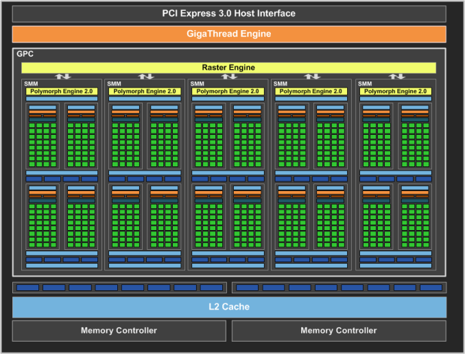
Starting with the GeForce GTX 750 Ti, this is NVIDIA’s flagship GM107 product. GTX 750 Ti packs a complete GM107 implementation, comprising 5 SMMs, 640 CUDA cores, 16 ROPs, and 40 texture units, and fed by 2MB of L2 cache. In terms of design GM107 is a clear successor to GK107, as evidenced by use of just 16 ROPs.
Nevertheless it’s very important to keep in mind that thanks to the Maxwell architecture GM107 hits well above its weight, so the CUDA core count difference between the GTX 750 Ti and GTX 660 makes these parts look much farther apart than they actually are. At least so long as we’re comparing Kepler and Maxwell parts, the product number is going to be the more meaningful designation as specs alone will not capture the relative power and efficiency of these designs.
GTX 750 Ti’s GM107 GPU is in turn paired with 2GB of GDDR5, on a 128-bit bus. The use of 2GB of VRAM is common for cards at this price range, whereas the 128-bit bus is narrower than competing cards, but something NVIDIA doesn’t expect to be badly hindered by due to their efficiency improvements elsewhere. On the other hand the company also expects some of its partners to roll out a smaller numbers of 1GB cards in the near future, and while these will be $10 cheaper we’re of the opinion that there’s no reason to have less than 2GB of VRAM on a card in this price range.
When it comes to clockspeeds NVIDIA will be shipping GTX 750 Ti and its GM107 GPU at slightly higher clockspeeds than its Kepler counterparts. NVIDIA is putting the core clock at 1020MHz with an official boost clock of 1085MHz; and as this is a GPU Boost 2.0 we’ll see the highest boost bins top out well over 1100MHz. The VRAM on the other hand will be clocked at 5.4GHz, which on a 128-bit bus is enough to provide 86.4GB/sec of memory bandwidth. The use of 5.4GHz RAM here is a bit off an oddity since no one produces GDDR5 RAM at that speed bin – these cards will have to be equipped with 6GHz RAM in order to meet the required specifications – so we strongly suspect this is a board limitation, especially since the board is virtually identical to NVIDIA’s board design for GTX 650 Ti, which also has the same 5.4GHz memory clock.
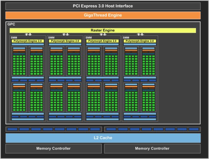
Switching gears for a moment, let’s now cover the GTX 750. GTX 750 is based on a cut-down/salvaged GM107 GPU, utilizing just 4 of GM107’s 5 SMMs. This reduces the CUDA core count to 512 and the number of texture units to 32, but it leaves the ROP/L2/memory partitions fully intact. GPU clockspeeds are identical to GTX 750 Ti – 1020MHz base, 1085MHz boost – while the memory subsystem is further reduced to 1GB of GDDR5 running at 5GHz. As such, the GTX 750 will fall behind the 750 Ti by anywhere between 8% and 20%, depending on whether the workload being measured is memory bound or shader/texture bound.
But perhaps the most impressive metric is power consumption. Due to NVIDIA’s optimizations efforts and 2x perf-per-watt goal for Maxwell, power consumption is way down versus the GK106 based parts that the GTX 750 and GTX 750 Ti will be replacing. NVIDIA’s official TDP – which is generally comparable within the NVIDIA product lineup – is just 60W for GTX 750 Ti, and a lower still 55W for GTX 750. For the sake of comparison this is a bit lower than either GTX 650 or GT 640 (the desktop GK107 parts), and more importantly these new GTX 750 series cards are quite a bit more powerful than the GK107 cards at similar TDPs.
The end result is that we’re looking at either a significant reduction in power consumption for similar performance to GK106, or a massive increase in performance as compared to GK107. Given the power limited nature of mobile in particular, this makes GM107 an especially potent GPU for NVIDIA.
With that in mind, it’s interesting to note that all of this comes despite the fact that both transistor counts and die sizes are up compared to GK107. GK107 was 118mm2 for 1.3 billion transistors, and meanwhile GM107 is 148mm2 for 1.87B transistors. The fact that NVIDIA was able to increase their transistor count by 43% has a lot to with how much faster GM107 is than GK107, but at the same time the fact that die size itself is only up by 25% showcases those die size optimizations we talked about earlier.
Ultimately when we’re on a single node – this is all TSMC 28nm HP, not HPM – there’s typically a loose correlation between die size and power consumption in a chip stack, which is something NVIDIA has been able to dodge with GM107. Due to all of their power optimizations NVIDIA has been able to grow GK107 to GM107 essentially for free, and this still doesn’t take into account the higher IPC of Maxwell.
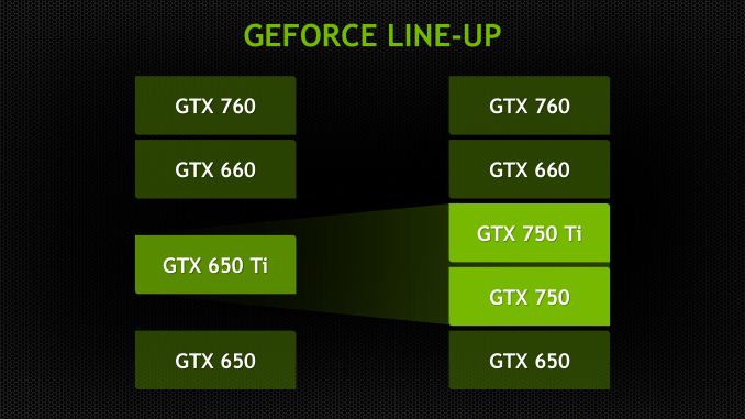
NVIDIA's Product Positioning
With up to 640 CUDA cores that hit above their weight and a TDP below 75W, GTX 750 Ti and GTX 750 will be filling a duo of roles in the NVIDIA lineup. From a performance and price standpoint NVIDIA is placing them between the GK106 flagship GTX 660 and the GK107 flagship GTX 650. GTX 750 Ti isn’t quite fast enough to displace GTX 660, so GTX 660 continues to live for another day while NVIDIA uses GTX 750 Ti to retire GTX 650 Ti Boost, and GTX 750 to retire GTX 650 Ti. Both of those were based on cut-down GK106 GPUs, so there’s an immediate benefit to NVIDIA of reducing production costs, and for consumers these new GTX 750 series cards will be faster than the cards they replace by roughly the same performance factor as we’ve seen elsewhere for GTX 700 series cards. Elsewhere GTX 650 and below will also live for another day as budget offerings, due to GK107’s smaller die size and lower production costs.
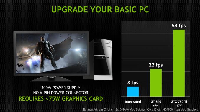
Meanwhile these sub-75W TDPs means that the GTX 750 series are now going to be NVIDIA’s best cards for the sub-75W PCIe bus powered only market. GTX 650, despite its TDP, required a 6pin PCIe power connector, so in that space the GTX 750 series is replacing the even slower GT 640 (GK107 + DDR3) as NVIDIA’s top card. For the purposes of the desktop video card space this puts the GTX 750 series squarely in the middle of the HTPC space and OEM upgrade space.
The HTPC space has long favored sub-75W cards for noise and space reasons, and NVIDIA’s video decode power improvements should be further welcome in this space. In this sense NVIDIA’s petite products for smaller form factor computers will be an interesting split between the reference GTX 780 and the GTX 750 series. Reference GTX 780 being well suited for small form factor designs due to its well-constructed blower, and the GTX 750 series being well suited for very low power designs or designs that don’t meet the air intake requirements for a blower.
As for the OEM upgrade space, this is a fairly straightforward but large market. The two sweet spots for video card upgrades for OEM systems are sub-150W cards for the OEMs that supply a single PCIe power plug (some of them), and sub-75W cards for OEMs that don’t supply a PCIe power plug, or even a very powerful PSU in the first place (more of them). These scenarios are fundamentally power limited – not unlike mobile – so having the fastest card at sub-150W and sub-75W is potentially very good for business. In NVIDIA’s case they are making a clear play for the sub-75W market with these cards, and one of their marketing pushes will be to go after OEM upgrades.
That said, whenever we’re talking about mainstream cards the Asia-Pacific (APAC) market becomes especially important due to its size and higher price sensitivity. Countries like China have been strong markets for cards like the GTX 750 series, so NVIDIA is expecting much of the same here. Once again NVIDIA’s strongest play will be the sub-75W market given their power advantage, as in unrestricted power scenarios AMD will have the upper hand. The wild card factor here will be APAC’s far greater use of internet cafes and LAN gaming centers, as operators are likely to be more interested in power consumption when it’s spread out over numerous computers.
Pricing & Competitive Landscape
Wrapping things up, the GTX 750 series will be a hard launch with immediate availability on a global scale. NVIDIA is placing the MSRP for the GTX 750 Ti at $149 and the MSRP for the GTX 750 at $119, right between the GTX 660 and GTX 650, while pushing GTX 650 Ti out of the picture entirely. From a performance perspective these cards won’t offer the kind of performance that will entice most 600 series owners to upgrade (though the performance gains against GT 640 are striking), but NVIDIA is making a major effort to target GTX 550 Ti and GTS 450 owners as those cards turn 3-4 years old, with the GTX 750 series able to easily double their performance while reducing power consumption.
AMD’s competition for the GTX 750 series will be the recently launched Radeon R7 265, and the recently price dropped Radeon R7 260X, which are set to go for $149 and $119 respectively. Unfortunately R7 265 was not a hard launch and is not expected until the end of this month, so NVIDIA is going to have roughly two weeks of availability ahead of AMD at $149, and meanwhile at $119 we’re still waiting to see the announced price cuts take effect.
From a price/performance standpoint NVIDIA is not going to be especially competitive, and this is similar to how NVIDIA handled the mainstream cards in the 600 series. NVIDIA is content to take second place on a price/performance basis, relying on their stronger brand name and greater brick & mortar retail presence to make up for what they lose from lower performance, a strategy that apparently worked well for the 600 series. Accordingly, once they hit the market (and assuming they stay at MSRP), R7 265 and R7 260X will be faster than their GTX 750 series’ counterparts, as AMD is just outright throwing more hardware at the problem. But as a result AMD will not be able to compete with NVIDIA’s power efficiency; in those sub-75W markets NVIDIA will have the more powerful (and more expensive) options.
| Winter 2014 GPU Pricing Comparison | |||||
| AMD | Price | NVIDIA | |||
| Radeon R9 270 | $250 | GeForce GTX 760 | |||
| $190 | GeForce GTX 660 | ||||
| Radeon R7 265 | $150 | GeForce GTX 750 Ti | |||
| Radeon R7 260 | $130 | ||||
| Radeon R7 260X (New MSRP) | $120 | GeForce GTX 750 | |||
| Radeon R7 250X | $100 | GeForce GTX 650 | |||
| Radeon R7 250 | $90 | GeForce GT 640 | |||
Meet The Reference GTX 750 Ti & Zotac GTX 750 Series
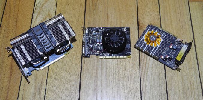
For the launch of the GTX 750 series NVIDIA is doing a pure virtual launch. NVIDIA’s partners will be launching with custom cards from day-one, and while NVIDIA has put together a reference board for testing and validation purposes, the partners will not be selling that reference board. Instead we’ll be seeing semi-custom and fully-custom designs; everyone has their own cooler, a lot of partners will be using the NVIDIA reference PCB, and others will be rolling out their own PCBs too. Since these are sub-75W/sub-$150 cards there’s not a lot of room for variation – expect single and dual fan open air coolers – but we’ll have to see just what the partners cook up. GM107 should be suitable for fully passive designs and low-profile designs, and while we’ve seen one low-profile design so far we haven’t seen any passive designs yet.
Meanwhile for the purposes of the GTX 750 Ti launch NVIDIA has seeded the press with the GTX 750 Ti reference board for evaluation purposes. They have not seeded the press with GTX 750 boards, so we’ll be looking at a retail board in that scenario.
Reference GeForce GTX 750 Ti
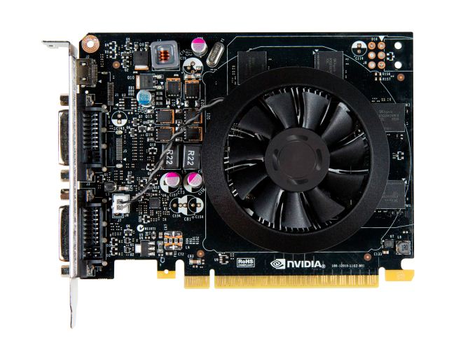
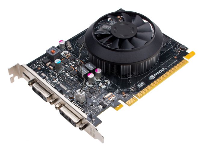
The reference GeForce GTX 750 Ti is fairly typical of what retail boards will be like. NVIDIA’s cooler of choice on the reference GTX 750 Ti is a small but effective open air double-wide cooler. NVIDIA’s using a low-profile aluminum heatsink that covers roughly half the card, topped with a 55mm fan. This is the cooler style that most partners will mimic, as the 60W TDP of the GTX 750 Ti does not require a particularly large cooler. As is common with open air coolers, the heatsink itself doesn’t make contact with the on-board RAM, so RAM cooling is left to airflow coming off of the fan.
NVIDIA’s RAM of choice for the GTX 750 Ti is their traditional favorite, Hynix 6GHz GDDR5, with NVIDIA using Hynix’s new 4Gb modules to get 2GB with just 4 modules. The use of 6GHz RAM, which will be common across this product, means that the GTX 750 Ti will have some memory overclocking headroom right out of the box, memory bus willing. NVIDIA uses 4 pieces of it in a 4x32bit configuration, with 4 more pads on the back of the card for another 4 pieces for 4GB cards should the need arise.
Moving on, the PCB itself is largely lifted from the GTX 650 and GTX 650 Ti, the similar TDPs allowing partners to get their customized cards out right away, and indicating that GM107 doesn’t have significantly different I/O or power delivery requirements than GK107. This puts the length of the card at 5.75” – about as short as a PCIe x16 card can be – in a full-profile form factor. There is a spot on the board for a PCIe power socket, and while it’s not used nor necessary on the reference design, this does leave the door open to more aggressive overclocking designs on partner cards.
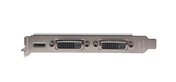
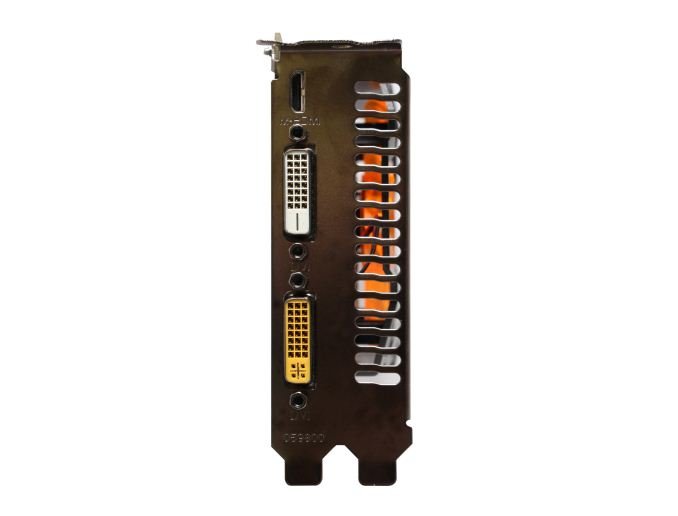
Finally, display connectivity is provided by 1 DL-DVI-I port, 1 DL-DVI-D port, and a mini-HDMI port. Since Maxwell GPUs support 4 displays the GTX 750 Ti can drive up to 3 displays via these connectors in any combination and configuration. The lack of a DisplayPort is disappointing, but not surprising. With most partners opting for 2x DVI and 1x mini-HDMI on their GTX 650 series cards, the PCB reuse means the GTX 750 Ti launch cards will be of a similar makeup. As a result we will see some DisplayPort enabled cards, and we wouldn’t be surprised if this shifted a bit over the coming months as partners move inventory and can take the time to do more customization to their designs. NVIDIA’s G-Sync technology would be a good match for these cards given the lower framerates we typically see, so having DisplayPort connectivity here will be important for NVIDIA’s G-Sync initiative as the first native G-Sync monitors hit the market later this year.
Zotac GeForce GTX 750 Series
| GeForce GTX 750 Series Specification Comparison | |||||
| GeForce GTX 750 Ti (Ref) | Zotac GeForce GTX 750 Ti | Zotac GeForce GTX 750 | |||
| Base Clock | 1020MHz | 1033MHz | 1033MHz | ||
| Boost Clock | 1085MHz | 1098MHz | 1098MHz | ||
| Memory Clock | 5.4GHz | 5.4GHz | 5.0GHz | ||
| VRAM | 2GB | 2GB | 1GB | ||
| TDP | 60W | 60W | 55W | ||
| Width | Double Slot | Double Slot | Double Slot | ||
| Length | 5.75" | 6" | 6" | ||
| Warranty | N/A | 3 Year (Upon Registration) | 3 Year (Upon Registration) | ||
| Price | $149 | $149 | $119 | ||
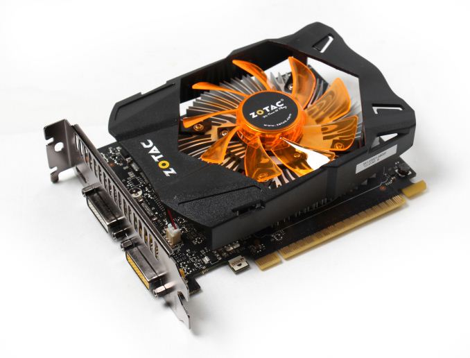
For retail cards we were able to get our hands on Zotac’s entry level GeForce GTX 750 series cards. As both of these cards use the same PCB and cooler, we’ll be referring to them together unless otherwise noted.
As is often the case, Zotac’s entry level GeForce GTX 750 series cards end up being very similar to the NVIDIA reference design. The PCB as far as we can tell is identical to the reference PCB, so all of the power delivery and clockspeed properties are the same.
Zotac’s cooler of choice is lifted from their GTX 650 Ti, and like NVIDIA’s reference design is an open air cooler. Zotac is using an 85mm fan suspended over a mid-profile aluminum heatsink that covers just over half the card, with a minimal shroud around it. The heatsink only makes contact with the GPU, so cooling for the RAM and VRM components is supplied via airflow alone. The similarity between the Zotac and NVIDIA designs means that it has the same double-slot width, while the shroud pushes the length of the card out to 6” flat.
Meanwhile from a specification point of view Zotac has goosed their entry level cards slightly. Both cards start at one boost bin above NVIDIA’s reference, putting them at 1033MHz for the core clock as opposed to 1020MHz for a reference card. Zotac has not changed the RAM specifications however, so we’re still looking at 5.4GHz for GTX 750 Ti and 5.0GHz for GTX 750.
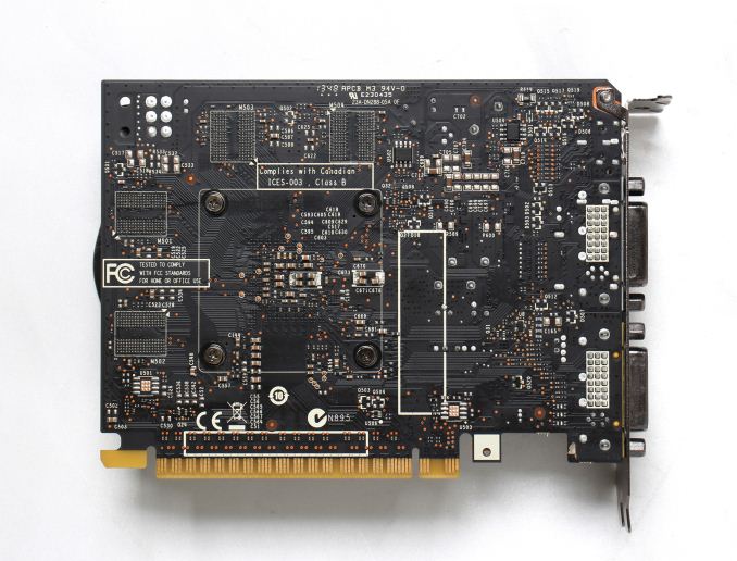 Speaking of RAM, looking at the Zotac GTX 750 we can get an idea of what to expect for RAM on a GTX 750 card. Zotac is using a 4x32bit configuration of Hynix H5GC2H24BFR-T2C, an interesting 2Gb module that can run at either 6GHz at normal voltages (1.5v), or 5GHz at low voltages (1.35v). We’re not able to tell which voltage mode Zotac is using, but given the configuration we wouldn’t be surprised to see them using 1.35v for extra power savings. Otherwise this means that the RAM on this card is significantly overpowered, which would be good for memory overclocking.
Meanwhile since Zotac’s PCB is identical to NVIDIA’s reference PCB, the I/O options are also the same: 1 DL-DVI-I port, 1 DL-DVI-D port, and a mini-HDMI port. Zotac tells us that they will also be releasing an OC edition card alongside these entry level cards, and that OC card will have a DisplayPort in order to be G-Sync ready.
Rounding out the package is the usual collection of a DVI-to-VGA adapter, Zotac’s “Boost Premium” OEM trialware, and the obligatory quickstart guides. Since these are entry level cards Zotac is sticking to NVIDIA’s MSRPs, putting their GTX 750 Ti card at $149 and their GTX 750 card at $119. Meanwhile for the warranty Zotac is offering a base 2 year warranty, which can be extended to a 3 year warranty by registering the card within 30 days.
HTPC Aspects : Introduction
Home Theater PC (HTPC) enthusiasts keep close tabs on launch of discrete GPUs which don't need a PCIe power connector. Such cards make it easy to upgrade an old PC with a low-wattage PSU into a multimedia powerhouse. Over the last decade or so, GPUs have implemented HTPC functionalities in response to consumer demand as well as changing / expected market trends. In the beginning, we had hardware acceleration for decode of MPEG-2. This was followed by H.264 / VC-1 acceleration (thanks to the emergence of Blu-rays), HD audio bitstreaming and 3D video support. More recently, we had support for playback and decode of videos in 4K resolution.
4K presents tangible benefits to consumers (unlike 3D), and market adoption is rapidly growing. In many respects, this is similar to how people migrated to 720p and 1080i TV sets when vendors started promoting high definition (HD). We know that these early adopters were stuck with expensive CRT-based TVs when the LCD-based 1080p sets came to the market at very reasonable prices. While there is no 'CRT-to-LCD'-like sea-change in the horizon, the imminent launch of HDMI '2.0' (The HDMI consortium wants to do away with version numbers for reasons known only to them) with 4Kp60 capability and display sinks fully compliant with that standard needs to be kept in mind by end users.
In the near future, it is expected that most of the 4K material reaching consumers will be encoded in H.264. Consumer devices such as the GoPro cameras still record 4K in that codec only. From a HTPC GPU perspective, it is imperative that we have support for 4K H.264 decoding. In fact, most real-time encoding activities would utilize H.264, but, a good HEVC (H.265) encoder would definitely be more efficient in terms of bitrate. The problem is that it is very difficult to make a good HEVC encoder operate in real-time. Archiving content wouldn't be a problem, though. So, it can be expected that content from streaming services / local backup (where the encoding is done offline) will move to HEVC first. A future-proof HTPC GPU would be capable of HEVC decode too.
Where does the Maxwell-based 750Ti stand when the above factors are taken into account? Make no mistake, the NVIDIA GT 640 happens to be our favourite HTPC GPU when 4K-capability is considered an absolute necessity. On paper, the 750Ti appears to be a great candidate to take over the reins from the GT 640. In order to evaluate the HTPC credentials, we put the 750Ti to test against the Zotac GT 640 as well as the Sapphire Radeon HD 7750.
In our HTPC coverage, we first look at GPU support for network streaming services, followed by hardware decoder performance for local file playback. This section also covers madVR. In the third section, we take a look some of the miscellaneous HTPC aspects such as refresh rate accuracy and hardware encoder performance.
The HTPC credentials of the cards were evaluated using the following testbed configuration:
| NVIDIA GT 750Ti HTPC Testbed Setup | |
| Processor / GPU | Intel Core i7-3770K - 3.50 GHz (Turbo to 3.9 GHz) |
| NVIDIA GT 750Ti / Zotac GT 640 / Sapphire Radeon HD 7750 | |
| Motherboard | Asus P8H77-M Pro uATX |
| OS Drive | Seagate Barracuda XT 2 TB |
| Secondary Drive | OCZ Vertex 2 60 GB SSD + Corsair P3 128 GB SSD |
| Memory | G.SKILL ECO Series 4GB (2 x 2GB) SDRAM DDR3 1333 (PC3 10666) F3-10666CL7D-4GBECO CAS 9-9-9-24 |
| Case | Antec VERIS Fusion Remote Max |
| Power Supply | Antec TruePower New TP-550 550W |
| Operating System | Windows 8.1 Pro |
| Display / AVR | |
| Sony KDL46EX720 + Pioneer Elite VSX-32 | |
| Acer H243H | |
| Graphics Drivers | GeForce v334.69 / Catalyst 14.1 Beta |
| Softwares | CyberLink PowerDVD 13 |
| MPC-HC 1.7.3 | |
| madVR 0.87.4 | |
All the three cards were evaluated using the same hardware and software configuration. The Sapphire Radeon HD 7750 has an advantage in the power consumption department thanks to its passive cooling system. Other than that, we are doing apples-to-apples comparison when talking about power consumption numbers for various activities in the next few sections.
HTPC Aspects : Network Streaming Performance
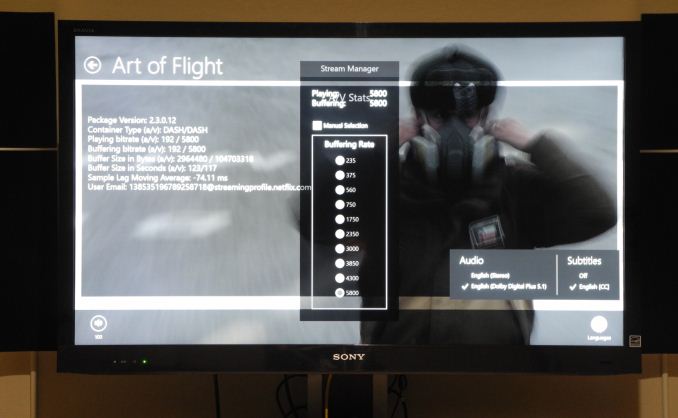
Windows 7-based HTPCs need hardware acceleration in both Adobe Flash and Microsoft Silverlight for optimal streaming performance with YouTube and Netflix. The move to Windows 8.1 has made Silverlight unnecessary. The Netflix app on Windows 8.x brings a HTPC's capability on par with dedicated streaming consoles, with support for Super HD (6 Mbps) streams as well as Dolby Digital Plus bitstreaming support. The latest app also renders the video in such a way as to make taking screenshots an exercise in frustration.
As the above photograph shows, the Netflix app can be set to bitstream Dolby Digital Plus to the AV receiver and the 750Ti supports it. The video and audio streams are at 5.8 Mbps and 192 kbps respectively. It is not immediately evident as to whether GPU acceleration is being utilized. However, tracking the GPU / VPU loading and PC power consumption numbers make it obvious that it is not software decode at work in the Netflix app.
Unlike Silverlight, Adobe Flash continues to maintain some relevance right now. YouTube continues to use Adobe Flash to serve FLV (at SD resolutions) and MP4 (at both SD and HD resolutions) streams. YouTube's debug OSD indicates whether hardware acceleration is being used or not.
Similar to our Netflix streaming test, we recorded GPU / VPU loading as well as power consumption at the wall when streaming the 1080p version of the sample YouTube clip. The table below presents the relevant numbers for various configurations and streaming services.
| Streaming Video Performance | ||||||
| Netflix | YouTube | |||||
| GPU/VPU Load | Power | GPU/VPU Load | Power | |||
| NVIDIA GeForce GTX 750 Ti | 11.95/12.65% | 56.44 W | 16.26/15.74% | 55.45 W | ||
| NVIDIA GeForce GT 640 | 5.99/25.80% | 58.89 W | 15.57/25.72% | 58.93 W | ||
| AMD Radeon HD 7750 | 0.72% | 66.79 W | 3.57% | 67.11 W | ||
NVIDIA has been touting Maxwell's low power nature, and it proves to be the best of the three candidates in terms of power efficiency when it comes to GPU support for streaming services.
HTPC Aspects : Decoding & Rendering Benchmarks
Our decoding and rendering benchmarks consists of standardized test clips (varying codecs, resolutions and frame rates) being played back through MPC-HC v1.7.3 (which comes with LAV Filters 0.60.1.5 in-built). GPU usage is tracked through GPU-Z logs and power consumption at the wall is also reported. The former provides hints on whether frame drops could occur, while the latter is an indicator of the efficiency of the platform for the most common HTPC task - video playback. Starting with this review, we have added two new streams to our benchmark suite. The first one is a 1080p24 H.264 clip (the type of content that most HTPC users watch), while the second one is a 2160p30 (4Kp30) H.264 clip (which will give us a way to test the downscaling performance of various codec / renderer combinations).
In the course of our testing, we found that our standard 1080p60 H.264 clip played with lots of artifacts on the GT 750Ti. This happened with both MPC-HC and CyberLink PowerDVD13. Using the same drivers on the GT 640 resulted in perfect playback. [Update: NVIDIA got back to us indicating that this is a Maxwell-related driver issue. We are waiting for new drivers]
It will be interesting to determine the reason behind this issue. Not all 1080p60 clips had this problem, though. On the positive side, both the GT 750Ti and the GT 640 (as expected) were able to decode UHD / 4K streams using the GPU. The 7750 fell back to software decode (avcodec) for those streams despite the relevant setting being ticked in the LAV Video Decoder configuration.
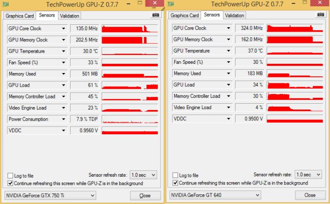
Before proceeding to the renderer benchmark numbers, it is important to explain the GPU loading numbers in the tables below. It goes without saying that the GPU loading of NVIDIA cards must obviously not be compared directly to the AMD card. Even amongst the NVIDIA cards, the loading numbers don't signify the same thing. The GPU load numbers reported by GPU-Z don't take into consideration the core clock. Maxwell GPUs have more fine-grained clock control. For example, when playing back 4Kp30 material, the 750 Ti's core clock is around 824 MHz, but, when playing 1080p24 material, it scales down to 135 MHz. Kepler, on the other hand, seems to use 824 MHz when playing back both 4Kp30 and 1080p24 material. For 480i, it goes down to 324 MHz. In terms of GPU loading on the GTX 750 Ti, we find 4Kp30 playback reporting a load of 2.65%, while 1080p60 reports 46% under EVR. The 2% loading is under much higher core clocks compared to the clock being used for 1080p60 playback. For the GT 640, this 'disconnect' is much harder to observe, since the clocks are same for most HD material. However, in the GT 640 segment of the screenshot below, it is possible to observe a higher GPU load of 34% for 480i60 material (the third part) compared to a lower value at higher clocks for 1080p24 material.
GPU-Z 0.7.7 Sensor Readings - Fine-grained clock control in Maxwell (4Kp30 and 1080p24 playback) compared to Kepler (4Kp30, 1080p24 and 480i60 playback). Core-clock / Load numbers 'disconnect' can be observed in both cases for Maxwell, but only in the 480i60 case for Kepler.
In any case, if the GPU usage is hovering above 95%, it is likely that the playback suffered from dropped frames. In terms of apples-to-apples comparison for efficiency purposes, the power consumption at the wall reigns supreme.
Enhanced Video Renderer (EVR)
The Enhanced Video Renderer is the default renderer made available by Windows 8.1. It is a lean renderer in terms of usage of system resources since most of the aspects are offloaded to the GPU drivers directly. EVR is mostly used in conjunction with native DXVA2 decoding. The GPU is not taxed much by the EVR despite hardware decoding also taking place. In our evaluation, all video post processing steps were left for MPC-HC to decide (except for the explicit activation of inverse telecine). In all our tests, we used the native DXVA2 decoder provided by MPC-HC's internal LAV Video Decoder. Deinterlacing mode was set to aggressive in the LAV Video Decoder setting. The GT 750Ti's VPU loading barely went above 40% even when decoding 1080p60 or 4Kp30 clips.
| Enhanced Video Renderer (EVR) Performance | ||||||
| Stream | GTX 750 Ti | GT 640 | HD 7750 | |||
| GPU Load (%) | Power | GPU Load (%) | Power | GPU Load (%) | Power | |
| 480i60 MPEG2 | 44.67 | 57.15 W | 20.92 | 68.74 W | 14.76 | 68.42 W |
| 576i50 H264 | 55.57 | 57.25 W | 19.28 | 69.37 W | 12.16 | 69.01 W |
| 720p60 H264 | 38.91 | 56.75 W | 36.05 | 61.08 W | 9.90 | 68.16 W |
| 1080i60 MPEG2 | 80.92 | 59.53 W | 32.76 | 71.27 W | 15.06 | 69.03 W |
| 1080i60 H264 | 55.87 | 63.34 W | 35.79 | 73.11 W | 18.78 | 71.21 W |
| 1080i60 VC1 | 79.29 | 60.69 W | 35.07 | 72.63 W | 18.91 | 70.97 W |
| 1080p60 H264 | 45.53 | 57.67 W | 39.29 | 61.91 W | 11.87 | 69.02 W |
| 1080p24 H264 | 15.69 | 55.06 W | 15.61 | 58.26 W | 4.62 | 67.47 W |
| 4Kp30 H264 | 2.65 | 63.89 W | 24.21 | 67.33 W | 11.36 | 76.90 W |
Enhanced Video Renderer - Custom Presenter (EVR-CP)
EVR-CP is the default renderer used by MPC-HC. It is slightly more resource intensive compared to EVR, as some explicit post processing steps are done on the GPU without going through DXVA post processing API calls provided by the driver.
| Enhanced Video Renderer - Custom Presenter (EVR-CP) Performance | ||||||
| Stream | GTX 750 Ti | GT 640 | HD 7750 | |||
| GPU Load (%) | Power | GPU Load (%) | Power | GPU Load (%) | Power | |
| 480i60 MPEG2 | 61.58 | 58.99 W | 18.97 | 69.22 W | 11.99 | 69.93 W |
| 576i50 H264 | 55.45 | 57.93 W | 17.97 | 68.81 W | 9.93 | 69.85 W |
| 720p60 H264 | 54.18 | 58.88 W | 47.97 | 63.17 W | 12.54 | 70.93 W |
| 1080i60 MPEG2 | 17.69 | 68.38 W | 39.84 | 73.85 W | 22.82 | 72.01 W |
| 1080i60 H264 | 16.92 | 70.14 W | 42.62 | 74.35 W | 21.97 | 73.43 W |
| 1080i60 VC1 | 17.45 | 69.77 W | 41.79 | 73.99 W | 22.03 | 73.56 W |
| 1080p60 H264 | 56.5 | 60.07 W | 19.80 | 70.64 W | 13.36 | 71.61 W |
| 1080p24 H264 | 25.61 | 56.83 W | 23.80 | 60.36 W | 9.68 | 69.20 W |
| 4Kp30 H264 | 5.52 | 67.11 W | 27.51 | 70.76 W | 26.10 | 84.03 W |
Experimenting with madVR
madVR provides plenty of options to tweak. For our evaluation, we considered two main scenarios. Our first run was with the default settings ( Chroma upscaling: Bicubic with Sharpness 75, Image upscaling: Lanczos 3-tap and Image downscaling: Catmull-Rom). With these settings, both the GT 640 and 750Ti processed all our test clips without dropping frames. The HD 7750 failed with the 720p60 and 1080p60 clips.
| madVR (Default Settings) Performance | ||||||
| Stream | GTX 750 Ti | GT 640 | HD 7750 | |||
| GPU Load (%) | Power | GPU Load (%) | Power | GPU Load (%) | Power | |
| 480i60 MPEG2 | 76.02 | 62.27 W | 28.77 | 73.68 W | 20.91 | 74.76 W |
| 576i50 H264 | 73.21 | 62.10 W | 30.93 | 74.24 W | 20.88 | 75.40 W |
| 720p60 H264 | 19.34 | 69.89 W | 35.18 | 75.42 W | 25.11 | 78.46 W |
| 1080i60 MPEG2 | 23.16 | 71.08 W | 49.53 | 77.78 W | 27.74 | 78.22 W |
| 1080i60 H264 | 24.87 | 71.79 W | 52.27 | 78.26 W | 28.13 | 79.67 W |
| 1080i60 VC1 | 24.47 | 71.06 W | 51.48 | 77.74 W | 27.88 | 79.18 W |
| 1080p60 H264 | 20.49 | 70.43 W | 42.30 | 76.45 W | 29.72 | 79.16 W |
| 1080p24 H264 | 41.70 | 59.20 W | 43.98 | 63.41 W | 14.03 | 72.08 W |
| 4Kp30 H264 | 27.51 | 73.24 W | 66.72 | 81.54 W | 23.06 | 100.94 W |
The second run was with our stress settings (Chroma and image upscaling : Jinc 3-tap with anti-ringing filter activated, Image downscaling : Lanczos 3-tap with anti-ringing filter activated). With these settings, the GT 750Ti was able to process all test clips without dropping frames. However, the GT 640 failed the 576i50 / 720p60 / 1080i60 / 4Kp30 clips. The HD 7750 failed the 720p60, 1080p60 and 4Kp30 clips.
| madVR (Stress Settings) Performance | ||||||
| Stream | GTX 750 Ti | GT 640 | HD 7750 | |||
| GPU Load (%) | Power | GPU Load (%) | Power | GPU Load (%) | Power | |
| 480i60 MPEG2 | 50.53 | 76.35 W | 90.48 | 88.77 W | 70.38 | 89.99 W |
| 576i50 H264 | 55.08 | 76.92 W | 95.09 | 92.75 W | 80.21 | 91.65 W |
| 720p60 H264 | 63.65 | 84.37 W | 96.82 | 93.72 W | 92.64 | 95.85 W |
| 1080i60 MPEG2 | 51.29 | 76.43 W | 95.93 | 89.86 W | 63.32 | 88.58 W |
| 1080i60 H264 | 52.65 | 77.06 W | 94.9 | 90.63 W | 64.26 | 89.64 W |
| 1080i60 VC1 | 51.71 | 77.33 W | 96.86 | 90.31 W | 64.28 | 89.09 W |
| 1080p60 H264 | 54.43 | 77.92 W | 96.63 | 91.71 W | 73.20 | 92.09 W |
| 1080p24 H264 | 76.58 | 62.23 W | 38.04 | 75.26 W | 24.82 | 77.68 W |
| 4Kp30 H264 | 77.52 | 99.33 W | 99 | 101.13 W | 95.71 | 117.07 W |
As entry level HTPC GPUs become more and more powerful, madVR keeps pushing the bar higher too. Recently, NNEDI3 was added as an upscaling algorithm option. In our experiments with a 1080p display output, NNEDI3 and Jinc 3-tap (for chroma and luma upscaling) work for 1080p24 or lower resolution / frame rate clips in the 750Ti and 7750, but not in the GT 640. With NNEDI3, the NVIDIA driver is a bit buggy, with a greenish tinge all through. Any higher resolution / frame rate immediately chokes. Jinc 3-taps works fine, though. 4K to 1080p downscaling results in greenish screens intermittently, finally ending up with a resetting Direct 3D Device failure. The downscaling path seems to be buggy, either due to driver issues or bugs in madVR v0.87.4.
HTPC Aspects : Miscellaneous Factors
In this section, we cover some miscellaneous HTPC aspects that are too short to warrant a separate section. These include a discussion of various display refresh rates supported, a short look at the hardware encoder (NVENC) in action and a summary of our thoughts on the GT 750Ti as a HTPC GPU.
Refresh Rate Accuracy:
NVIDIA provides an easy way to customize refresh rates. The process remains the same as what we explained in our review of the GT 640. The 23 Hz setting gives us a refresh rate of 23.971 Hz. With Intel providing rock-solid 23.976 Hz support in Haswell, it is time NVIDIA got the out-of-the-box refresh rate support correct.
NVIDIA also allows setting of refresh rates not reported as available by the display's EDID. On the Sony KDL46EX720, it allowed driving of 1080p50 without any issues. The flexibility is definitely appreciated, though it would be nice to have better accuracy without all the tweaking.
Hardware Encoder: NVENC
We used CyberLink MediaEspresso v6.7 to evaluate the hardware encoder block. Our test clip was a 3-minute long 1080p24 H.264 stream at 36 Mbps and the target was a 720p24 H.264 stream at 6 Mbps. The time taken for conversion and the power consumption at the wall during the conversion process are provided in the table below.
| GPU Video Encoding Performance | ||||||
| Conversion Time | Power | |||||
| NVIDIA GeForce GTX 750 Ti | 2:54 | 88.97W | ||||
| NVIDIA GeForce GT 640 | 0:36 | 108.18W | ||||
| AMD Radeon HD 7750 (VCE) | 1:06 | 76.84W | ||||
| Intel HD 4000 QuickSync (Better Quality/Fast Conversion) | 0:24 | 63.91W | ||||
It appears as if the 750Ti is using the CUDA path rather than NVENC, while the 640 seems to use NVENC fine. We had readied ourselves for some quality comparison using objective metrics for the new NVENC. It looks like we have to wait for this issue to be resolved before proceeding down that path. [Update: NVIDIA got back to us indicating that this is a Maxwell-related driver issue. We are waiting for new drivers]
HTPC Verdict - Wait and Watch
We have taken a look at the HTPC credentials of the 750Ti and compared it with the GT 640 and the HD 7750. In terms of power efficiency, it is hard not to recommend the 750Ti. With a 60W TDP, it is amenable to passive cooling also. However, it comes to the market at a time when the HEVC standard has just been ratified (preventing it from having a full-blown hardware accelerated decoder) and HDMI 2.0 with 4Kp60 support being right around the corner. The perfect HTPC GPU would include support for both, but the 750Ti, unfortunately, is a bit early to the game. More troublesome is the fact that CyberLink's MediaEspresso seems unable to take advantage of the new NVENC and the fact that some of our 1080p60 H.264 clips are showing decoding artifacts (considering they play perfectly using the GT 640).
We would suggest HTPC enthusiasts to adopt a wait-and-watch approach to the GT 750Ti, particularly with respect to driver bugs specific to the 750Ti and also the extent of HEVC decode support that will be available. Depending on the requirements, it might also be prudent to wait for a Maxwell GPU with HDMI 2.0 support.
The Test
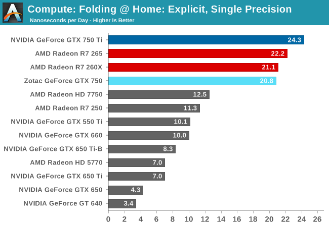
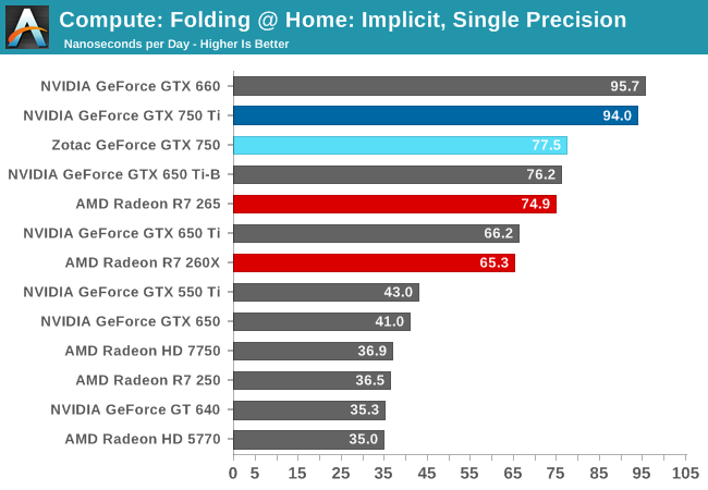
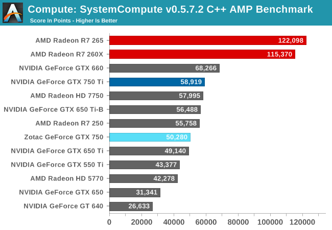
For this review we’re using the latest drivers from both NVIDIA and AMD. NVIDIA’s launch drivers are 334.69, which add support for the GTX 750 series but are otherwise identical to the 334.67 drivers currently available as a public beta for existing cards. The release 334 drivers include a fairly impressive tune up of NVIDIA’s OpenCL stack, so we’re finding that OpenCL performance is significantly improved in some of our benchmarks, which helps to close the gap with AMD. On the other hand these tune-ups have not come bug free (as Ganesh has found), and while our compute benchmarks are fine, Ganesh has run into some issues with some of his OpenCL based video utilities. Other than that, we have not encountered any stability problems with these drivers.
Meanwhile for AMD’s cards we’re using the recently released Catalyst 14.1 beta v1.6 drivers.
| CPU: | Intel Core i7-4960X @ 4.2GHz |
| Motherboard: | ASRock Fatal1ty X79 Professional |
| Power Supply: | Corsair AX1200i |
| Hard Disk: | Samsung SSD 840 EVO (750GB) |
| Memory: | G.Skill RipjawZ DDR3-1866 4 x 8GB (9-10-9-26) |
| Case: | NZXT Phantom 630 Windowed Edition |
| Monitor: | Asus PQ321 |
| Video Cards: |
NVIDIA GeForce GTX 750 Ti Zotac GeForce GTX 750 Ti Zotac GeForce GTX 750 NVIDIA GeForce GTX 660 NVIDIA GeForce GTX 650 Ti Boost NVIDIA GeForce GTX 650 Ti NVIDIA GeForce GTX 650 NVIDIA GeForce GTX 640 NVIIDA GeForce GTX 550 Ti AMD Radeon R7 265 AMD Radeon R7 260X AMD Radeon R7 250 AMD Radeon HD 7750 AMD Radeon HD 5770 |
| Video Drivers: |
NVIDIA Release 334.67 Beta NVIDIA Release 334.69 Beta (GTX 750 Series) AMD Catalyst 14.1 Beta v1.6 |
| OS: | Windows 8.1 Pro |
Metro: Last Light
As always, kicking off our look at performance is 4A Games’ latest entry in their Metro series of subterranean shooters, Metro: Last Light. The original Metro: 2033 was a graphically punishing game for its time and Metro: Last Light is in its own right too. On the other hand it scales well with resolution and quality settings, so it’s still playable on lower end hardware.
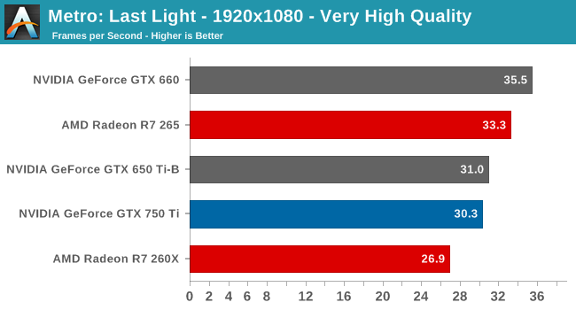
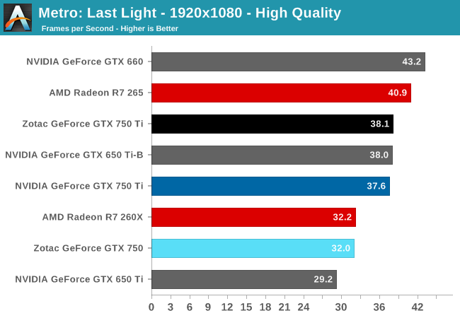
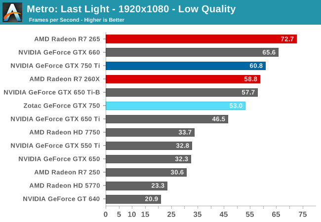
Diving into our performance analysis, we’ll be looking at a few different factors. On a competitive basis, the GTX 660 and the R7 265 are the GTX 750 Ti’s closest competitors. Though we’ll also want to compare it to GTX 650, so see what a GK107 versus GM107 matchup looks like. Meanwhile the GTX 750’s closest competitors will be the R7 260X, and to a lesser degree the GTX 650 Ti.
Being one of our more difficult games, Metro shows right off the bat that these mainstream video cards, no matter how fast they are, will face a difficult time. The GTX 750 Ti can stay comfortably above the 30fps at high quality, but the GTX 750 not so much.
What’s clear right off the bat two is two things. The first is that GTX 750 Ti, the GM107 flagship, is significantly faster than GTX 650, the GK107 flagship. GTX 750 Ti is just short of doubling GTX 650’s performance in this benchmark.
The second point is that neither GTX 750 series card is going to fare well against its AMD counterpart. Both the R7 265 and R7 260 are faster than the GeForce cards, and by over 10% at times.
Finally, GTX 750 Ti won’t be touching GTX 660 here. It’s close, but especially at higher quality settings the GTX 660 is pulling away. GTX 750 Ti can’t completely make up for the lack of memory bandwidth and ROP throughput.
Company of Heroes 2
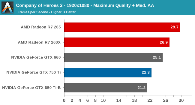
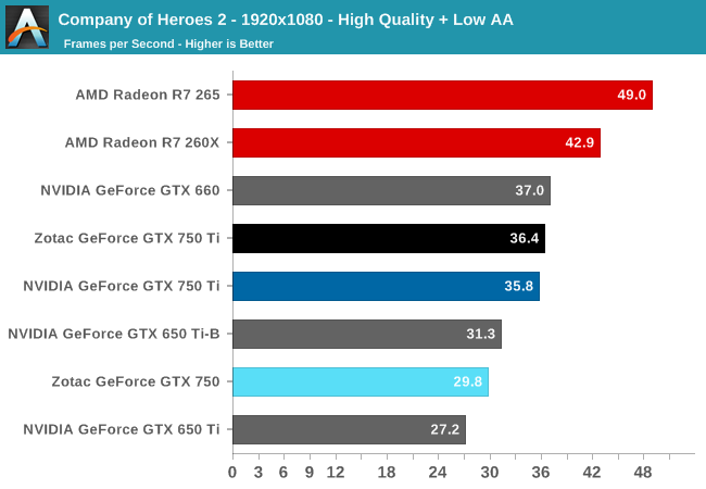
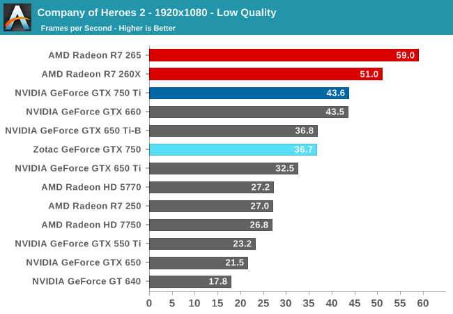
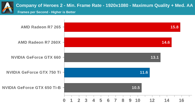
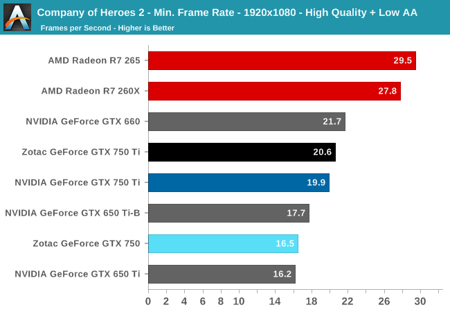
Our second benchmark in our benchmark suite is Relic Games’ Company of Heroes 2, the developer’s World War II Eastern Front themed RTS. For Company of Heroes 2 Relic was kind enough to put together a very strenuous built-in benchmark that was captured from one of the most demanding, snow-bound maps in the game, giving us a great look at CoH2’s performance at its worst. Consequently if a card can do well here then it should have no trouble throughout the rest of the game.

Bioshock Infinite
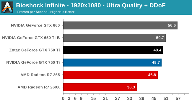
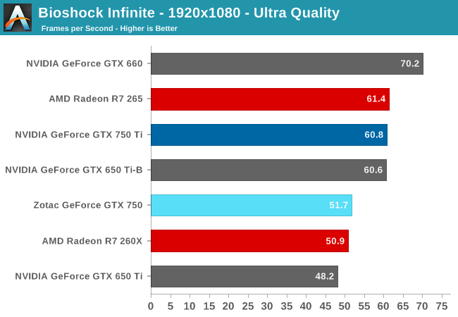
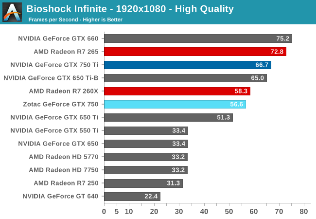
Bioshock Infinite is Irrational Games’ latest entry in the Bioshock franchise. Though it’s based on Unreal Engine 3 – making it our obligatory UE3 game – Irrational had added a number of effects that make the game rather GPU-intensive on its highest settings. As an added bonus it includes a built-in benchmark composed of several scenes, a rarity for UE3 engine games, so we can easily get a good representation of what Bioshock’s performance is like.
Battlefield 4
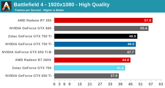
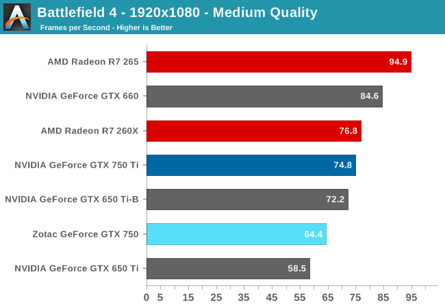
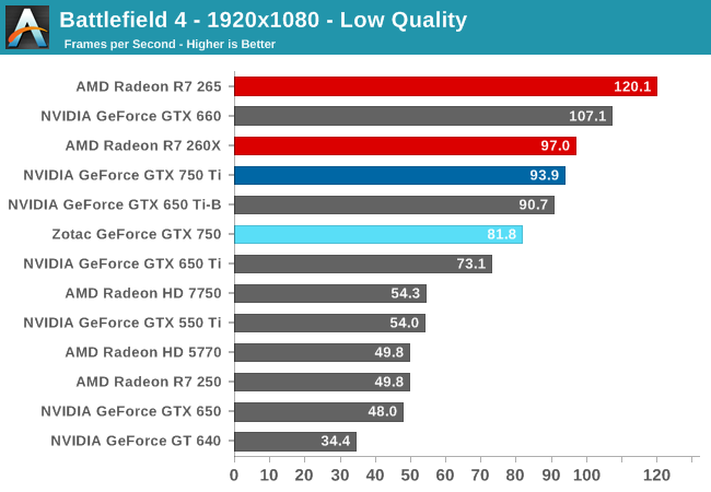
Our latest addition to our benchmark suite and our current major multiplayer action game of our benchmark suite is Battlefield 4, DICE’s 2013 multiplayer military shooter. After a rocky start, Battlefield 4 has finally reached a point where it’s stable enough for benchmark use, giving us the ability to profile one of the most popular and strenuous shooters out there. As these benchmarks are from single player mode, based on our experiences our rule of thumb here is that multiplayer framerates will dip to half our single player framerates, which means a card needs to be able to average at least 60fps if it’s to be able to hold up in multiplayer.
Crysis 3
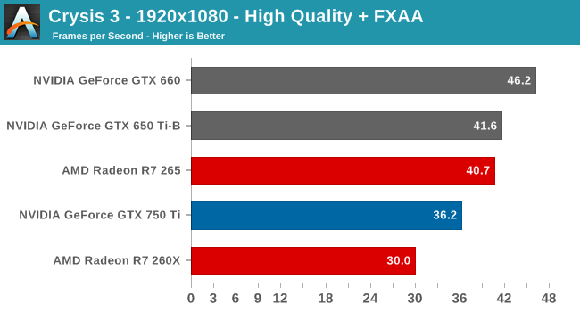
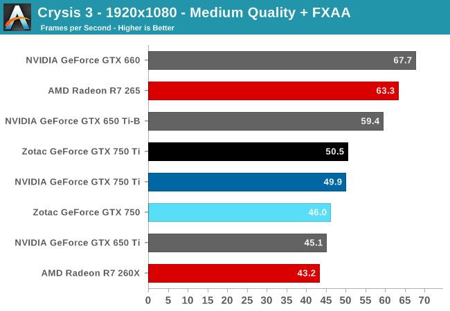
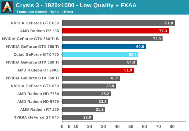
Still one of our most punishing benchmarks, Crysis 3 needs no introduction. With Crysis 3, Crytek has gone back to trying to kill computers and still holds “most punishing shooter” title in our benchmark suite. Only in a handful of setups can we even run Crysis 3 at its highest (Very High) settings, and that’s still without AA. Crysis 1 was an excellent template for the kind of performance required to drive games for the next few years, and Crysis 3 looks to be much the same for 2014.
Crysis: Warhead
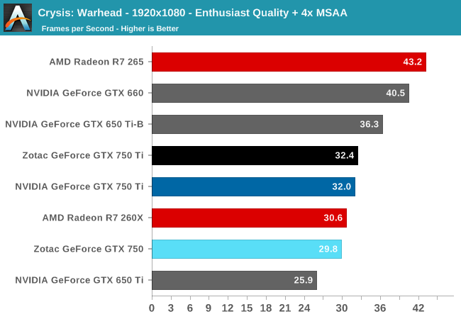
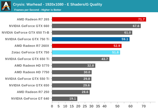
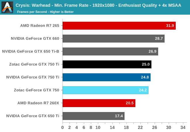
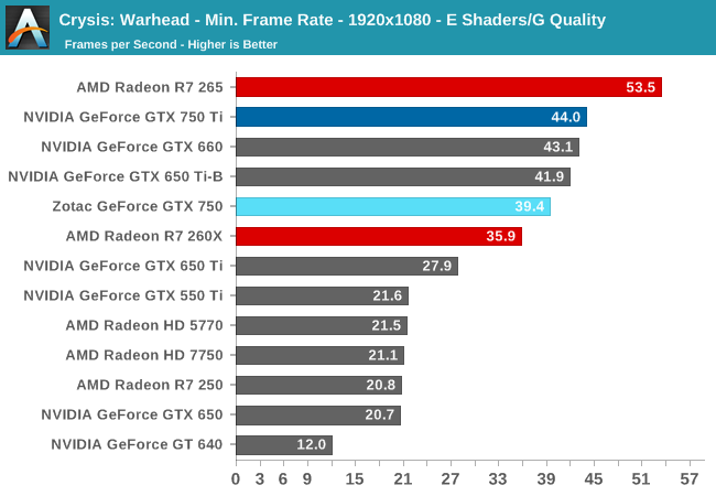
Up next is our legacy title for 2013/2014, Crysis: Warhead. The stand-alone expansion to 2007’s Crysis, at over 5 years old Crysis: Warhead can still beat most systems down. Crysis was intended to be future-looking as far as performance and visual quality goes, and it has clearly achieved that. We’ve only finally reached the point where single-GPU cards have come out that can hit 60fps at 1920 with 4xAA, never mind 2560 and beyond.
Total War: Rome 2
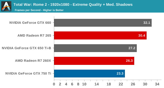
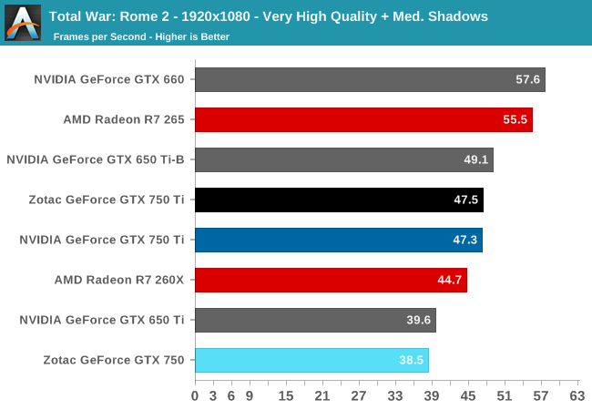
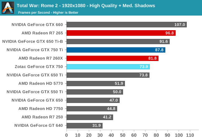
The second strategy game in our benchmark suite, Total War: Rome 2 is the latest game in the Total War franchise. Total War games have traditionally been a mix of CPU and GPU bottlenecks, so it takes a good system on both ends of the equation to do well here. In this case the game comes with a built-in benchmark that plays out over a forested area with a large number of units, definitely stressing the GPU in particular.
For this game in particular we’ve also gone and turned down the shadows to medium. Rome’s shadows are extremely CPU intensive (as opposed to GPU intensive), so this keeps us from CPU bottlenecking nearly as easily.
Hitman: Absolution
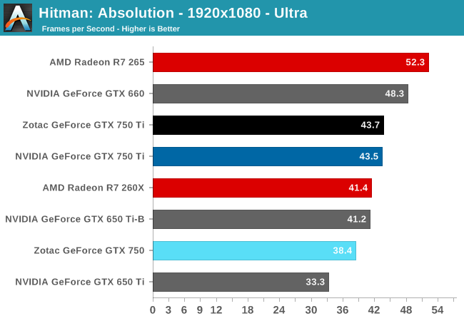
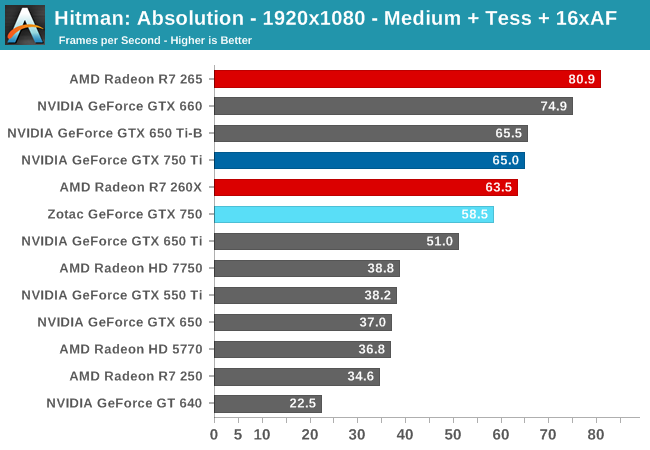
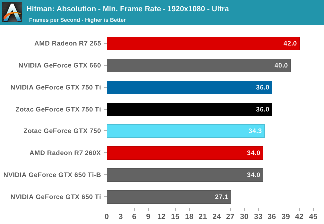
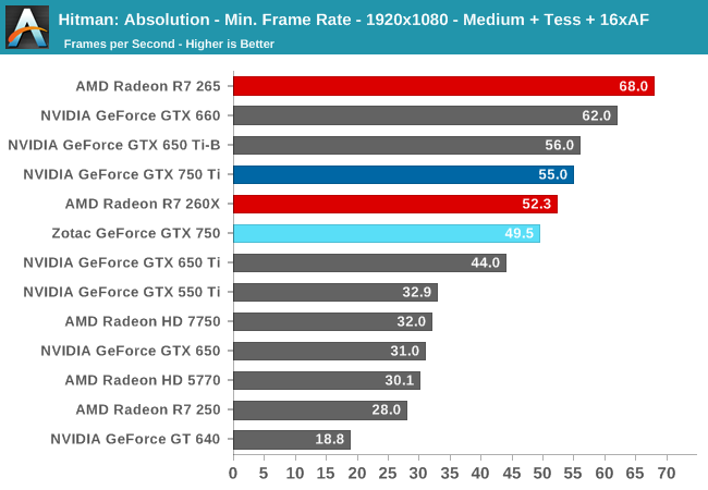
The second-to-last game in our lineup is Hitman: Absolution. The latest game in Square Enix’s stealth-action series, Hitman: Absolution is a DirectX 11 based title that though a bit heavy on the CPU, can give most GPUs a run for their money. Furthermore it has a built-in benchmark, which gives it a level of standardization that fewer and fewer benchmarks possess.
GRID 2
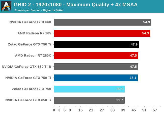
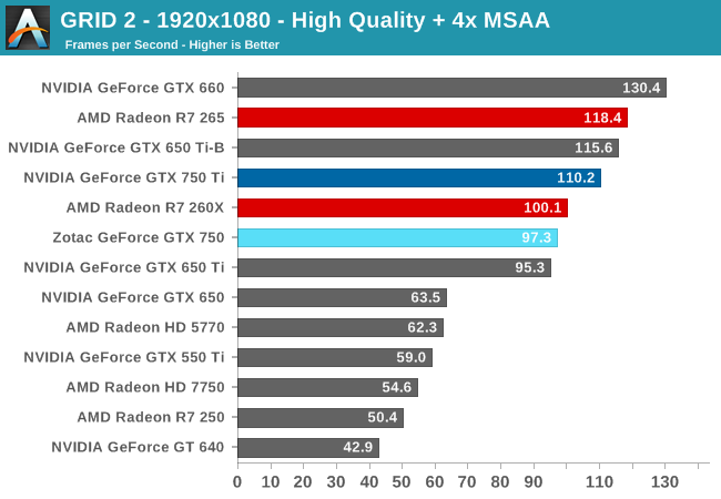
The final game in our benchmark suite is also our racing entry, Codemasters’ GRID 2. Codemasters continues to set the bar for graphical fidelity in racing games, and with GRID 2 they’ve gone back to racing on the pavement, bringing to life cities and highways alike. Based on their in-house EGO engine, GRID 2 includes a DirectCompute based advanced lighting system in its highest quality settings, which incurs a significant performance penalty but does a good job of emulating more realistic lighting within the game world.
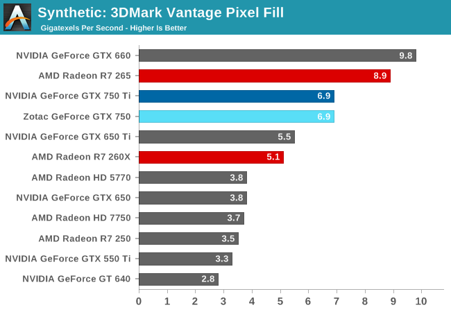
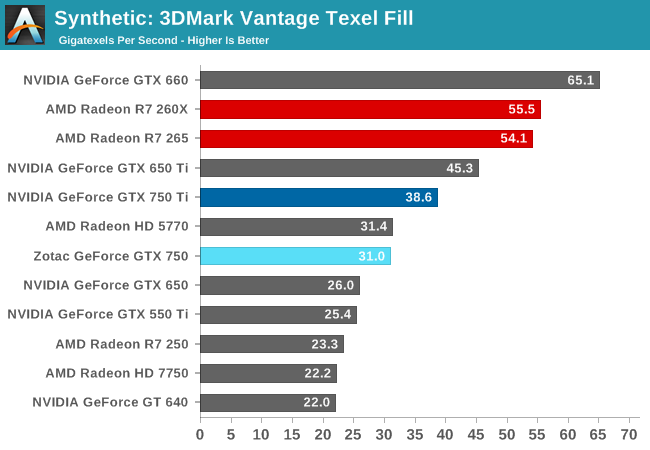
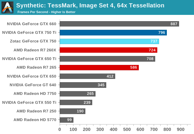
Synthetics
As always we’ll also take a quick look at synthetic performance.
Compute
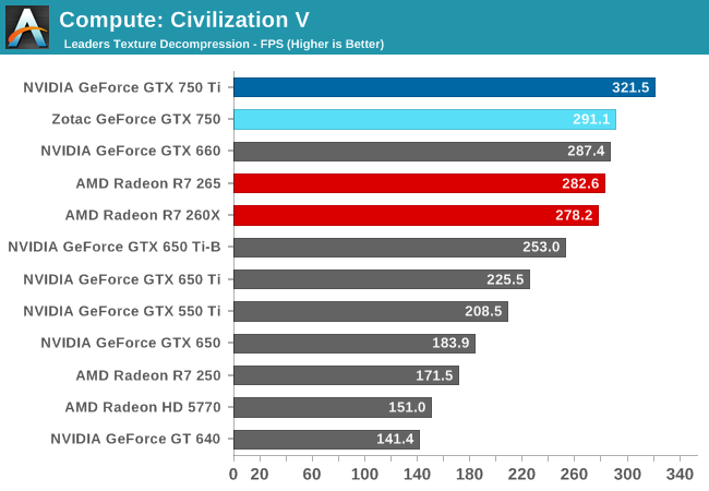
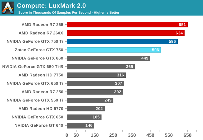
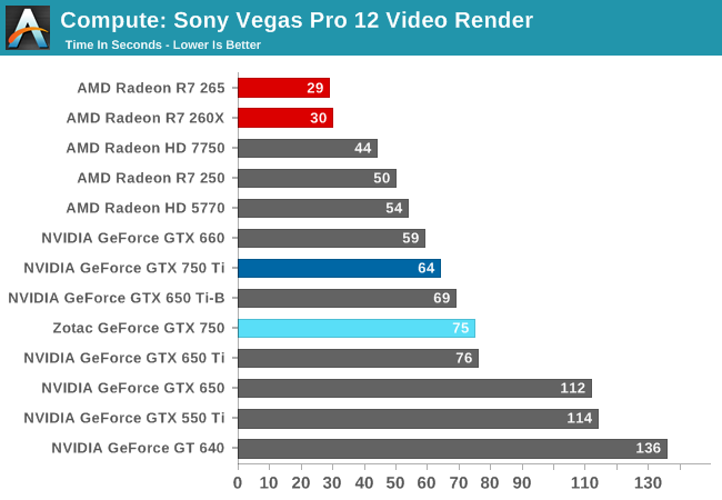
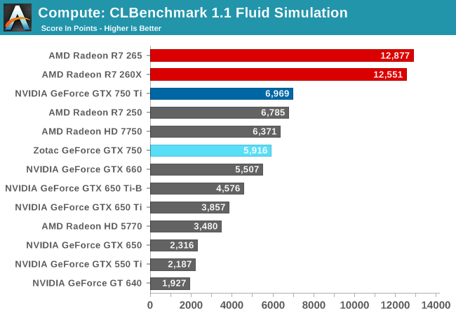
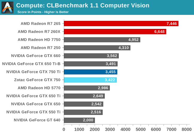
Jumping into compute
Power, Temperature, & Noise
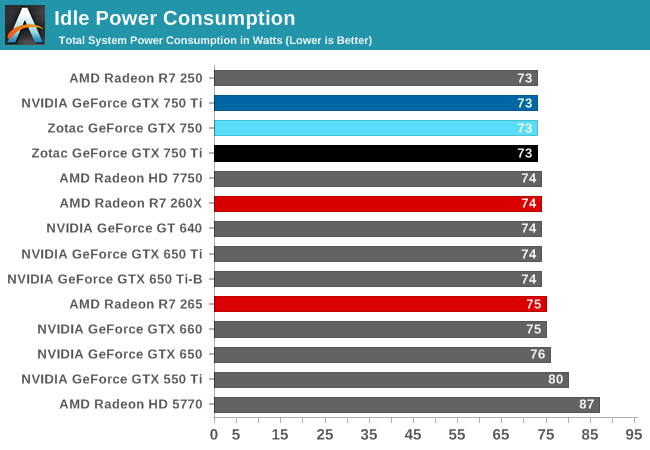
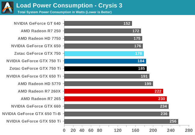
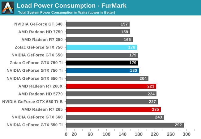
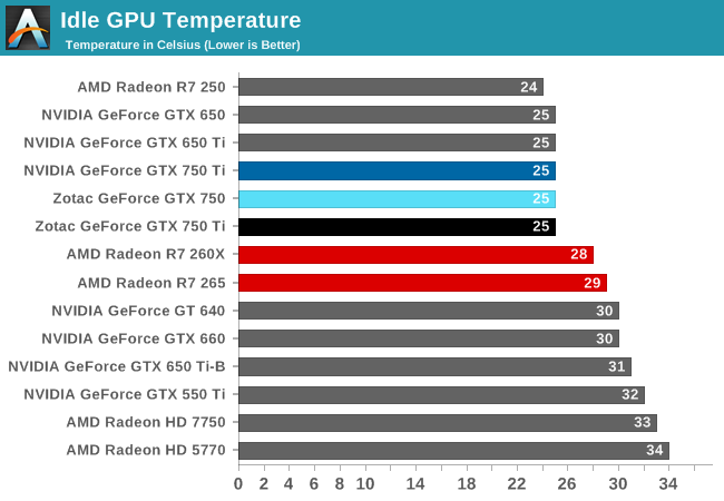
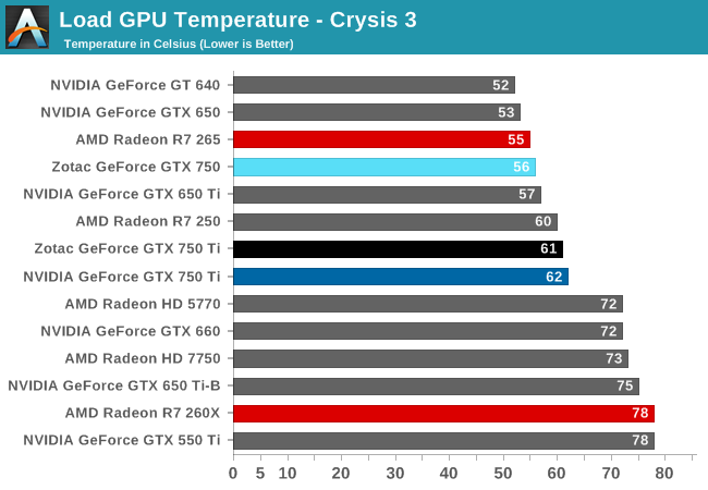
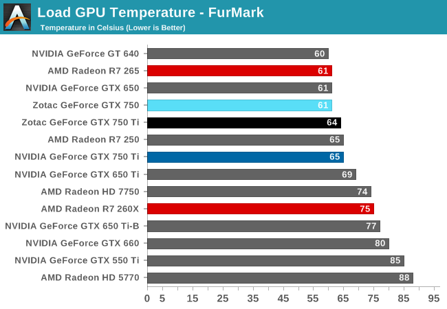
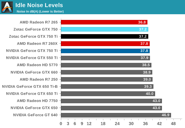
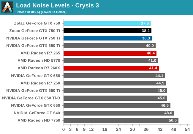
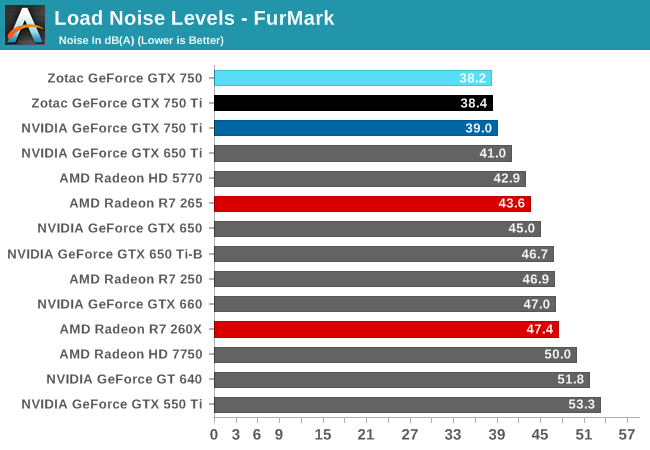
As always, last but not least is our look at power, temperature, and noise. Next to price and performance of course, these are some of the most important aspects of a GPU, due in large part to the impact of noise. All things considered, a loud card is undesirable unless there’s a sufficiently good reason – or sufficiently good performance – to ignore the noise.
| GeForce GTX 750 Series Voltages | ||||
| Ref GTX 750 Ti Boost Voltage | Zotac GTX 750 Ti Boost Voltage | Zotac GTX 750 Boost Voltage | ||
| 1.168v | 1.137v | 1.187v | ||
For those of you keeping track of voltages, you’ll find that the voltages for GM107 as used on the GTX 750 series is not significantly different from the voltages used on GK107. Since we’re looking at a chip that’s built on the same 28nm process as GK107, the voltages needed to drive it to hit the desired frequencies have not changed.
| GeForce GTX 750 Series Average Clockspeeds | |||||
| Ref GTX 750 Ti | Zotac GTX 750 Ti | Zotac GTX 750 | |||
| Max Boost Clock |
1150MHz
|
1175MHz
|
1162MHz
|
||
| Metro: LL |
1150MHz
|
1172MHz
|
1162MHz
|
||
| CoH2 |
1148MHz
|
1172MHz
|
1162MHz
|
||
| Bioshock |
1150MHz
|
1175MHz
|
1162MHz
|
||
| Battlefield 4 |
1150MHz
|
1175MHz
|
1162MHz
|
||
| Crysis 3 |
1149MHz
|
1174MHz
|
1162MHz
|
||
| Crysis: Warhead |
1150MHz
|
1175MHz
|
1162MHz
|
||
| TW: Rome 2 |
1150MHz
|
1175MHz
|
1162MHz
|
||
| Hitman |
1150MHz
|
1175MHz
|
1162MHz
|
||
| GRID 2 |
1150MHz
|
1175MHz
|
1162MHz
|
||
| Furmark |
1006MHz
|
1032MHz
|
1084MHz
|
||
Looking at average clockspeeds, we can see that our cards are essentially free to run at their maximum boost bins, well above their base clockspeed or even their official boost clockspeed. Because these cards operate at such a low TDP cooling is rendered a non-factor in our testbed setup, with all of these cards easily staying in the 60C or lower range, well below the 80C thermal throttle point that GPU Boost 2.0 uses.
As such they are limited only by TDP, which as we can see does make itself felt, but is not a meaningful limitation. Both GTX 750 Ti cards become TDP limited at times while gaming, but only for a refresh period or two, pulling the averages down just slightly. The Zotac GTX 750 on the other hand has no such problem (the power savings of losing an SMX), so it stays at 1162MHz throughout the entire run.
Overclocking: When Headroom Exceeds Clockspeed Limits
Last but not least we have our customary look at overclocking performance. With all 3 of our cards being based on the same reference design, we expect to see some relatively consistent results between the cards. At the same time NVIDIA has told us that GTX 750 has some very interesting overclocking properties, and boy they weren’t kidding.
On a quick note, as a GPU Boost 2.0 product, overclocking on the GTX 750 series is not any different than on other GTX 700 series cards. It’s still based on offset overclocking, with the user adjusting offsets for the final overclock. But with that said there are two things to point out. The first is that the power target is limited to 100% on all cards. Because these are sub-75W cards, NVIDIA is not allowing anyone to exceed the card’s default TDP, so you only have as much power to play with as you started with. Second of all, none of our cards had available overvoltage bins. Apparently some cards do, but ours did not, so our voltage bins maxed out at the default bins you see listed.
Finally, all 3 cards have a maximum clock offset of 135MHz. This will be an important fact in a little bit.
| GeForce GTX 750 Series Overclocking | |||||
| GTX 750 Ti (Ref) | Zotac GTX 750 Ti | Zotac GTX 750 | |||
| Shipping Core Clock | 1020MHz | 1033MHz | 1033MHz | ||
| Shipping Max Boost Clock | 1150MHz | 1175MHz | 1163MHz | ||
| Shipping Memory Clock | 5.4GHz | 5.4GHz | 5.0GHz | ||
| Shipping Max Boost Voltage | 1.168v | 1.137v | 1.187v | ||
| Overclock Core Clock | 1155MHz | 1168MHz | 1168MHz | ||
| Overclock Max Boost Clock | 1285MHz | 1310MHz | 1298MHz | ||
| Overclock Memory Clock | 6.3GHz | 6.1GHz | 6.0GHz | ||
| Overclock Max Boost Voltage | 1.168v | 1.137v | 1.187v | ||
As we can quickly see, two patterns emerge. The first is that with every card equipped with 6GHz memory (though we remain unsure which mode the Zotac GTX 750’s is in), each and every card hits at least 6GHz, and sometimes a bit more. With the 128-bit memory bus generally providing the biggest bottleneck for GM107, the fact that there is 12%+ overclocking headroom here is going to be very helpful in feeding the tiny beast that is GM107.
More significantly however is the core overclock. We maxed out every single one. Every card, from the NVIDIA reference card to the Zotac cards, had no trouble overclocking by the full 135MHz to their respective maximum overclocks. The Zotac GTX 750 Ti, having the highest maximum boost clock by default, is technically the winner here at 1310MHz. But at this point everyone is a winner. Going by the maximum boost clock, every card is capable of an 11% core overclock, to go with that tasty 12% memory overclock.
The fact of the matter is that this is not something we normally encounter. Sub-75W cards are not poor overclockers, but they’re not usually strong overclockers either, which is why a 135MHz offset limit makes sense at first glance. But it’s clear that NVIDIA underestimated their own overclocking potential here when setting the specifications for these cards, as there’s seeming some headroom left untapped. Without additional offset room it’s impossible to say just how much more overclocking headroom remains – it may not be very much – but there should be room for at least some additional overclocking.
At this point with cards already in the pipeline we’ll have to take a look at individual cards and see what manufacturers have set their offset limits at. If they have followed NVIDIA’s specifications, then they’ll be equally limited. But hopefully with the launch now behind them, NVIDIA’s partners can work with NVIDIA on making greater offsets available on newer batches of cards.
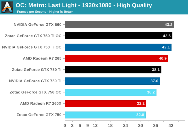
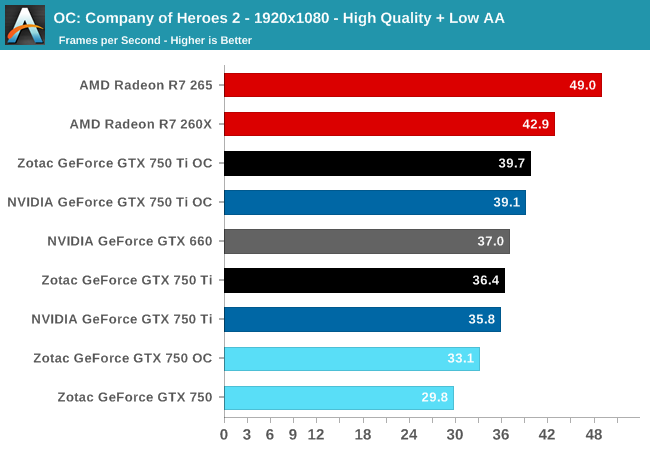
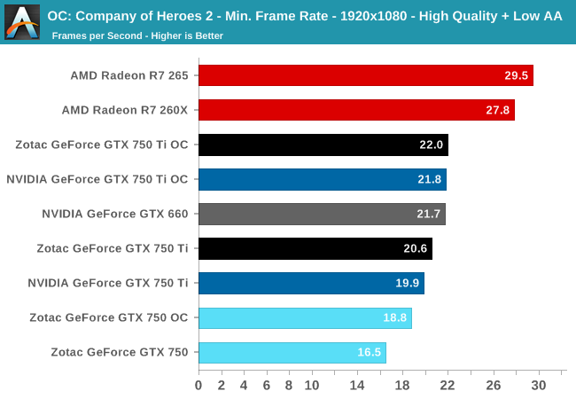
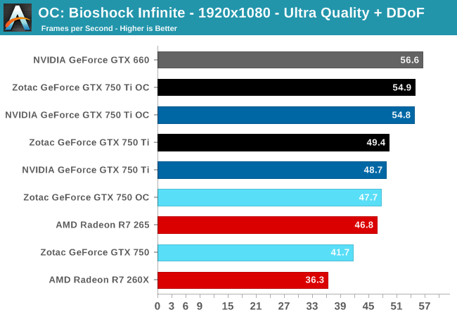
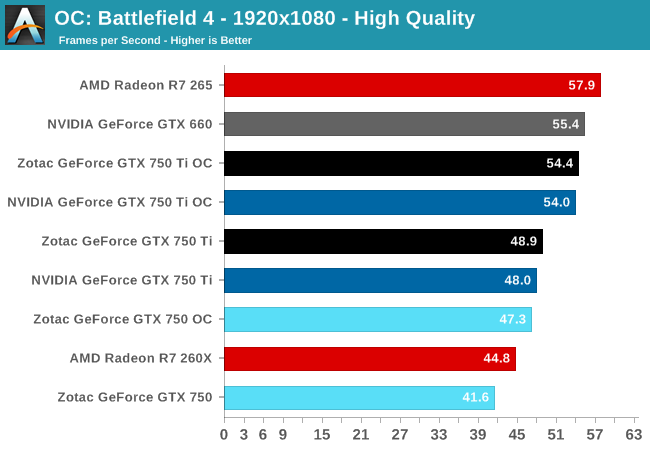
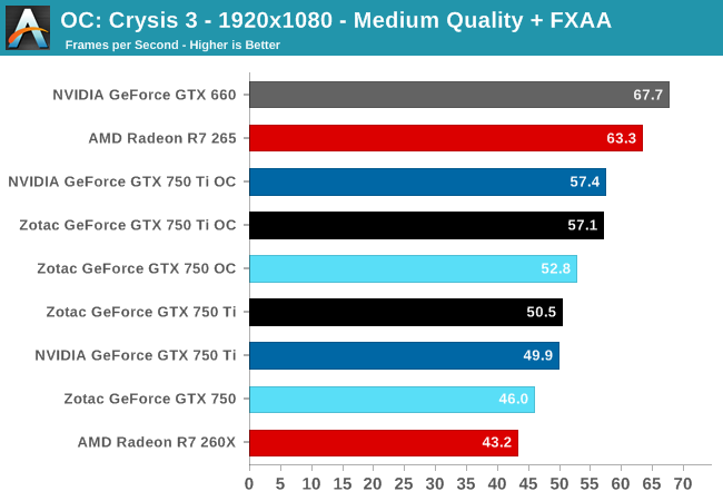
Depending on the game being used, the benefits from overclocking range from 9% to 12%, roughly in-line with our overclocks. For the GTX 750 this is sometimes enough to catch the stock clocked R7 260X, but even with this overclock the GTX 750 Ti will still generally trail the R7 265.
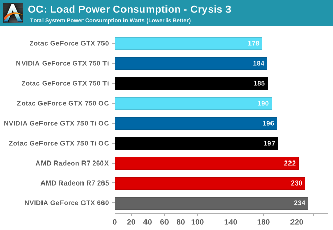
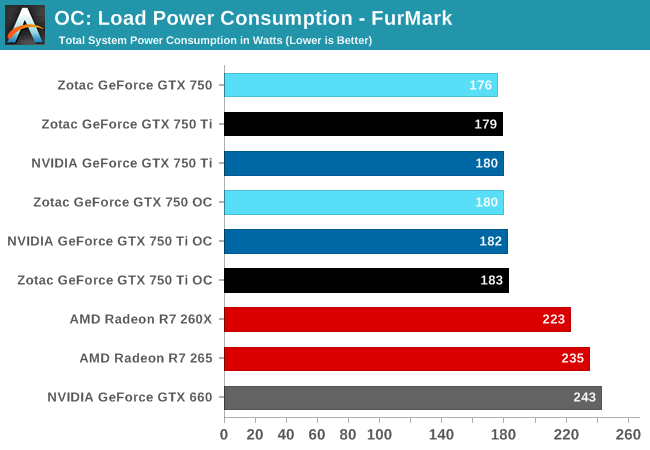
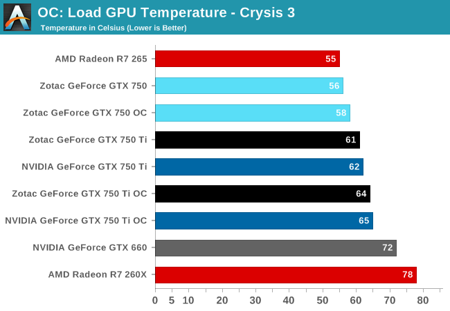
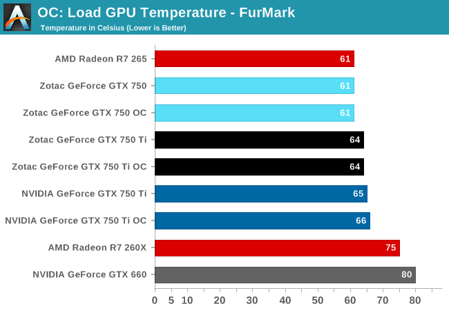
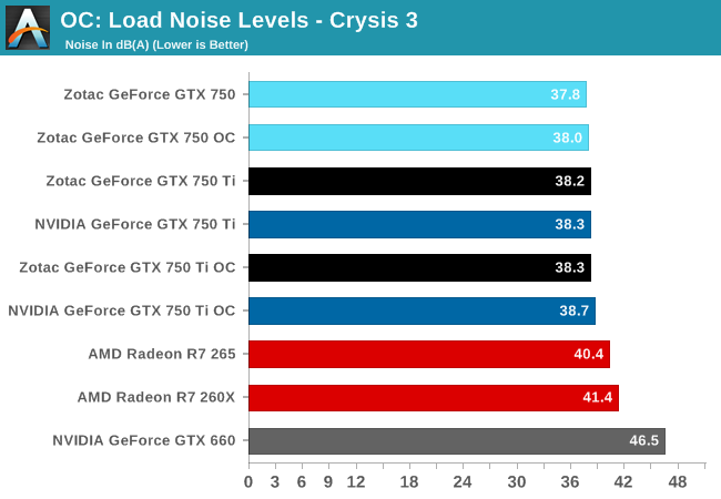
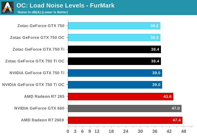
On the other hand, because of the hard TDP limit of 100%, this extra performance is relatively cheap. Video card power consumption moves by only a few watts, and then a few watts of CPU time on top of that. For all practical purposes overclocking can extend NVIDIA’s already incredible performance-per-watt ratio by another 10% with no meaningful impact on noise. Given the consistency of overclocking headroom we’ve seen in our GTX 750 series samples, this is one of those scenarios where overclocking is going to be a reasonable and (relatively) fool proof action to take.
Final Words
Bringing this review to a close, NVIDIA’s latest product launch has given us quite a bit to digest. Not only are we looking at NVIDIA’s latest products for the high volume mainstream desktop video card market, but we’re doing so through the glasses of a new generation of GPUs. With the GeForce GTX 750 series we are seeing our first look at what the next generation of GPUs will hold for NVIDIA, and if these cards are an accurate indication of what’s to follow then we’re being setup for quite an interesting time.
Starting from an architectural point of view, it’s clear from the very start that Maxwell is both a refresh of the Kepler architecture and at the same time oh so much more. I think from a feature perspective it’s going to be difficult not to be a bit disappointed that NVIDIA hasn’t pushed the envelope here in some manner, leaving us with a part that as far as features go is distinctly Kepler. Complete support for Direct3D 11.1 and 11.2, though not essential, would have been nice to have so that 11.2 could be the standard for new video cards in 2014. Otherwise I’ll fully admit I don’t know what else to expect of Maxwell – the lack of a new Direct3D standard leaves this as something of a wildcard – but it means that there isn’t a real marquee feature for the architecture to evaluate and marvel at.
On the other hand, the lack of a significant feature changes means that it’s much easier to evaluate Maxwell next to Kepler in the area where NVIDIA did focus: efficiency. This goes for power efficiency resource/compute efficiency, and space efficiency. Utilizing a number of techniques NVIDIA set out to double their performance per watt versus Kepler – a design that was already power efficient by desktop GPU standards – and it’s safe to say that they have accomplished this. With a higher resource efficiency giving NVIDIA additional performance with less hardware, and power optimizations bringing that power consumption down by dozens of watts, NVIDIA has done what in previous generations would have taken a die shrink. The tradeoff is that NVIDIA doesn’t have that die shrink, so die sizes grow in the process, but even then the fact that they packed so much more hardware into GM107 for only a moderate increase in die size is definitely remarkable from an engineering perspective.
Efficiency aside, Maxwell’s architecture is something of an oddity at first, but given NVIDIA’s efficiency gains it’s difficult to argue with the outcome. The partitioning of the SMM means that we have partitions that feel a lot like GF100 SMs, which has NVIDIA going backwards in a sense due to the fact that significant resource sharing was something that first became big with Kepler. But perhaps that was the right move all along, as evidenced by what NVIDIA has achieved. On the other hand the upgrade of the compute feature set to GK110 levels is good news all around. The increased efficiency it affords improves performance alongside the other IPC improvements NVIDIA has worked in, plus it means that some of GK110’s more exotic features such as dynamic parallelism and HyperQ are now a baseline feature. Furthermore the reduction in register pressure and memory pressure all around should be a welcome development; compared to GK107 there are now more registers per thread, more registers per CUDA core, more shared memory per CUDA core, and a lot more L2 cache per GPU. All of which should help to alleviate memory related stalls, especially as NVIDIA is staying on the 128-bit bus.
With that in mind, this brings us to the cards themselves. By doubling their performance-per-watt NVIDIA has significantly shifted their performance both with respect to their own product lineup and AMD’s lineup. The fact that the GTX 750 Ti is nearly 2x as fast as the GTX 650 is a significant victory for NVIDIA, and the fact that it’s nearly 3x faster than the GT 640 – officially NVIDIA’s fastest 600 series card without a PCIe power plug requirement – completely changes the sub-75W market. NVIDIA wants to leverage GM107 and the GTX 750 series to capture this market for HTPC use and OEM system upgrades alike, and they’re in a very good position to do so. Plus it goes without saying that compared to last-generation cards such as the GeForce GTX 550 Ti, NVIDIA has finally doubled their performance (and halved their power consumption!), for existing NVIDIA customers looking for a significant upgrade from older GF106/GF116 cards.
But on a competitive basis things are not so solidly in NVIDIA’s favor. NVIDIA does not always attempt to compete with AMD on a price/performance basis in the mainstream market, as their brand and retail presence gives them something they can bank on even when they don’t have the performance advantage. In this case NVIDIA has purposely chosen to forgo chasing AMD for the price/performance lead, and as such for the price the GeForce GTX 750 cards are the weaker products. Radeon R7 265 holds a particularly large 19% lead over GTX 750 Ti, and in fact wins at every single benchmark. Similarly, Radeon R7 260X averages a 10% lead over GTX 750, and it does so while having 2GB of VRAM to GTX 750’s 1GB.
On a pure price/performance basis, the GTX 750 series is not competitive. If you’re in the sub-$150 market and looking solely at performance, the Radeon R7 260 series will be the way to go. But this requires forgoing NVIDIA’s ecosystem and their power efficiency advantage; if either of those matter to you, then the lower performance of the NVIDIA cards will be justified by their other advantages. With that said however, we will throw in an escape clause: NVIDIA has hard availability today, while AMD’s Radeon R7 265 cards are still not due for about another 2 weeks. Furthermore it’s not at all clear if retailers will hold to their $149 MSRP due to insane demand from cryptocoin miners; if that happens then NVIDIA’s competition is diminished or removed entirely, and NVIDIA wins on price/performance by default.
Wrapping things up, as excited as we get and as focused as we are on desktop cards, it’s hard not to view this launch as a preview of things to come. With laptop sales already exceeding desktop sales, it’s a foregone conclusion that NVIDIA will move more GM107 based video cards in mobile products than they will in desktops. With GK107 already being very successful in that space and GM107 doubling NVIDIA’s performance-per-watt – and thereby doubling their performance in those power-constrained devices – it means that GM107 is going to be an even greater asset in the mobile arena. To that end it will be very interesting to see what happens once NVIDIA starts releasing the obligatory mobile variants of the GTX 750 series, as what we’ve seen today tells us that we could be in for a very welcome jump in mobile performance.

