Original Link: https://www.anandtech.com/show/7742/im-intelligent-memory-to-release-16gb-unregistered-ddr3-modules
I'M Intelligent Memory to release 16GB Unregistered DDR3 Modules
by Ian Cutress on February 11, 2014 6:59 PM EST- Posted in
- Memory
- Modules
- 16GB
- 8Gb
- I'M Intelligent Memory

After talking about Avoton and Bay Trail on Twitter, I was approached by the company heading up the marketing and PR for I’M Intelligent Memory regarding a few new products in the pipeline different to what we had seen in the market previously. The big one in my book is that they are currently sampling 16GB unregistered DDR3 modules ready for ramping up production.
Currently in the consumer space we have 8GB unregistered modules, usually paired together for a 16GB kit. These use sixteen 4 Gb memory packages on board to total up to the 8 GB number, and are packaged in speeds up to 2933+ MT/s. Intelligent Memory are a company (or series of smaller individual companies) that have new IP in the market to tie two of these 4 Gb dies together into a 8 Gb die, and are thus able to double the capacity of memory available in the market.
I have been speaking with Thorsten Wronski, President of Sales and Technology at Memphis AG, the company heading up the business end of the Intelligent Memory plan. We went into detail regarding how the new IP works (as much as I could be told without breaking NDA):
DRAM stacking is unlike NAND stacking. We have seen manufacturers stick 16 NAND dies onto a single package, but DRAM requires precise (picosecond level) timing to allow the two 4 Gb dies to act as a single 8 Gb package. This is the new IP to the table, which can apply to both unregistered and registered memory, as well as ECC memory.
The JEDEC specifications for DDR3 do account for the use of 8 Gbit packages (either one 8 Gbit die or two 4 Gbit dies per package), should these be available. However I am told that currently there is a fundamental non-fixable issue on all Intel processors (except Avoton and Rangeley, other Silvermont (BayTrail) is affected) that means that these dies are not recognised. In their specifications for Ivy Bridge-E, Intel do state that 8Gb packages are supported (link, page 10), however this apparently has not been the case so far and I'M is working with motherboard manufacturers to further pin down this issue.
Typically the access of a memory chip requires a column and a row, both of which are multiplexed across a set of 16 connects. With a 4 Gbit package, to access the row, all 16 are used (A0 to A15), whereas a column uses 10 (A0 to A9). In the 8 Gbit package, the column also requires A11, all part of the JEDEC spec. This works on Avoton/Rangeley, but not on any other Intel processor, according to Intelligent Memory, and the exact nature of the issue is down to Intel’s implementation of the specification. I suspect that Intel did not predict 8 Gbit packages coming to market at this time, and have found an efficiency improvement somewhere along the line. Perhaps needless to say, Intel should be supporting the larger dies going forward.
The dies that I’M are using are 30nm, and according to them the reason why Hynix/Samsung et al have not released an 8 Gbit DRAM die up until this point is that they are waiting until 25nm in order to do so – this is why I’M is very excited about their product. It could also mean that users wanting HSA implementations under Kaveri could have access to 64GB of DRAM to play with. But it also means that when 8 Gbit 25nm DRAM dies become available, I’M will perhaps try for a 16 Gbit package for 32GB modules - all aimed for DDR4 I would imagine.
I’M Intelligent Memory is currently a couple of weeks out from sampling our server guru Johan with some of these modules, so hopefully we will get an insight from him as to how they are looking. They are intending to go down two routes with their product – selling the combined die packages and selling modules. I have been told that one of the normal end-user manufacturers has already expressed interest in the packages (rated at DDR3-1600), which they would place onto their own DRAM sticks and perhaps bin the ICs for higher speed. The modules will be sold also via a third-party that often deals in bulk sales.
Mass production is set to begin in March and April, with initial pricing per 16GB module in the $320-$350 range for both DIMM and SO-DIMM, ECC being on the higher end of that range. To put that into perspective, most DRAM modules on sale today for end-users are in the $8-$14/GB range, making the modules have a small premium which is understandable to get the higher density.
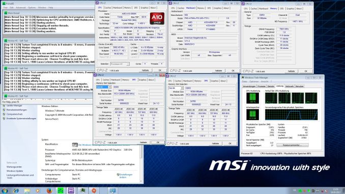
If this IP holds up to the standard, I would not be surprised if it is purchased (or at the very least observed) by the big DRAM manufacturers. I expect these modules will first see the light of day in servers (Avoton based most likely), and I will keep an eye out if any end-user manufacturers get a hold of some. I’M have verified the modules on AMD FX processors (FX-6300 and FX-8320 on 990FX/AM3+) as well as AMD's 760G and A75 (FM2 socket) chipsets. I was forwarded the following screenshot of two of these modules in an MSI FM2-A75MA-P33 motherboard, which is a dual DRAM module motherboard using the FM2 socket for Trinity APUs:
Here each of the 16GB modules (shown in the SPD tab of CPU-Z) are running at DDR3-1600 11-11-11, giving the two DRAM slot motherboard a total of 32GB of addressable space.
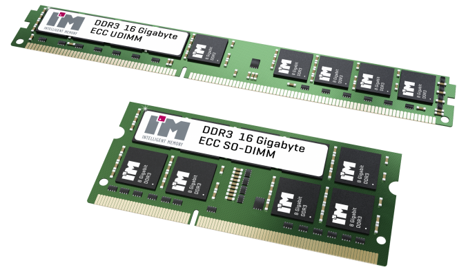
Aside from unregistered modules, I’M are also planning ECC UDIMM and RDIMM versions as well, such as 16GB very-low-profile RDIMMs and 16GB ECC SO-DIMMs. Non ECC SO-DIMMs are also being planned. A lot of their focus will be the supply of DRAM components for the direct integration onto automated systems where memory counts are fixed, for systems that use Marvell, TI, Freescale, Xilinx, Altera, Renesas and so on.


