Original Link: https://www.anandtech.com/show/7622/nvidia-tegra-k1
NVIDIA Tegra K1 Preview & Architecture Analysis
by Brian Klug & Anand Lal Shimpi on January 6, 2014 6:31 AM EST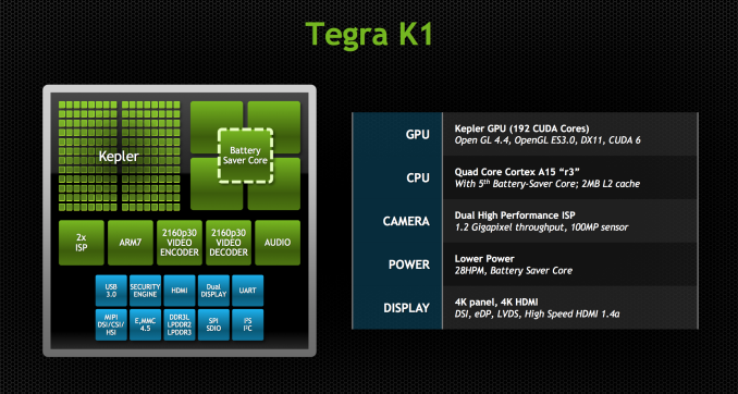
NVIDIA has taken to using CES as its platform for launching members of its Tegra mobile SoC family. This year was no different as it shifted branding a bit in its announcement of the Tegra K1, formerly known as Project Logan.
With Tegra 2 NVIDIA’s big selling point was being first to dual-core in Android. Tegra 3 attempted to do the same with being first to quad-core. Tegra 4 just made things faster. Tegra K1 on the other hand does away with the gimmicks and instead focuses on fundamentals.
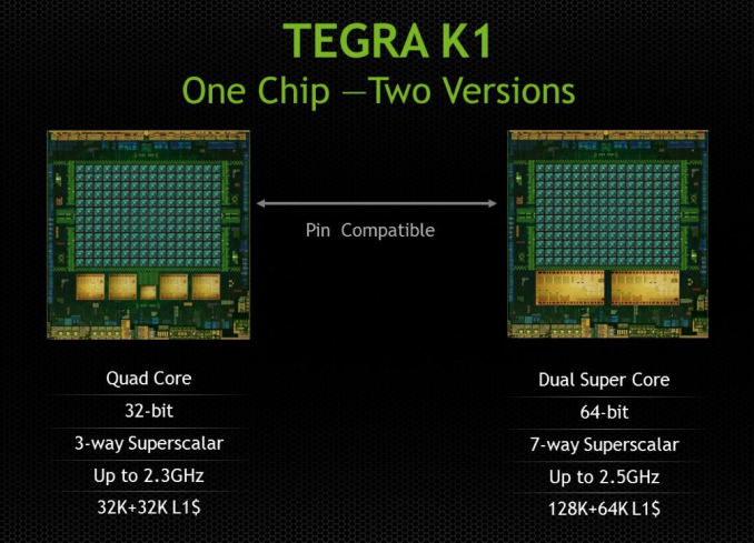
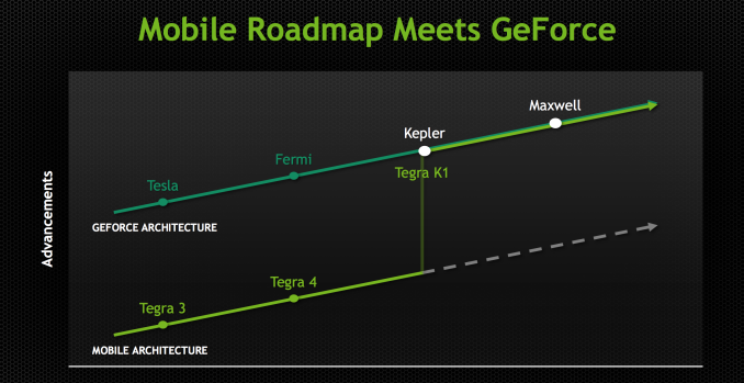
The SoC will come in two versions, one version with a quad-core (4+1) Cortex-A15, and one that leverages two of NVIDIA’s own 64-bit ARMv8 Denver CPUs. More importantly, they both ship with a full implementation of NVIDIA’s Kepler GPU architecture. In fact, Tegra K1 marks a substantial change in the way NVIDIA approaches mobile GPU design. From this point forward, all mobile GPUs will leverage the same architectures as NVIDIA’s desktop parts. As if that wasn’t enough, starting now, all future NVIDIA GeForce designs will begin first and foremost as mobile designs. NVIDIA just went from playing with mobile to dead serious in a heartbeat.
Tegra K1 will also be NVIDIA's launch vehicle for Project Denver, it's first fully custom ARMv8 CPU core. More on that in a bit.
CPU Option 1: Quad-Core ARM Cortex A15
Tegra K1 will ship in two configurations. The first went into production at the end of December 2013, is shipping to OEMs this quarter and will be in devices, allegedly, in the first half of 2014. This first configuration is based on ARM’s Cortex A15 CPU core.
Much like Tegra 4, the A15 version of Tegra K1 features four Cortex A15s synthesized for high frequencies and a fifth Cortex A15 that’s optimized for low power/frequency operation. The fifth core, what NVIDIA likes to call a shadow or companion core, is swapped in during periods of very low CPU usage (e.g. idle, screen off in your pocket updating new tweets/emails). As CPU demands grow the companion core is switched out for one of the four high performance cores, then two, then three and finally all four can be plugged in at once (but never five).
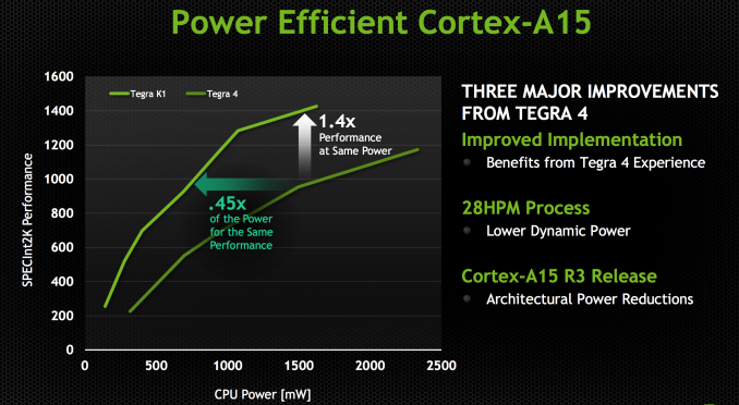
Tegra K1 ships with a newer revision of the Cortex A15 (r3p3) than what was in Tegra 4 (r2p1). ARM continuously updates its processor IP, with each revision bringing bug fixes and sometimes performance improvements. In the case of Tegra K1’s A15s, the main improvements here have to do with increasing power efficiency. With r3p0 (which r3p3 inherits) ARM added more fine grained clock gating, which should directly impact power efficiency.
The combination of the newer Cortex A15 revision and the move to 28nm HPM give Tegra K1 better performance at the same power consumption or lower power consumption at the same performance level. The reality tends to be that mobile OEMs will pursue max performance and not optimize for a good performance/power balance, but it’s at least possible to do better with Tegra K1 than with Tegra 4.
The max CPU clock goes up from 1.9GHz to 2.3GHz, a direct result of the move to 28nm HPM; 2.3GHz is the max CPU clock regardless of the number of active cores. The max performance increase over Tegra 4 running at max clocks will be just over 20%.
NVIDIA hasn’t made any changes to the L1/L2 cache configuration with Tegra K1. We’re still dealing with a shared 2MB L2 and 32KB/32KB L1s (I$+D$) per core.
The companion core can scale up to 1GHz, but tends to run at around 500MHz.
Feeding the CPU (and GPU) cores is a 64-bit wide LPDDR3 memory interface. NVIDIA will offer Tegra K1 in PoP, discrete and another package revision for standard clamshell notebook use.
CPU Option 2: Dual-Core 64-bit NVIDIA Denver
Three years ago, also at CES, NVIDIA announced that it was working on its own custom ARM based microprocessor, codenamed Denver. Denver was teased back in 2011 as a solution for everything from PCs to servers, with no direct mention of going into phones or tablets. In the second half of 2014, NVIDIA expects to offer a second version of Tegra K1 based on two Denver cores instead of 4+1 ARM Cortex A15s. Details are light but here’s what I’m expecting/have been able to piece together.
Given the 28nm HPM process for Tegra K1, I’d expect that the Denver version is also a 28nm HPM design. NVIDIA claims the two SoCs are pin-compatible, which tells me that both feature the same 64-bit wide LPDDR3 memory interface.
The companion core is gone in the Denver version of K1, as is the quad-core silliness. Instead you get two, presumably larger cores with much higher IPC; in other words, the right way to design a CPU for mobile. Ironically it’s NVIDIA, the company that drove the rest of the ARM market into the core race, that is the first (excluding Apple/Intel) to come to the realization that four cores may not be the best use of die area in pursuit of good performance per watt in a phone/tablet design.
It’s long been rumored that Denver was a reincarnation of NVIDIA’s original design for an x86 CPU. The rumor there being NVIDIA used binary translation to convert x86 assembly to some internal format (optimizing the assembly in the process for proper scheduling/dispatch/execution) before it hit the CPU core itself. The obvious change being instead of being x86 compatible, NVIDIA built something that was compatible with ARMv8.
I believe Denver still works the same way though. My guess is there’s some form of a software abstraction layer that intercepts ARMv8 machine code, translates and optimizes/morphs it into a friendlier format and then dispatches it to the underlying hardware. We’ve seen code morphing + binary translation done in the past, including famously in Transmeta’s offerings in the early 2000s, but it’s never been done all that well at the consumer client level.
Mobile SoC vendors are caught in a tough position. Each generation they are presented with opportunities to increase performance, however at some point you need to move to a larger out of order design in order to efficiently scale performance. Once you make that jump, there’s a corresponding increase in power consumption that you simply can’t get over. Furthermore, subsequent performance increases usually depend on leveraging more speculative execution, which also comes with substantial power costs.
ARM’s solution to this problem is to have your cake and eat it too. Ship a design with some big, speculative, out of order cores but also include some in-order cores when you don’t absolutely need the added performance. Include some logic to switch between the cores and you’re golden.
If Denver indeed follows this path of binary translation + code optimization/morphing, it offers another option for saving power while increasing performance in mobile. You can build a relatively wide machine (NVIDIA claims Denver is a 7-issue design, though it’s important to note that we’re talking about the CPU’s internal instruction format and it’s not clear what type of instructions can be co-issued) but move a lot of the scheduling/ILP complexities into software. With a good code morphing engine the CPU could regularly receive nice bundles of instructions that are already optimized for peak parallelism. Removing the scheduling/OoO complexities from the CPU could save power.
Granted all of this funky code translation and optimization is done in software, which ultimately has to run on the same underlying CPU hardware, so some power is expended doing that. The point being that if you do it efficiently, any power/time you spend here will still cost less than if you had built a conventional OoO machine.
I have to say that if this does end up being the case, I’ve got to give Charlie credit. He called it all back in late 2011, a few months after NVIDIA announced Denver.
NVIDIA announced that Denver would have a 128KB L1 instruction cache and a 64KB L1 data cache. It’s fairly unusual to see imbalanced L1 I/D caches like that in a client machine, which I can only assume has something to do with Denver’s more unique architecture. Curiously enough, Transmeta’s Efficeon processor (2nd generation code morphing CPU) had the exact same L1 cache sizes (it also worked on 8-wide VLIW instructions for what it’s worth). NVIDIA also gave us a clock target of 2.5GHz. For an insanely wide machine 2.5GHz sounds pretty high, especially if we’re talking about 28nm HPM, so I’m betting Charlie is right in that we need to put machine width in perspective.
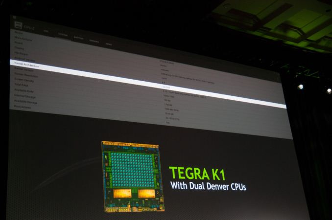
NVIDIA showed a Denver Tegra K1 running Android 4.4 at CES. The design came back from the fab sometime in the past couple of weeks and is already up and running Android. NVIDIA hopes to ship the Denver version of Tegra K1 in the second half of the year.
The Denver option is the more interesting of the two as it not only gives us another (very unique) solution to the power problem in mobile, but it also embraces a much more sane idea of the right balance of core size vs. core count in mobile.
The GPU
Despite the Denver surprise, the big story behind Tegra K1 is its GPU. Prior to K1, all previous Tegra designs implemented some derivative of what became known as the GeForce ULP core. This was a non-unified architecture that, at times, looked a lot like NV40. The design was never all that impressive from a performance or power efficiency standpoint. It was cost effective and often constrained by a narrow memory interface.
Going into Project Logan, which became Tegra K1, NVIDIA made the decision (around 3 years ago) to abandon the GeForce ULP roadmap and instead combine mobile and PC GPU roadmaps. Tegra K1 would be the first design to leverage a PC GPU, in this case Kepler. The bigger implication is that all future Tegra SoCs will integrate PC GPUs. The even crazier part of all of this is that all future NVIDIA GPUs will start out as mobile first designs (including Maxwell). Productization and market availability may happen in a different order, but all architectures will start as mobile designs and then be adopted to fit other, higher power segments. This is very much like Intel’s mobile-first realization of the mid-2000s with regards to notebook processors, but with NVIDIA and smartphone/tablet GPUs.
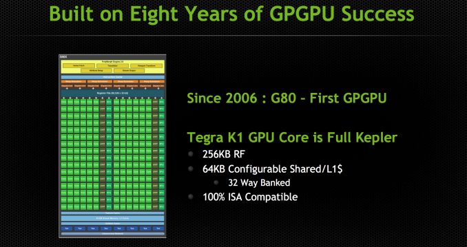
Kepler makes the move into mobile largely unchanged. This is a full Kepler implementation with the same size register file, shared L1 and is 100% ISA compatible with its big brother. It turns out that Kepler, as it was originally designed, was pretty good for mobile. If you take a GeForce 740M (2 SMX/384 CUDA core design), you’re looking at roughly a 19W GPU. Of that 19W, around 3W is memory IO, PCIe and other non-GPU things. You can subtract another 6W for leakage, bringing you down to 10W. Now that’s a 2 SMX design, so divide it in half and now you’re down to 5W. Drop the clock from 1GHz down to 900MHz, and the voltage as well, and now we’re talking around 2 - 3W for the GPU core and that’s without any re-architecting. Granted you can’t just subtract out things like leakage like that, but you get the point. Kepler wasn’t a bad starting point for a good mobile GPU design.
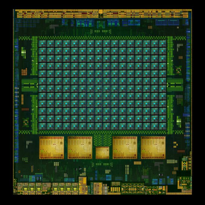
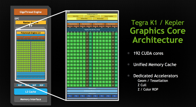
Tegra K1 features a single SMX (in a single GPC), which amounts to 192 CUDA cores. NVIDIA made the rookie mistake of calling Tegra K1 a 192-core processor, which made for some great headlines but largely does the industry a disservice.
Tessellation and geometry engines aren’t crippled compared to desktop Kepler. FP64 support is also present, at 1/24 the FP32 rate. There are 4 ROPs and 8 texture units, down from 16 in the PC version of Kepler. The big changes however are in the interconnects between all of the parts of the GPU.
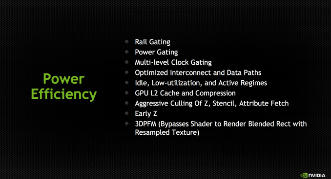
The bigger implementations of Kepler have to be able to efficiently move data between multiple SMXes, ROPs and memory controllers. The interconnect fabric needed to do that doesn’t scale down well for mobile, where in many cases we’re dealing with one or two of those things instead of a dozen. By removing the complexity that exists in the bigger Kepler’s fabric you limit the ability for mobile Kepler to scale, but then again mobile Kepler is never going to scale to the sizes of big desktop GPUs so it’s not an issue. There are other changes outside of interconnect, with improved clock gating among other focuses on power efficiency.
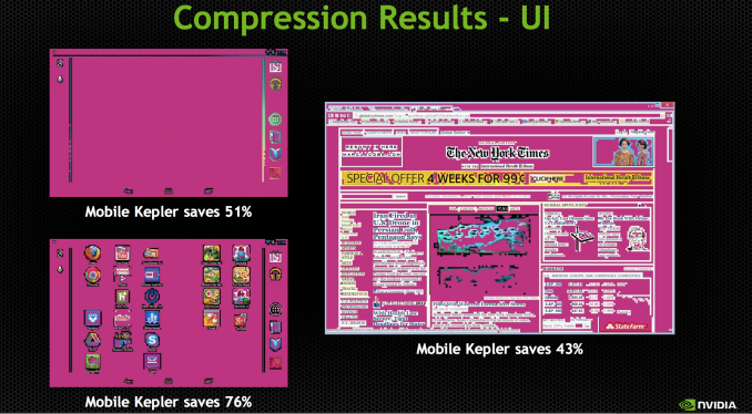
NVIDIA updated the texture units to support ASTC, something that isn’t present in the desktop Kepler variants at this point. NVIDIA also hopes to use the GPU’s color compression features to reduce memory bandwidth requirements in UI rendering and not just 3D games.
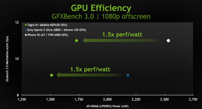
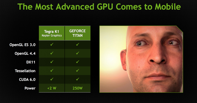
With the changes NVIDIA made to the design, Kepler ends up being a < 2W GPU perfect for mobile. NVIDIA provided us with some data showing SoC + DRAM power while running GFXBench 3.0 (Manhattan), an OpenGL ES 3.0 test:
The data is presented in NVIDIA’s usual way where we’re not looking at peak performance but rather how Tegra K1 behaves when normalized to the performance of Apple’s A7 or Qualcomm’s Snapdragon 800. In both cases NVIDIA is claiming the ability to deliver equal performance at substantially better power efficiency.
NVIDIA shared some live demos that echoed the data above. Peak performance was capped to that of the A7 or Snapdragon 800, but SoC level power was always lower. It remains to be seen what power consumption looks like in a shipping configuration (which is almost always optimized for peak performance not equal performance at lower power), but it’s safe to say that concerns about Kepler being too power hungry for mobile are overrated.
The most compelling argument in favor of putting Kepler in a mobile SoC actually has to do with its API support. In one swift move NVIDIA goes from being disappointing in API support to industry leading. Since this is a full Kepler implementation (just a lower power/performing version) Tegra K1 maintains full API compatibility with NVIDIA’s flagship GeForce products. OpenGL ES 3.0 is supported but so are full OpenGL 4.4, DX11 and CUDA 6.0.
NVIDIA made it a point to say that high-end games developed for the PC or even current generation consoles could be ported over to Tegra K1 without issue. It’s perhaps over reaching a bit to claim the latter given the delta in performance (which NVIDIA hopes to make up in 4 generations!), but you can definitely argue that titles built for the previous generation of consoles (Xbox 360/PS3) could easily be ported to Tegra K1.
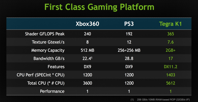
At its CES press conference NVIDIA teased the idea that Tegra K1 is actually more powerful than the last generation of consoles. The slide below attempts to drive that point home:
With a GPU clock of 950MHz (admittedly, a bit on the high end), NVIDIA can deliver substantially more raw horsepower than either previous generation console (192 CUDA cores * 2 FLOPS per core * 950MHz). Peak texture filtering performance and more importantly, memory bandwidth are lower than what was possible on these consoles but the numbers we’re talking about here aren’t substantial enough to prevent porting from happening. There may be some optimization needed but it definitely looks like Tegra K1 is the first mobile platform that can more or less run Xbox 360/PS3 titles, at least from a performance standpoint.
In pursuit of making porting and game development as simple as possible, NVIDIA demonstrated its NSight Tegra plugins for Visual Studio. Without changing the IDE that developers are used to, NSight Tegra allows developers to use the NDK toolchain all within Visual Studio. I’m not enough of a developer to know whether or not NVIDIA’s efforts in this space truly make life easy enough to port Xbox 360/PS3 games over to Android, but its VS integration demos looked convincing at least.
NVIDIA had a port of Serious Sam 3 running on Tegra K1 demo hardware just fine. Any games that are prepped for Steam OS are very easy to port over to Android. Once you make the move to OpenGL, the rest is allegedly fairly simple. The Serious Sam 3 port apparently took a matter of a couple of weeks to get ported over, with the bulk of the effort going into mapping controls to an Android environment.
Tegra K1 ISP & Video
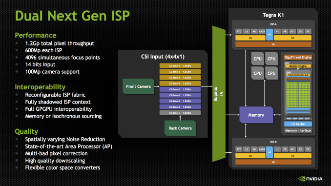
NVIDIA’s Tegra K1 SoC also makes some dramatic improvements on the ISP side. We saw SoCs start arriving with two ISPs sometime in 2013, which allowed OEMs to deliver a host of new imaging experiences, like shot in shot video and simultaneous use of both front and rear cameras. With Tegra K1, NVIDIA is not only moving to two ISPs, but it’s also making ISP more of a first class citizen.
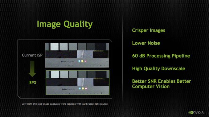
For those not familiar, ISP (Image Signal Processor) handles the imaging pipeline for still photos, video, and performs tasks like Bayer to RGB conversion (demosaicing), 3A (Autofocus, Auto Exposure, Auto white balance), noise reduction, lens correction, and so on. Although NVIDIA has always included an ISP onboard, I couldn’t shake the feeling that still imaging performance could’ve been better, especially in the few cases that allowed direct comparison (HTC One X). With Tegra K1, there’s more die area dedicated to ISP than in the past, and there are two of them to support the kind of dual camera applications that have quickly become popular.
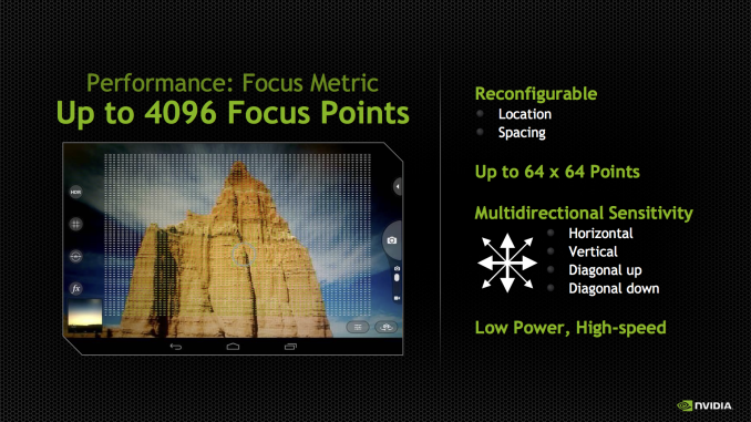
Tegra K1 includes the third generation of NVIDIA’s ISP, capable of processing 600 MP/s on each ISP with 14 bit input, and support for up to 100 MP cameras. There are two of them, so NVIDIA quotes the total pixel throughput as up to 1.2 Gp/s. This is dramatically increased from Tegra 4, which supported up to 400 Mp/s at 10 bits per pixel. In addition the K1’s ISP now supports up to 4096 focus points, a 64x64 array, for its autofocus routine. The ISP also has better noise reduction, and local tone mapping, a feature we’ve also seen become popular for combining parts of images and recovering some of the dynamic range lost with ever shrinking pixel sizes.
Tegra K1 retains compatibility with the Chimera 1.0 features that we just saw in the Tegra Note 7, like object tracking, always-on HDR, slow motion capture, and full resolution burst, and adds more. NVIDIA has kept the Chimera brand for the K1 SoC, calling it Chimera 2.0, and envisions this architecture enabling things like better temporal pixel binning (combining 8 exposures from the CMOS to drive noise down further), faster panorama, video stabilization, and even better live preview with effects applied. The high level of Chimera seems to be the same – kernels that either run on the CPU, or on the GPU (ostensibly in CUDA this time) before or after the ISP and in a variety of image spaces (Bayer or RGB depending).
On the video side, Tegra K1 continues to support 2160p30 (4K or UHD video at 30FPS) encode and decode. Broken down another way, H.264 High Profile Level 5.1 decode and 4K H.264 High Profile 4.2 encode. The fact that there’s a Kepler next door made me suspect that NVENC was used for most of these tasks, but it turns out that NVIDIA still has discrete blocks for video encode of H.264, VP8, VC1, and others. These are the same video encode and decode blocks as what were used in Tegra 4, but with some further optimizations for power and efficiency. The Tegra K1 platform includes support for H.265 video decode as well, but this isn’t accelerated fully in hardware, rather the decode is split across NVENC and CPU.
NVIDIA showed off a K1 reference board doing 4Kp30 H.264 decode on an attached display, I didn’t notice any dropped frames. Of course that’s a given considering we saw the same thing on Tegra 4, but it’s still worth noting that the SoC is capable of driving 4K/UHD displays over eDP 1.4, LVDS and HDMI 1.4b.
The full GPIO breakdown for Tegra K1 includes essentially all the requisite connectivity you’d expect for a mobile SoC. For USB there’s 3 USB 2.0 ports, and 2 USB 3.0 ports. For storage Tegra K1 supports eMMC up to version 4.5.1, and there’s PCIe x4 which can be configured
Final Words
NVIDIA’s challenge with Tegra has always been getting design wins. In the past NVIDIA offered quirky alternatives to Qualcomm, most of the time at a more attractive price point. With Tegra K1, NVIDIA offers a substantial feature and performance advantage thanks to its mobile Kepler GPU. I still don’t anticipate broad adoption in the phone space. If NVIDIA sees even some traction among Android tablets that’s enough to get to the next phase, which is trying to get some previous generation console titles ported over to the platform.
NVIDIA finally has the hardware necessary to give me what I’ve wanted ever since SoC vendors first started focusing on improving GPU performance: the ability to run Xbox 360 class titles in mobile. With Tegra K1 the problem goes from being a user interface, hardware and business problem to mostly a business problem. Android support for game controllers is reasonable enough, and K1 more or less fixes the hardware limitations, leaving only the question of how do game developers make enough money to justify the effort of porting. I suspect if we’re talking about moving over a library of existing titles that have already been substantially monetized, there doesn’t need to be all that much convincing. NVIDIA claims it’s already engaged with many game developers on this front, but I do believe it’ll still be an uphill battle.
If I were in Microsoft’s shoes, I’d view Tegra K1 as an opportunity to revolutionize my mobile strategy. Give users the ability to run games like Grand Theft Auto V on a mobile device in the not too distant future and you’ve now made your devices more interesting to a large group of users. I don’t anticipate many wanting to struggle to play console games on a 5-inch touchscreen, but with a good controller dock (or tablet with a kickstand + wireless controller) the interface problem goes away.
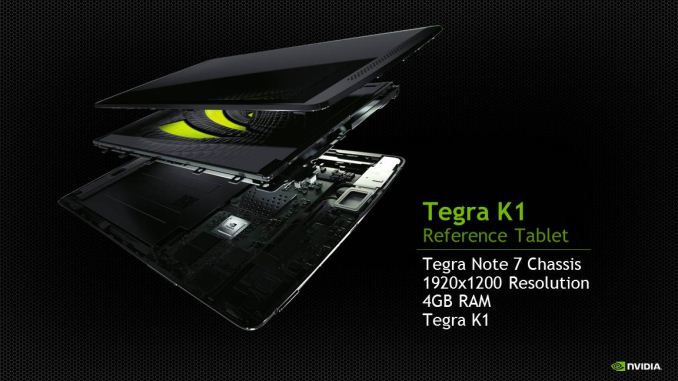
For the first time I’m really excited about an NVIDIA SoC. It took the company five generations to get here, but we finally have an example of NVIDIA doing what it’s really good at (making high performance GPUs) in mobile. NVIDIA will surely update its Tegra Note 7 to a Tegra K1 version (most of its demos were run in a Tegra Note 7 chassis), but even if that and Shield are the best we get the impact on the rest of the market will be huge. With Tegra K1, NVIDIA really raised the bar on the GPU performance.
The CPU side, at least for the Cortex A15 version is less interesting to me. ARM’s Cortex A15, particularly at high clocks, has proven to be a decent fit for tablets. I am curious to see how the Denver version of Tegra K1 turns out. If the rumors are true, Denver could very well be one of the biggest risks we’ve seen taken in pursuit of building a low power mobile CPU. I am eager to see how this one plays out.
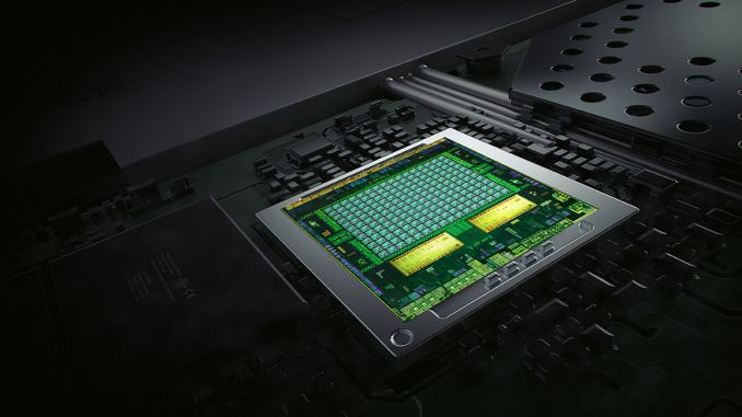
Finally: two big cores instead of a silly number of tiny cores
NVIDIA hasn’t had the best track record of meeting shipping goals on previous Tegra designs. I really hope we see Tegra K1, particularly the Denver version, ship on time (although I'm highly doubtful this will happen - new custom CPU core, GPU and process all at the same time?). I’m very eager not only for an install base of mobile devices with console-class GPUs to start building, but also to see what Denver can do. I suspect we’ll find out more at GTC about the latter. It’s things like Tegra K1 that really make covering the mobile space exciting.

