Original Link: https://www.anandtech.com/show/755
ASUS CUV266 Socket-370 Apollo Pro 266 ATX
by Mike Andrawes on April 18, 2001 12:50 AM EST- Posted in
- Motherboards
Introduction
DDR SDRAM is making a strong push as the memory of the future, especially in the Socket-A motherboard market thanks to chipsets from AMD, VIA, and ALi. Pro 266For those Intel CPU fans out there, a viable DDR solution has not been available until the recent introduction of the VIA Apollo Pro 266. As we found in our VIA Apollo Pro 266 Review, from a performance point of view, there’s really no reason for you to upgrade if you’ve already got a good i815 motherboard and PC133 SDRAM. The simple fact of the matter is that the Pentium III cannot take full advantage of memory bandwidth beyond PC133 due to its 133MHz FSB limitation. Nevertheless, the Apollo Pro 266 provides a healthy alternative to the i815 chipset, provided that the price of DDR SDRAM drops close to that of ordinary PC133 SDRAM in the near future. Of course, the Apollo Pro 266 does give you the option of buying DDR SDRAM now that you may be able to reuse in the future, whereas PC133 is looking more and more like a dead end all the time.
A couple weeks ago, we looked at the Gigabyte GA-6RX, an Apollo Pro 266 board that offers decent performance and features at a reasonable price. With several other Apollo Pro 266 boards lying in the AnandTech Labs, the ASUS CUV266 caught our eyes. Being just released during CEBIT 2001, ASUS seems to have put a lot of effort into making this board a nice alternative to their CUSL2, our Editor’s Choice for the best i815E motherboard. Without further ado, let’s take a close look at this motherboard and see if it can live up to those lofty standards.
|
ASUS
CUV266
|
|
|
CPU
Interface
|
Socket-370 |
|
Chipset |
VIA
Apollo Pro266 |
|
Form Factor |
ATX |
|
Bus Speed |
66 - 193MHz (in 1MHz increments) |
|
Core Voltages Supported |
Auto
Detect |
|
Memory Slots |
3 184-pin DDR DIMM Slots |
|
Expansion Slots |
1
AGP Slot |
|
On-board Audio |
C-Media CMI8738 |
|
BIOS |
Award Medallion BIOS 6.0 |
A unique layout
In an attempt to improve performance and stability, ASUS sometimes comes up with a unique PCB design. A good example is the ASUS A7V and A7V133, where they introduced a vertically mounted daughterboard containing the CPU’s power regulator. The CUV266 is yet another example of this - instead of the traditional location of the DIMM slots parallel to the front edge of the board, they are now placed parallel to the right edge of the motherboard.

While this placement was probably chosen because it allows for shorter trace lengths between the North Bridge, CPU, and memory, it also avoids one major problem we’ve seen on a number of motherboard, where the DIMM slots are placed too close to the AGP slot, making it impossible to add or remove memory after the video card is installed. With the design of the CUV266, inserting memory is never a problem regardless of the video card’s status.
ASUS put the power supply connector in front of the North Bridge, so the power cables will not have to run over the memory or CPU, and thus it not block airflow around the CPU. They’ve also left quite a bit of space around the CPU socket, so you should have no problem installing any kind of HSF unit. Note that the memory will still have to be removed to install most HSF units.
Unfortunately, we do have a major complaint about the hefty 12 by 9.5 inch PCB. As you can see in the picture, quite a bit of space on the right side of the board is wasted. The original revision of the board had two 168-pin DIMM slots (for standard SDR SDRAM) in this space. It's not clear exactly why they were removed, but they may make a come back in a different version of the board, although we have not been able to confirm this as of now. This "wasted" space merely contributes to the manufacturing cost of the motherboard and likely could have been used more efficiently, possibly by adding another PCI slot and shifting everything to the right a bit.
The two IDE connectors are located in front of the North Bridge, so they do not block any expansion slots. On the other hand, the floppy connector is placed vertically in front of the PCI slots, but since it is located between second and third PCI slots, it shouldn’t block the use of most full-length cards in those slots. Since all front panel connectors are placed vertically along the left edge of the board, you will be able to use full-length PCI devices in all five PCI slots.
The New Choice for Pentium III: Apollo Pro 266
The VIA 8633 North Bridge provides official support for 133MHz FSB Pentium III’s as well as DDR SDRAM and AGP 4X. One big advantage of the Apollo Pro 266 over the i815 is that its 8633 North Bridge supports a full 4GB of DDR SDRAM, rather than the i815’s paltry 512MB. Unfortunately, since 184-pin DDR SDRAM is still in the early stage compared to the traditional 168-pin SDRAM, large capacity modules are not readily available at the moment. With the common 128MB and 256MB modules that are available, packing 4GB of memory on Apollo Pro 266 motherboard is simply not possible. ASUS did include three DDR DIMM slots, so you should be able to install a total of 768MB memory. With 512MB modules on the way, 1.5GB should be easily reachable as well.
Just like all the other Apollo Pro 266 boards we’ve seen, the CUV266 allows you to run the CPU and the memory asynchronously. That’s good news because now you can take advantage of PC2100 DDR SDRAM using a 100MHz FSB Pentium III. However, as we've noticed in recent investigations, running your FSB and memory buses asynchronously can cause a significant memory latency penalty which could negate any performance gains you'd get from the higher bandwidth memory.
Speaking of memory, because of VIA's partnership with Nanya, ASUS is able to bundle a 128MB PC2100 DDR SDRAM stick using Nanya chips with the CUV266. ASUS has informed us that this is how all CUV266s will ship, however they may have a version without the bundled DDR SDRAM available in the future. It seems like this is an attempt by VIA to mimic Intel in their bundling of RDRAM with Pentium 4 processors.

The 8633 North Bridge also controls the AGP bus, and to ensure compatibility with all video cards on the market, ASUS went ahead and included an AGP Pro slot. Although there aren’t many video cards that require the added power supplied by AGP Pro. The AGP Pro slot is not keyed for 1.5V or 3.3V devices, so you should have no problem installing any AGP card.
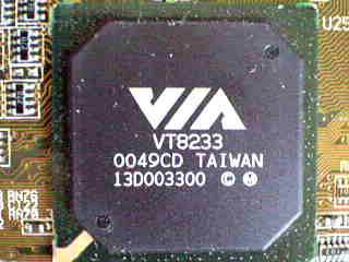
VIA’s 8233 South Bridge
The Apollo Pro 266 is also the first demonstration of VIA”s V-link, a dedicated channel between the 8633 North Bridge and the 8233 South Bridge rather than just using the PCI bus to connect the two. It’s very similar to Intel Hub Architecture (IHA) and moves the PCI bus interface to the South Bridge. Besides the PCI interface, the 8233 South Bridge also provides two Ultra ATA 100 channels supporting up to four IDE devices (two per channel) and three USB root hubs (6 USB ports total).
The two traditional USB ports are still located at the back, within the ATX I/O panel, while two extra USB headers are found on the left side of the board. You will need to use an USB bracket to enable the two USB ports available from each header, so you will need two brackets to take advantage of all four USB ports. In the past, ASUS has included at least one USB header, although none with this early evaluation sample.
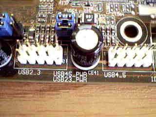
Headers for the second and third USB root hub.
The 5/1/0/1 (PCI/AGP/ISA/ACR) expansion slot configuration has been spotted on several Apollo Pro 266 motherboards, which should be enough for most system configurations, although six PCI slots with or without the ACR slot would be even better in the minds of most AnandTech readers.
ASUS has always been one of the biggest OEM suppliers in the market, and that’s exactly why they continue to include an ACR slot. ACR is VIA’s answer to the Intel’s CNR slot, and its advantage is that the slot itself is actually an inverted PCI slot, so manufacturers do not have to produce a special slot design and thus reducing the cost. Older AMR cards can work in an ACR slot as well.
In terms of on-board audio, ASUS went a step beyond the common AC’97 host-based CODECs we usually see and made the C-Media CMI8738 hardware-based sound chip optional. For better audio , especially in games, we still recommend something like a Creative Labs Sound Blaster Live!

C-Media on-board audio.
ASUS: The King of Overclocking
Besides being one of the largest OEM manufacturers, ASUS is also one of the favorites for hardware enthusiasts thanks to their products’ great stability and overclocking options. While they have been “one upped” at times by other manufacturers, such as ABIT, they have been doing their best to pick up the slack recently, and the CUV266 definitely puts ASUS right back at the top.
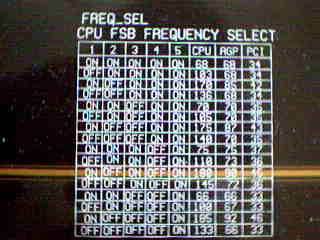
Following what has almost become “tradition,” ASUS allows both jumperless overclocking and overclocking by dipswitches. If you set the jumpers on the motherboard to jumperless mode, you will be able to adjust the FSB from inside the BIOS. Since most Intel chips are multiplier locked (engineering samples are the exception), it is very important to have a wide range of FSB speeds to maximize overclocking potential. ASUS did just that by providing 1MHz increments for the FSB between 66 and 193MHz. The PCI and AGP ratios are adjusted automatically so that these bus speeds are as close as possible to their default values of 33 and 66MHz, respectively.
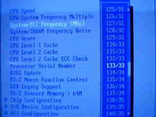
FSB speeds available in the BIOS in 1MHz increments.
In front of the fourth and fifth PCI slots, there is a set of dipswitches for changing the FSB speed. The available speeds are silk screened on the PCB as well, so you should be able to adjust the settings without consulting the manual. Unfortunately, not all the FSB speeds are available via the dipswitches, so BIOS overclocking is the better and easier way to go in most cases.
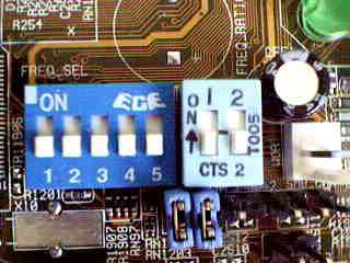
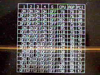
Dipswitches controlling the FSB speeds.
ASUS also put in a reasonable range of CPU core voltages, between 1.65 and 1.95V in 0.05V increments, to make the system more stable under overclocking situations. This is done within the BIOS and you can monitor the actual voltage that is being output in the BIOS as well. Besides the CPU core voltage, you can also read three temperatures and three fan speeds in the BIOS. The interesting part of the ASUS’s hardware monitoring setup is that they decided not to use the integrated hardware monitoring capabilities of the VIA 8233 South Bridge, but instead went with a custom ASIC, the AS99127F. The board offers three fan headers, one for the CPU’s HSF unit and two for chassis fans.
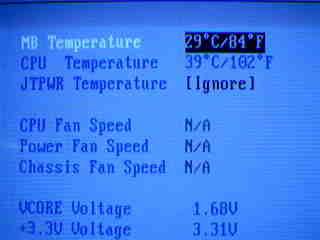
Hardware monitor in the BIOS.
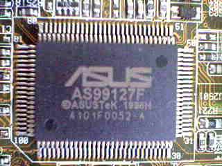
ASUS ASIC for hardware monitoring.
I/O voltage tweaking can also be very important in maintaining the stability of an overclocked system. This setting is available on the CUV266 through a set of jumpers on the board. The voltages available are 2.65V, 2.75V, and 2.9V, where 2.65V is the default setting. Notice that these voltages are much lower than the I/O voltages found on most other boards. This is due to the fact that DDR SDRAM runs at a lower 2.5V, while traditional SDRAM runs at 3.3V.
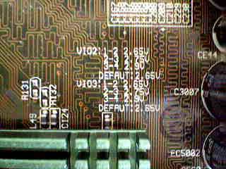
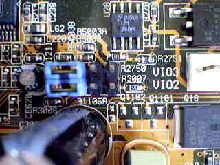
I/O voltage settings.
The CUV266 also offers a variety of options for memory tweaking. However, keep in mind that since DDR SDRAM is still in its infancy compared to traditional SDR SDRAM, current DDR memory may or may not be as tweakable as we’ve come to expect from SDR SDRAM. In our tests, pushing the memory settings wasn’t the best idea and readily degraded the stability of the test system.
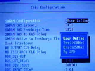
Memory tweaking options in the BIOS.
Overclocking on the CUV266 turned out to be quite good. With the CPU core and I/O voltages set to default and memory timings set to CAS2.5 with no memory interleaving, we were able to push the FSB of the system to 139MHz without any penalties on the stability of the system. With today’s Socket-A motherboards routinely pushing 150+ MHz FSB speeds, this seems extremely low. It currently appears that we’re limited by the DDR memory interface - whether the modules we’re using or something in the chipset is imposing that limitation remains to be seen. We’ll continue testing, and as soon as we know where the limitation is, we’ll let you know.
Pluses and Minuses
As the market gets more and more competitive, many manufacturers are trying to distinguish their boards from the rest of the crowd by including a variety of unique features. As such, an on-board IDE RAID controller is practically standard on a high-end board targeted at enthusiasts, while special diagnostic tools are also quite popular.
ASUS noticed these trends and decided to take a slightly different route by integrating an Ethernet controller. This is not entirely unheard of, and at one point, it actually looked like this would become a standard feature as networks have become much more common. ASUS always focuses on quality, so it’s no surprise that they went with a highly regarded name for the on-board Ethernet controller. In this case, it’s 3Com’s 3C-920 10/100Mbps controller. The controller chip is located behind the fourth PCI slot, and the Ethernet port is placed above the two USB ports within the ATX I/O panel. Unfortunately, ASUS did not include a special I/O shield with our sample, but we fully expect the shipping version to include one, but have not been able to confirm this fact with ASUS.
What is strange, however, is that VIA already has integrated 10/100 Ethernet in the 8233 South Bridge that is used on the CUV266. Why ASUS has chosen to go with an external control anyway is beyond us, but something that we’ve seen them do numerous times in the past with i815E boards, which also feature Ethernet in the ICH2.
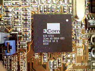
3Com 10/100Mbps Ethernet controller chip
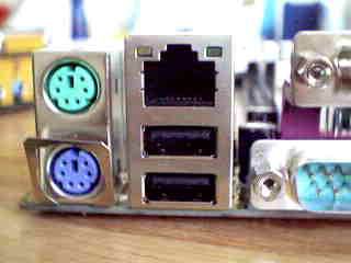
Ethernet port in the ATX I/O panel
Besides the excellent performance we have come to expect from ASUS products, their outstanding quality and stability are actually what makes their boards so popular. The CUV266 was no exception, as stability was very impressive during our testing. With a CAS latency of two and no memory interleaving, the system was rock solid and didn’t crash once in 24 hours. Recall that our Gigabyte GA-6RX was not stable at all at CAS2 with memory interleaving enabled, but that’s not the case here. With either two-bank and four-bank interleaving enabled, the CUV266 was still pretty solid, albeit not quite as good as without memory interleaving - we experienced two crashes during 24 hours of stress testing, still quite impressive compared to most other motherboards.
Unfortunately, we did run into a few problems with the CUV266, the biggest of which was with AGP 4X. With it enabled, the system would crash every time we installed the video driver. By dropping back to AGP 2X and using the latest VIA 4.29v 4-in-1 driver, the problem was solved. Luckily, AGP 4X does not offer much benefit over AGP 2X, and we did not notice a significant performance hit. Nevertheless, there’s clearly something wrong here and such a problem should not exist. Hopefully this can be corrected with a BIOS update.
Furthermore, we were actually a little bit disappointed that ASUS did not include on-board IDE RAID controller, which would have made this board a truly exceptional one.
ASUS has always had one of the best manuals among motherboard manufacturers. Although there was no manual included with our early sample, we fully expect to see the excellent ASUS manual that we’re used to, containing almost every piece of information you need about the motherboard, ranging from how to setup the board to install drivers, and from jumpers to BIOS settings.
The Test
In recent times, choosing a motherboard cannot be completely determined by a Winstone score. Now, many boards come within one Winstone point of each other and therefore the need to benchmark boards against each other falls. Therefore you should not base your decision entirely on the benchmarks you see here, but also on the technical features and advantages of this particular board, seeing as that will probably make the greatest difference in your overall experience
|
Test Configuration |
|
|
Processor(s): |
Intel Pentium III 733MHz Retail |
|
RAM: |
1 x 128MB Smart PC2100 DDR SDRAM |
|
Hard Drive(s): |
Western Digital 153BA Ultra ATA 66 7200 RPM |
|
Bus Master Drivers: |
VIA 4-in-1 v4.29V Service Pack |
|
Video Card(s): |
NVIDIA GeForce 2 GTS 32MB DDR |
|
Video Drivers: |
NVIDIA Detonator 6.50 |
|
Operating System(s): |
Windows 98SE |
|
Motherboard Revision: |
ASUS CUV266 Revision 1.04 |
|
BIOS Revision: |
1001 Beta 3 |
|
Windows
98SE Performance
|
|||||
|
SYSMark 2000 |
Content Creation Winstone 2001 |
Quake
III Arena | |||
|
ASUS CUV266 |
161 |
31.3 |
129.8 |
||
|
Gigabyte GA-6RX
|
159
|
30.8
|
126.3
|
||
Here we can see that the CUV266 holds the performance edge over the Gigabyte GA-6RX, mostly due to the memory tweaking options available in the ASUS BIOS, although the performance gap is only around 3%
Final Words
We have yet to see a solution from ASUS that we didn’t like, and the CUV266 is another quality product. It once again shows the rest of the world who sets the standards in the motherboard market. As such, it’s no surprise that ASUS is the top motherboard manufacturer out of Taiwan in terms of sales.
But no board is perfect. ASUS could have come up with a better layout to reduce the PCB size, and thus the cost of the board. We would also have liked to see on-board IDE RAID support that has become virtually standard in today’s high-end motherboards. The bundled DDR SDRAM is a plus, although it will be interesting to see if other manufacturers offer this as well.
The CUV266 certainly delivers some impressive performance figures. With more Apollo Pro 266 motherboards coming, only time will tell if the CUV266 can continue to stand out from the crowd and earn the title of best Apollo Pro 266 motherboard.
How it Rates
|
AnandTech Motherboard Rating |
|
|
Rating (x/10)
|
|
|
Performance
|
7.5
|
|
Price
|
4.0
|
|
Stability
|
8.5
|
|
Quality
|
7.5
|
|
Features
|
7.5
|
|
Layout
|
5.0
|
|
Availability
|
8.5
|
|
Documentation & Software Bundle
|
8.0
|
| Overall Rating - not an average Click here to find out why |
8.0
|


