Original Link: https://www.anandtech.com/show/740
VIA's KT133A - Overclocking w/ the 133MHz FSB: The "Issue"
by Mike Andrawes on March 20, 2001 2:09 AM EST- Posted in
- Guides
Introduction
In the summer of 1999, AMD announced the original Athlon and has never looked back. Besides just having a superior CPU, one of the reasons for their success, as most hardware enthusiasts have known, is the overclocking ability of the chips. Shortly after the release of the Slot-A Athlon, the secret to modifying the clock multiplier was revealed and the famous Gold Finger Devices (GFD) started to appear on the market.
Fast forward to last year when AMD released the newly designed Socket-A Athlons and Durons. VIA continued to supply chipsets for AMD’s latest and greatest processors with the KT133 chipset. Initially, these new processors appeared to be completely multiplier locked, much like what Intel had done with their CPU’s. Fortunately, the secret of how to modify the clock multiplier on Socket-A chips was once again revealed, and motherboard manufacturers wasted no time in the rush to implement such a feature on their motherboards.
Unfortunately, one big downside of the VIA KT133 chipset was that overclocking the front side bus (FSB) was simply not effective since, in most cases, it would not run any faster than 110MHz, a mere 10% overclock. It initially appeared that this was a limit of the Athlon’s EV6 bus, possibly due to the fact that it transfers data on both the rising and falling edge of the clock signal, which effectively doubled its speed, just like DDR did for memory.
Nonetheless, in late December 2000, shortly after the release of the 266MHz Athlon, VIA finally came back with the “new” KT133A chipset, which is nothing more than the KT133 with official 133MHz support. Many have suspected that VIA intentionally disabled faster FSB speeds in the KT133 because there were no Athlons that supported such high speeds. This may even have been to appease AMD, although this is all just speculation. Regardless, the KT133A and its 133MHz FSB provided much of the performance of the AMD 760 chipset, but without the need for new and costly DDR-SDRAM. For overclockers, the KT133A promised to work with a much wider range of overclocked FSB speeds, sometimes as high as 160MHz or above.
The KT133A chipset soon became one of the most hotly discussed topics among hardware enthusiasts, with quite a few people jumping into the KT133A market as soon as boards became available. With almost all motherboard manufacturers integrating the hardware setup for clock multiplier on their KT133A solutions, most of these people were hoping to gain near AMD 760/DDR-SDRAM levels of performance simply by overclocking their CPUs with a lower clock multiplier and higher FSB speed.
Unfortunately, the results didn’t come out as expected for everyone. For many, it was simply not possible to get a 100MHz Athlon or Duron to boot at 133MHz FSB, regardless of the multiplier used. Of course in theory, if you set the multiplier low enough, the FSB should not pose a problem and the overall speed of the CPU won’t even be overclocked.
So what went wrong? The concept is simple enough, but there seemed to be random failures all across the AnandTech community. Was it chipset related or motherboard related? And most importantly, are there any solutions for you, who may have already spent over $120 on a KT133A motherboard? In this article we will address the issue as well as provide the corresponding solutions.
Before going into the details, we highly recommend you read the following articles. The information contained within the listed articles is essential for you to understand the rest of this article.
AMD Thunderbird / Duron Investigation and Overclocking Discussion
AMD Thunderbird & Duron Overclocking Revealed
AMD Socket-A 133MHz FSB / DDR Overclocking Guide
Overclocking AMD’s Thunderbird and Duron Processor on Tom’s Hardware
Overclocking AMD’s Socket Processors on Tom’s Hardware
The Problem
After reading the emails we received, as well as the messages that you guys posted in our forums, the problem seems to occur when you are dealing with AMD chips that are designed to run at a 100MHz (200MHz DDR) FSB. More specifically, it seems to happen only on boards that have a 100/133MHz jumper.
Generalized from the information we gathered, we’ve come up with a theory that explains what may be happening. We will use an example to illustrate our theory. Take an Athlon “B” 1GHz that’s designed to run at 100MHz FSB and mate it with a KT133A motherboard featuring a 100/133MHz jumper. We’ll also assume that the multiplier settings are implemented in the BIOS, as is the case for most KT133A boards. The chip has a clock multiplier of 10, so you put it on the motherboard, set the 100/133 jumper to 100MHz , and boot up at 1000MHz, and everything runs great.
However, in order to take advantage of the 133MHz FSB offered by the KT133A and get a free performance boost, you may want to lower the multiplier to 7.5 and raise the FSB speed to 133MHz, yielding the same 1GHz speed for which the chip was intended.
Two steps need to be completed in order to accomplish this - increase the FSB and lower the multiplier. Of course, these have to be one at a time, but the order definitely matters.
Obviously, increasing the FSB speed to 133MHz first poses a problem because the board will try to boot at 10 x 133MHz = 1.33GHz before you can even enter the BIOS to lower the multiplier.
So the correct approach, in theory, would be to first lower the multiplier to 7.5, and then raise the FSB to 133MHz. So you boot up 10 x 100MHz, then lower the multiplier to 7.5, and then boot again at 750MHz. Now you shut down the system, change the jumper from 100MHz to 133MHz, and finally boot up at what should still be 1000MHz, but now at 7.5 x 133MHz.
Unfortunately, things did not go so smoothly for many people. Whatyou may have found is that the system would never POST under such conditions.
In order to confirm the problem, we took an Athlon 800MHz (8 x 100MHz) that
does not run at 1GHz (10 x 100MHz). We used two KT133A motherboards that have
the 100/133 jumper, the EPoX
8KTA3 and the Iwill
KK266, as our test beds. With the jumper in the 100MHz position the systems
booted up at 800MHz without any problem. We then lowered the multiplier ratio
to 6 and the systems booted up at 600MHz without a hitch as well. However,
when we then shut down the systems and changed the jumper to 133MHz, both
systems failed to POST, despite the fact that the CPU should run fine at 6 x
133MHz = 800MHz. What’s going on here? Overclocking the FSB of a CPU has never
been limited by the CPU itself, but rather by the chipset or multiplier associated
with the CPU.
Elementary my dear Watson: Finding the Cause
From the fact that this problem exists on motherboards from a variety of manufacturers, it is either a problem of the KT133A chipset, a common design error of the motherboards, or maybe AMD has come up with a way to prevent such FSB overclocking. In order to find out the cause of the problem, we discussed the issue with VIA and asked them for details of the boot process of the KT133A, which we hoped would lead to a solution - or at least an explanation.
From what VIA told us, during the first few cycles of the boot process and before the system is able to access the BIOS, the default multiplier of the CPU must be used.
In the case of VIA’s KT133A reference board, those first few cycles at boot use the default CPU multiplier and look to a 100/133MHz jumper for the FSB speed. Once initialized, the BIOS can take over with a new multiplier, FSB, etc. as the motherboard manufacturer chooses to implement.
If motherboards manufacturers follow the reference design, the same thing will happen, where the initial boot up stage will use the default CPU multiplier until the BIOS is initialized., where the new multiplier values can override the default.
So plugging this piece of the puzzle back into our problem, we can now provide a reasonable explanation as to what happened. Using the example we described above, even we have lowered the multiplier of the Athlon-B 1GHz to 7.5 in the BIOS, it’s still initialized at the default multiplier, which is 10. If you’re lucky, the CPU will function long enough to initilize the BIOS, which will in turn load the “new” multiplier of 7.5. Unfortunately, the vast majority of 1GHz CPU’s will not be able to accomplish such a feat.
This theory perfectly explains the issues we have experienced with KT133A motherboards that use a 100/133MHz jumper and multiplier controls in the BIOS. And from the list of KT133A motherboards we have reviewed so far, the affected motherboards are EPoX 8KTA3, MSI K7T Turbo, Iwill KK266, and AOpen AK73 ProA.
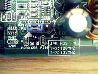
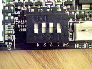
The 100/133MHz jumper on the EPoX 8KTA3
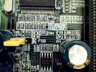
The 100/133MHz jumper on the Iwill KK266
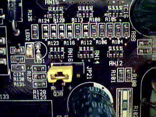
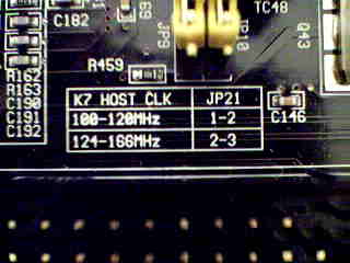
The above two pictures show the 100/133MHz jumper on the AOpen AK73 ProA
VIA claimed that they did not pay any attention to this potential problem because they do not design their reference boards around overclocking. They expected people to stay within the 100MHz FSB range when using an Athlon-B, and only go into the 133MHz range when dealing with the Athlon-C processors.
Avoidance is the Best Solution
One of the most direct solutions to any problem is to avoid it. In this case, that means going with a board that is either fully jumperless or completely jumpered. These boards modify the default multiplier at the same time they set the FSB speed.

Jumperless boards include the ABIT KT7A-RAID and ASUS A7V133. A quick email to ABIT confirmed that the default FSB speed on the KT7A-RAID, before the BIOS is initialized, is 100MHz. The ASUS A7V133 most likely does the same thing.
A fully jumpered motherboard overcomes the “problem” in a similar way since, once again, multiplier and FSB are both set simultaneously - as soon as the board is powered on in this case. So far, thethe ASUS A7V133 and the AOpen AK73 ProA are the only examples of fully jumpered boards. Of course, the ASUS A7V133 can work in either fully jumpered or fully jumperless mode, and that’s why it shows up in both categories here.
We tested this theory on all the above mentioned boards with a 100% success rate on our Athlon 800 (8x100).
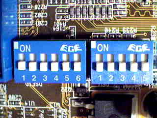


The dipswitches found on the ASUS A7V133 for changing the clock multiplier
The dipswitch found on the AOpen AK73 ProA for modifying the clock multiplier
The Art of Deception
But what happens if you don’t happen to own any of the aforementioned boards? Don’t give up yet; there are still ways to get around the problem. The last resort, of course, is to physically changethe default multiplier, right on your CPU. This is what was required to raise the multiplier when Socket-A overclocking first hit the streets, before the multiplier pins of the Socket-A interface were discovered. The only difference now is that we’re trying to lower the multiplier. Unfortunately, modifying the multiplier of an AMD chip is not exactly the easiest thing to do, but with the help of something we discovered by accident in the early days of Socket-A overclocking, it isn’t quite so bad.
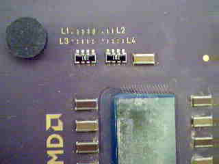
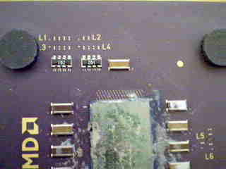
Before jumping into the solution, we have to first revisit the bridges on a Socket-A CPU and see how multiplier ratios are actually set. On any Socket-A chip, you will find three sets of bridges that control the default multiplier relayed to the motherboard: L3, L4, and L6. The L6 bridge refers to the Frequency ID pins (FID) and the L3 and L4 Bridges refer to the BP_FID pins. Basically by manipulating these three sets of bridges, you can change the clock multiplier of the CPU all the way from 5 to 12.5 (in 0.5 increments).
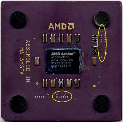
The locations of L3, L4, and L6 bridges on a Socket-A CPU
So theoretically in order to make your chip having a lower multiplier, you just need to follow the Frequency Selection chart in the article from Tom’s Hardware. However, when modifying those bridges, oftentimes the hardest thing to do is to cut one of these bridges. Connecting an already broken bridge is simple enough, since it can be done with a mechanical pencil or a conductive pen. Cutting a bridge can actually be dangerous, as the tools required to do so could actually damage the CPU.
Therefore, the ideal solution would minimize the number of bridges that need to be cut, while at the same time achieving our goal of lowering the default clock multiplier. Back in our AMD Thunderbird / Duron Investigation and Overclocking Discussion, we accidentally thought that the jumpers on the FIC AD-11 were in charge of the FID pins, when in fact they controlled the BP_FID pins. The result of that is we weren’t able to raise the multiplier any higher than the default, even though we could lower the multiplier.
That piece of information gave us a big hint - even if the FID pins and the
BP_FID pins do not match, the chip will still work. So it is possible for us
to modify either set of bridges to lower the multiplier. Since the L6 bridge
controls the default clock multiplier and it has only four pairs, it is the
best candidate for us to play with. Keep in mind that our goal is to let the
chip boot up at a lower multiplier for a few clock cycles so that the settings
from the BIOS come in and take charge.
Digging Deeper
The following diagram illustrates all the combinations of the L6 bridges and their corresponding multiplier values. With the help from DaddyG of the AnandTech Forums we see how the bridges set the multiplier.
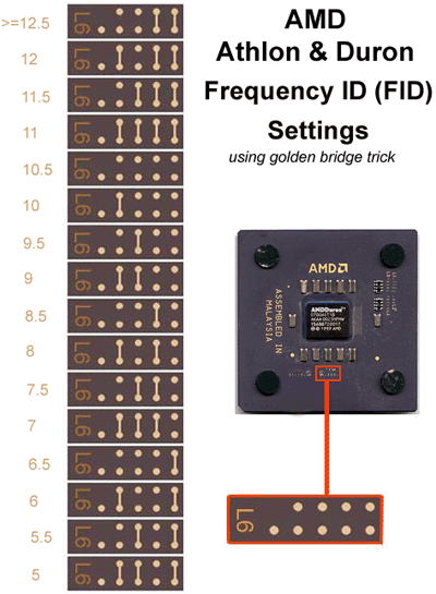
Basically when you look at the L6 Bridge, starting from the end with the extra one dot, the four pairs of bridges correspond to multiplier adder values of 1/2, 1, 2, and 4, which of course is just binary (2^-1=1/2, 2^0=1, 2^1=2, and 2^2=4). Add all the values correspond to open bridges. Then, if the value is between 0 and 1.5, add 11 to obtain the clock multiplier, and if the value is between 2 and 7.5, add 3 to obtain the clock multiplier.
Let’s take our 800MHz Athlon as an example once more. The L6 bridge is shown below. The two open bridges correspond to values of 1 and 4; add them up and you get 5. Since the value is between 2 and 7.5, you add 3 and that’s how the multiplier of 8 is derived.
Since L6 corresponds to FID, and we already know that setting BP_FID below the FID results in a fully functional CPU running at a lower than default multiplier, it is possible that we could only modify the L6 bridge to lower the default multiplier.
In order to prove this theory, we used two AMD chips, one 750MHz and one 800MHz, on the a KT133A board, with the clock multiplier set at default. With the chips untouched, they booted at 750MHz and 800MHz respectively. From the above diagram you can see that the L6 bridges on both 750MHz and 800MHz chips can be modified to that of a 700MHz chip easily by connecting one bridge. When we booted up the system with these chips, both were recognized to have a multiplier of 7 and booted up at 700MHz. The rest of the story is just a matter of choosing the best bridge to modify.
For the sake of saving time we used a pencil to actually make
the connection between the bridges. However as we outlined
in our Athlon Overclocking Guide, we strongly recommend you
use conductive ink or epoxy to make the connections.
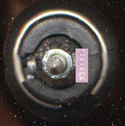
Athlon 750: Notice the pencil mark on the left most L6 Bridge to change the
multiplier from 7.5 to 7
Athlon 750: The L3 and L4 Bridges are left untouched
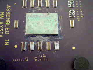
Athlon 800: Notice the pencil mark on the second L6 Bridge from the left. Clock
multiplier changed from 8 to 7
Athlon 800: Once again, the L3 and L4 Bridges are left untouched
Both the modified Athlon 750 and Athlon 800 are booted at 700MHz when the multiplier
on the board is set to default.
Notice that once you past the POST, you can enter BIOS and change the clock multiplier to your desired value, provided that the L1 bridge are all closed. For example, if you intend to run your chip at 7.5 multiplier, but using the method we discussed here the multiplier is changed to 7, you can always boot up your computer at 933MHz (7x133MHz), then enter the BIOS and change the multiplier to 7.5.
If you want to help things along a bit, you can increase the default voltage the CPU will request by modifying the L7 bridges - the easiest is to just connect all L7 bridges, which indicates a voltage of 1.85V. Keep in mind that a normal Athlon has a default voltage of 1.7V and chips of 1GHz and above are set to run at 1.75V, whereas all Durons are set to run at 1.5V.
Unfortunately, certain CPUs will require you to cut a bridge to lower the multiplier, just because of the default multiplier on that particular CPU. One example is the 1.1GHz Athlon, which has a multiplier of 11, meaning that all L6 bridges are closed at the fab. In that case, you are forced to cut one bridge to bring down the clock multiplier.
The Ancient art of Bridge Cutting
We just mentioned that with certain CPUs, such as the 1.1GHz Athlon, all of the L6 bridges are closed at the fab meaning that it is necessary that you cut at least one of the four bridges. But what's the best way to go about doing so? Unfortunately there is no easy way to approach this task, however we have been able to successfully break the L6 bridges on a CPU in the AnandTech lab. Want to know how we did it? Keep on reading but we must warn you, if you wish to repeat this experiment we take no responsibility for anything that may happen to your CPU.
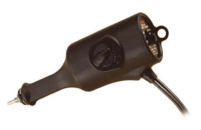
The only tool required for the job is a $20 electric engraving tool that can be found at most hardware stores (see www.dremel.com for more information). We found that this particular tool did the job relatively well, but don't get fooled by that statement. It's still a daunting task.
This brings up the next issue, if you look at the picture below, we have the tip of this electric engraver scanned in at the same resolution as the L4 bridges off of an Athlon CPU. Looking at the tip of the dremel, and the small section of the bridge that must be cut, this is indeed going to be a difficult task.
Trying to break the bridge by just making contact with the electric engraver proved to be one of the less efficient ways of approaching this task. Instead, we set the engraver to its highest speed setting on the dial, and ran it across the area where we wanted to break the bridge. This helped to wear down the bridges and make the process of breaking the bridge much easier.
Then, setting the engraver to a lower speed setting (at the highest speed setting it is difficult to keep steady, this helps somewhat), we lightly tapped the engraver's tip against the bridge we wanted broken until the bridge did break.

The black areas around the L3, L4 and L6 bridges are where the electric engraver was used. For this particular project, we broke all of the L3, L4 and L6 bridges and used conductive ink to connect the ones we needed, thereby making this Athlon 1GHz processor a 750MHz processor that would work at 7.5 x 133MHz (1GHz) on any KT133A motherboard. We actually needed to make this CPU for an upcoming chipset comparison we are working on, more on that later though...
This process requires a lot of patience and you do run the risk of actually damaging the contacts on both sides of the bridge, thus rendering the bridge useless so we do caution you if you wish to proceed using this method: do so at your own risk.
Suggestions and Limitations
So now with the last piece of the puzzle revealed, what’s left is is to figure out what you should do with your specific chip. Keep in mind there are a lot of possibilities, but these are our suggestions for the easiest changes.
Duron 600 and Duron 650
It is actually advisable to try testing the chip directly with 133MHz FSB without modifying the L6 Bridge. Most Duron 600’s and 650’s can hit 800MHz (6 x 133MHz) and 866MHz (6.5 x 133), respectively. If you really have to lower the multiplier, you can add one bridge to Duron 600 or two bridges to Duron 650 to lower the multiplier to 5.
Duron 700 and Thunderbird 700
If you have this chip, it will take quite a bit of work, because it is one of those scenarios where you simply have to cut a bridge. Closing the remaining bridge doesn’t help since you will actually bump the multiplier to 11. What we suggest is to cut the bridge associated with multiplier adder of 2 and add in the bridge for adder 4. This will bring the clock multiplier back to 5, allowing the CPU to boot at 667MHz (5 x 133MHz)
Duron 750 and Thunderbird 750
Start by connecting the bridge corresponding to a multiplier adder of 1/2 and see if the chip boots up at 933 (7 x 133MHz). Most of these CPU’s will be able to obtain such a speed if the voltage is boosted to 1.85V (as mentioned previously). If you’re not so fortunate, consider using the procedure for 700MHz chips from above to bring the multiplier down to 5.5.
Duron 800 and Thunderbird 800
These are similar to 750MHz chips, so try to connect the bridge corresponding to the multiplier adder 1 and see if the chip boots at 933 (7 x 133MHz). Most of these CPU’s will be able to obtain such a speed if the voltage is boosted to 1.85V (as mentioned previously). If it doesn’t work follow the instructions for a 700MHz chip to lower the multiplier to 6.
Thunderbird 850
Connect the bridge corresponding to multiplier adders 1/2 and 1, which will bring the multiplier down to 7. This should allow you to boot at 933MHz (7 x 133MHz), which should work in most cases if the voltage has also been boosted to 1.85V (see above).
Thunderbird 900 / 950 / 1000
The L6 bridges of these chips is actually quite similar to those for 500 / 550 / 600 CPU’s. All you need to do is close the bridge corresponding to adder 4, and that will bring down the clock multiplier from 9 / 9.5 / 10 to 5 / 5.5 / 6, respectively, which is way lower than what you need just to boot.
Thunderbird 1.1GHz
As we mentioned previously, all bridges are closed for a multiplier of 11, so you can’t do anything with this chip unless you cut one of the bridges. If you do choose to cut a bridge, you can cut either the bridge that correspond to adder 2 or the one to adder 4. The first case will bring the multiplier down to 5, and the second case will lower it to 7. Both cases, when booting at 133MHz, will result in clock speed lower than 1.1GHz.
Thunderbird 1.2GHz
Try to connect the remaining bridge to lower the multiplier to 11 and boost the voltage to 1.85V by closing all L7 bridges.. There is a chance that this will not work because you are still trying to boot the chip at 1463MHz (11 x 133MHz), which is more than 200MHz above the 1.2GHz spec, although it may be possible long enough to let the BIOS override to a lower value. If it doesn’t work, follow the instructions for the 1.1GHz, and you should be able to get the multiplier ratio down to 6 or 8.
The above suggestions are just for references. We tried to minimize the number of bridges that had to be modified, especiallythe cutting of bridges. Notice that even in the worst case you will only need to cut one bridge to enable a lower multiplier. If you figure out a configuration that requires cutting two bridges or more, you should re-consider. Of course, this is just a starting point - we just want the system to boot so we can then go in and modify the multiplier in the BIOS. As always, if you don’t have your motherboard already, we recommend the much easier route of just purchasing a motherboard that is fully jumpered or fully jumperless to avoid the whole issue.
Final Words
There is no doubt that the VIA KT133A chipset gives us a lot more flexibility in overclocking thanks to a much wider range of functional FSB speeds. And of course, the performance benefits of the 133MHz FSB cannot be ignored - you get near DDR performance without the need for new memory modules. Unfortunately, all too many motherboards have a problem with overclocking a CPU by lowering the multiplier and simultaneously increasing the FSB, which is exactly what we all want to do to take advantage of the 133MHz FSB of the KT133A. The issue seems to come up on boards that have the multiplier in the BIOS but FSB in jumpers/dipswitches. It also seems to be related to the fact that during the initial boot up, before BIOS settings are loaded, the system looks at the default values to initialize the CPU. That boot up sequence totally defeats the attempt to overclock a 100MHz Athlon/Duron by lowering the clock multiplier and raising the FSB to 133MHz (or higher).
Luckily there are still workarounds for the problem. They range from choosing a motherboard that features a fully jumperless or fully jumpered design to actually modifying your chip to obtain a lower multiplier. Even with the most tedious possibility of modifying the chip, it’s not as hard as what you may expect. In most cases, it is nothing more than adding a few bridges to the chip and, in the worst case, you will have to cut a bridge.
Hopefully this guide gives you a clear explanation of what happened and also the corresponding solutions. As always, great care must be taken when overclocking in general, with extra care taken when modifying any of the bridges on the chip
Last of all, we would like to acknowledge VIA, ABIT, and Iwill for providing us with much of this information, as well as DaddyG from the AnandTech Forums for some of the details on multiplier settings.


