Original Link: https://www.anandtech.com/show/717
ASUS A7V133 Socket-A KT133A ATX
by Mike Andrawes on February 12, 2001 1:45 AM EST- Posted in
- Motherboards
Introduction
The KT133A market is currently one of the most hotly discussed topics in the computer market. With DDR motherboards evolving slowly, the Pentium III sticking to either the Intel i815E or VIA Apollo Pro 133A chipsets, and the Pentium IV not being able to draw much attention, the recent migration from the KT133 to KT133A proves to be the most exciting thing going on right now for hardware enthusiasts.
Over the past two weeks we have looked at KT133A solutions from ABIT, EPoX, and MSI. There is no doubt that they are all good solutions, each with their own unique features, and all of them with impressive performance and stability. One of the reasons for their successes is that the KT133A chipset is extremely similar to the good old KT133 chipset, which is itself virtually identical to the KX133. The result of this heritage is that it has had time to mature and most manufacturers are quite familiar with it by now.
ASUS is the latest manufacturer to bring a KT133A candidate to the AnandTech labs. ASUS has always been one of the most solid and well-respected motherboard manufacturers in the industry, providing high performance, and most importantly, high quality motherboards for all users. One of their more recent successes was the CUSL2, a Socket-370 motherboard that simply stood out from the rest of the crowd with its myriad of features, excellent performance, and rock solid stability..
ASUS’s KT133 solution, the A7V, was quite also an impressive one. With its unique design, the board delivers decent performance and great stability. Although the board didn’t have as many features as some of the other contestants in our last Socket-A motherboard roundup, the A7V was still high on many buyer’s list.
Instead of sitting back and raking in the sales, they decided to learn from others and listen to users to make their next generation board even better. The result is the A7V133. Without further ado, let’s see what ASUS has done and whether this board can stand out from the others.
|
ASUS A7V133 |
|
|
CPU
Interface
|
Socket-A
|
|
Chipset
|
VIA
KT133A
VT 8363A North Bridge VT 686B South Bridge |
|
Form
Factor
|
ATX
|
|
Bus
Speeds
|
90
/ 95 / 100 - 166MHz (1MHz increments)
|
|
Core
Voltages Supported |
Auto Detect 1.10 – 1.85 V (in 0.05V increments) |
|
I/O
Voltages Supported |
3.35
/ 3.56V
|
|
Memory Slots
|
3 168-pin
DIMM Slots
|
|
Expansion Slots
|
1
AGP Slot
5 PCI Slots (3 full length) 1 AMR Slot 0 ISA Slots |
|
On-board Audio
|
VIA
VT1611A AC’97 CODEC
|
|
BIOS
|
Award
Medallion BIOS 6.00
|
|
BIOS
Revision
|
1002A1
(2/5/2001)
|
Still Unique
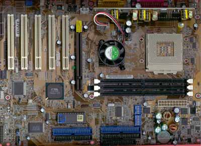
The layout of the A7V133 is more or less the same as the A7V. There are only some minor changes in the choice of components and layout of traces, but it is basically the same. Once again, the most noticeable part of the layout would be the vertically mounted daughterboard next to the I/O panel at the back of the motherboard, which contains quite a few capacitors and power regulators.
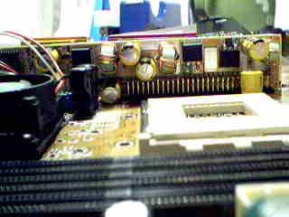
The vertically mounted daughterboard
The advantage of this daughterboard is that the rest of the board is now much “cleaner,” in the sense that there are not as many capacitors on the board as with some other KT133A motherboards. This leaves plenty of space around the CPU socket for you to install a large HSF unit. Our only complaint is that there is a short 820uF capacitor sitting pretty close to the top right hand corner of the CPU socket, which could affect the installation of some extremely large HSF units.
The DIMM slots are located right in front of the CPU socket. Thus ,if all DIMM's are populated with memory, unlocking the HSF unit using a screwdriver as a lever could be a problem unless you remove the memory first.
The power connector is located below the DIMM slots, which ensures that power cables will not have to run over the memory and the CPU, potentially blocking airflow to the CPU. Moreover, just like most other KT133A contenders, the A7V133 is equipped with a full HSF unit on the VIA 8363A North Bridge for better cooling.
Also just like the A7V, we have to complain about the placement of the two IDE connectors provided by the Promise Ultra ATA 100 controller. Since they are located in front of the AGP and first PCI slots, they may get in the way of long AGP or PCI devices on those slots. Careful routing of your IDE cables can usually overcome this oversight by ASUS. Ideally, they would be located in front of the DIMM slots, just like the other IDE and floppy connectors.
One last thing to notice is that the A7V133 is uses a pretty hefty PCB, around 12 by 9.5 inches. Therefore, make sure your case has enough space for the board.
Other than that, the layout is quite good. There is enough space between the DIMM slots and the AGP slot such that you can add or remove memory with an AGP card already in place – something that is unfortunately not possible with many other motherboards.
The Bare Essentials
The VIA 8363A North Bridge sits right between the CPU socket and the AGP Pro slot. It is the core of the KT133A chipset that provides all the major features of the board including official support for 100 / 133MHz FSB and memory buses, as well as AGP 4X support. Just like most of the recent ASUS motherboards, the A7V133 is equipped with an AGP Pro slot. Save for a few very high end graphics cards, the extra power carrying cabilities of AGP Pro are rarely required. The AGP Pro slot is a universal slot, which means it is not keyed specifically for 1.5V or 3.3V cards, so you can install almost any current AGP card in the slot.
The 8363A North Bridge officially supports the 133MHz DDR FSB (266MHz effective), naturally offering support for the new 133MHz FSB Athlons as well. In the past, even with 1GHz Athlons, you were limited to a FSB speed of 100MHz DDR and a multiplier of 10. Now the KT133A chipset allows you to have a FSB speed of 133MHz and possibly higher, so that with the same 1GHz chip, you can lower the multiplier to 7.5, and effectively boost the overall performance while remaining at the same clock speed. This is technically a form of overclocking, but is probably the safest form possible.
Most of the recent AMD Socket-A motherboards have included the hardware mechanism for changing the multiplier ratio settings of AMD processors, so this can be done easily. There is some effort required on your part to prepare your CPUs for overclocking, however we have diagrammed exactly what is necessary in our Athlon Overclocking Guide. Make sure you read the guide in order to fully unleash the power of your Socket-A processor.
Just like most other KT133A solutions, the A7V133 features a total of three DIMM slots, supporting up to 1.5GB SDRAM. The memory controller in the 8363A North Bridge allows you to run your memory at either 100MHz or 133MHz, depending on your FSB choice. When running a 100MHz FSB, you have the option to choose 100MHz or 133MHz memory operation. However, at 133MHz memory speed is always synchronous. Officially the KT133A chipset only supports FSB:memory ratios of 100:100, 100:133, or 133:133.
The newer VIA 686B South Bridge has replaced the good old VIA 686A South Bridge that was used on most KT133 boards. The advantage of the 686B over 686A is that it supports Ultra ATA 100, whereas the 686A only supports Ultra ATA 66. The Ultra ATA 100 controller provides two IDE channels that support up to 4 IDE devices (two per channel).
Two traditional USB ports are mounted at the back of the motherboard together with the serial / parallel ports, and there are connectors ready for a third and fourth USB port at the left side of the board. Luckily enough, when you purchase the A7V133 you will get the necessary USB bracket to take advantage of the second USB controller. Unfortunately, unlike the A7V, ASUS does not feature the of the on-board Alcor Micro AU9254 USB Hub that offered another three USB connectors. Therefore the A7V133 “only” features four USB ports, as opposed to the seven of the A7V. ASUS still retains the silk screen on the A7V133 for the Alcor Micro USB Hub, so if there is a need ASUS can always add the chip back or even make it an optional feature.
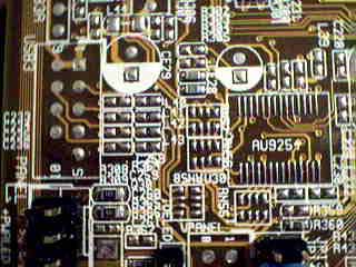
The silk screen for the Alcor Micro chip and the USB connector.
The 5/1/0/1 (PCI/AGP/ISA/AMR) expansion slot design, although not ideal, should be more than enough for most users. For those who still want to keep some of their ISA devices, the A7V133 is just not going to be the right choice. Although the overclocking market is growing rapidly, ASUS is still one of the largest supporters in the OEM market, which is still the source of the majority of their sales. Therefore, keeping the AMR slot helps OEMs provide a low cost modem solution for end users.
This time around, ASUS decided to add in onboard audio, using the VIA VT1611A for AC’97 audio CODEC. On the A7V, this was an option that was usually only found in OEM versions of the board. Once again, AC’97 audio is capable of providing basic sound for some users, but for anything more, you really should go with a hardware-based PCI sound card. ASUS also has a version of the A7V133 without on-board audio, which should bring down the price of the board slightly.
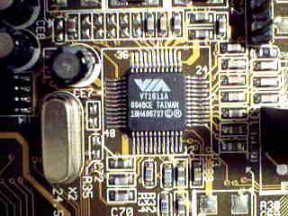
VIA VT1611A CODEC
On par with ABIT and MSI
One of the complaints we had about the ASUS A7V was that changing the multiplier had to be done using dipswitches, whereas ABIT and MSI allowed that to be done in the BIOS. The ability to make such adjustments in the BIOS definitely helps make things easier for overclockers since they can do all overclocking in the BIOS, without having the hassle of turning off the power, modify the dipswitches, and reboot.
Now with ABIT, EPoX, and MSI all having the setting implemented in the BIOS, ASUS can’t afford to fall behind on this one. Therefore with the A7V133, you are allowed to modify the multiplier ratios from within the BIOS as well, provided that your have your AMD CPU is unlocked already. The values range from 5 to 12.5 in 0.5 increments, which is the same range we’ve seen on all KT133/KT133A motherboards with this feature.
ASUS has keept all the dipswitches on the motherboards, in case some users still prefer this type of overclocking. There is a jumper where you can choose to use the JumperFree mode or the Jumper mode. When you choose the JumperFree mode, all the FSB speed, multiplier ratio, and CPU core voltage settings are selected from within the BIOS. Otherwise you will use four jumpers to set the CPU core voltage, and two sets of dipswitches to select the multiplier ratios and a selected set of FSB speeds.
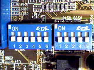
The two sets of dipswitches.
If you use the dipswitches for setting the FSB speed, your choices are limited to 100 / 103 / 105 / 110 / 133 MHz, which is not even close to the amount of settings a real overclocker would want. On the other hand, under the JumperFree mode, you can choose from 90MHz, 95MHz, or any value between 100 – 166MHz in 1MHz increments. As we have seen numerous times before, the lack of 1MHz increments in FSB speeds almost always ends up being the bottleneck in overclocking a CPU to its absolute maximum speed.
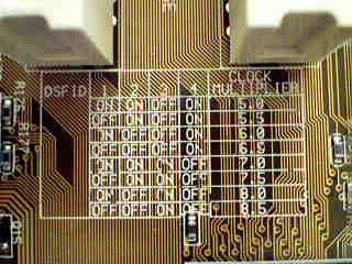
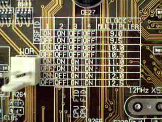
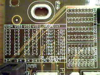
The most important part of the manual is printed on the board as well
Unfortunately, there is no jumper to choose from the 100MHz range or the 133MHz range as in the case of EPoX and MSI, which should make overclocking much easier. As we mentioned, in general the KT133A chipset allows the CPU:Memory ratio of 100:100, 100:133, and 133:133. With the A7V133, it works like this: if you choose an FSB speed between 95MHz and 120MHz, you will have the option to run your memory at either the FSB speed or the FSB speed plus the PCI speed. Notice that the PCI speed is not always 33MHz as you vary the FSB speed. For example, if you set the FSB speed to 110MHz, the choices for memory bus are either 110MHz or 146MHz, which means the PCI bus is running at 36MHz. When it is at the 120MHz limit, the choices are either 120MHz or 160MHz, which means the PCI bus is running at 40MHz. Starting from 121MHz FSB speed, the memory bus is locked at the same speed as the FSB speed, and you will lose the privilege of running your memory at a faster speed.
For I/O voltage, there is a jumper on the motherboard where you can choose from 3.35 or 3.56V. From our experience we still haven’t seen any scenario where increasing the I/O voltage actually helps overclocking, but it’s always nice to have this kind of tweaking just in case it comes in handy.
Showing the Improvements
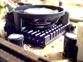
As we mentioned before the A7V133 is equipped with a complete HSF unit on the 8363A North Bridge for better cooling. Based on previous experience, this HSF unit is a specially designed one for better airflow. As you can see from the pictures, one side of the fan unit is left open, so when the unit is working, the air is blowing towards the bottom left corner. This way the heated air from the North Bridge would be blown towards the video card and the memory instead of the CPU, which may lower CPU temperatures slightly. Unfortunately, ASUS did not put any thermal compound between the HSF unit and the North Bridge, something that all other manufacturers have done with the KT133A boards we have seen..

From CPU: It is well covered.
From AGP slot: It is wide open
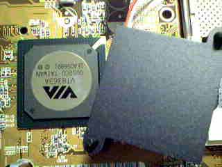
No thermal compound between the HSF unit and the North Bridge.
The A7V133, just like the A7V, uses the Award Medallion BIOS 6.00, which closely resembles an old Phoenix BIOS setup, except that it has more performance tweaking features, especially with regards to memory. For the A7V133, there are quite a few tweaks you can do to the memory timing, including (but not limited to) CAS latency, RAS Recharge time, and RAS to CAS latency.
There are a total of four fan headers on the board, one for the CPU HSF, one for the North Bridge HSF, and two extra headers for chassis fans. Just like other ASUS motherboard, hardware monitoring is provided by a custom ASUS AS99127F ASIC that can monitor three temperatures, three fan speeds, and six voltages.
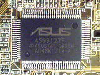
ASUS AS99127F ASIC.
The A7V was very highly recommended, partly because of its incredible stability. If you recall, during our 24-hour Content Creation Winstone 2000 stress tests the A7V crashed a total of two times, which was very impressive since the normal crash rate was around five times. For the A7V133, ASUS modified several things in order to keep up with the faster FSB speed. For starters some of the traces have been changed in order to provide cleaner signals and sustain the faster speed. On the other hand, besides the several 680uF and 820uF capacitors, ASUS also put in several larger 1500uF capacitors around the CPU socket, North Bridge, and DIMM slots.
With these little adjustment, ASUS was able to make the A7V133 even more stable than the A7V. Running at 133MHz FSB, the A7V didn’t crash once at all, matching the MSI K7T Turbo. We continued the stress tests on the A7V133 and tried to see if it crashed within 48 hours, and it didn’t happen here either. So in terms of stability, ASUS took yet another step , putting them neck and neck with MSI.
The A7V is equipped with the Promise Ultra ATA 100 controller, which provides two Ultra ATA 100 IDE channelsInstead of using the Promise PDC20265 chip on the A7V, ASUS chooses to use the Promise PDC20265R chip on the A7V133 as a second Ultra ATA 100 IDE controller. The difference between the two chips is that the PDC20265R on the A7V133 supports RAID 0 configuration. Interestingly, RAID 1 and RAID 0+1 are not supported on the A7V133, despite the fact that this chip does in fact support these modes on other motherboards. Since the chip clearly supports the feature, it has probably been disabled in the BIOS, which means that we can hope for a future BIOS update to re-enable the feature. Also interesting is the fact that ASUS actually uses a jumper to select standard ATA 100 operation or RAID 0 operation - most other boards with the Promise controller handle all of this in the BIOS.
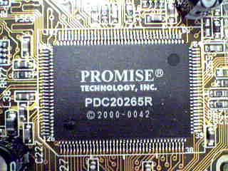
Promise Ultra ATA 100 IDE RAID controller.
The ASUS manual is always famous for the amount and information included, and that unparalleled quality is carried on to the one included with the A7V133. It includes virtually all the information you would need for the motherboard, including instructions on how to install the motherboard, details on all the BIOS settings, IRQ sharing, jumpers and connectors settings, BIOS flashing, drivers / utilities installation, and more.
What's the redline?
When we were reviewing KT133 motherboards, we found out that 115MHz was the maximum a KT133 motherboard could sustain, with 110 MHz a much more reasonable limit. Since FSB overclocking was not that useful, we figured that it would be interesting to see how much we could overclock a CPU by changing the multiplier and then the FSB, since multiplier overclocking proved to be more effective.
However, with the KT133A chipset, FSB overclocking is worth a closer look with the new official support for 133MHz FSB operation. With the KT133A chipset, we are sure that FSB speeds of up to 133MHz are no longer a problem, but we decided to find out how high above 133MHz can we push the FSB speed.
To do this, we took a 1GHz Athlon processor, a Mushkin PC133 CAS2 PC133 SDRAM, and a NVIDIA GeForce2 GTS as our test bed. We started the testing by setting the 1GHz CPU to run at 133MHz FSB, thus a multiplier ratio of 7.5. Then we gradually increased the FSB speed and ran tests to make sure the system was stable at that speed. If needed, we also tried to set the CAS latency to 3 and all other memory timings to as slow as possible, so that the PC133 SDRAM would not be the limiting factor. Moreover, when the CPU speed got to high, we lowered the multiplier ratio setting so that the clock speed of the CPU remained close to 1GHz.
For our testing, initially with CAS2 and normal memory settings, the highest FSB speed we achieved was 145MHz. At that speed we could still run SYSMark 2000, Quake III Arena, and Content Creation Winstone 2000 with no problem. However, setting the FSB speed to 146MHz the system couldn’t boot at all. This value is slightly higher than the one achieved by the ABIT KT7A-RAID and the MSI K7T Turbo.
We then lowered the CAS setting to 3 and reduced any other memory related settings in the BIOS, allowing us to get the FSB up to 148MHz and ran all the tests with no problem. At 149MHz, the system could not boot again. This result is also slightly higher than the one achieved by ABIT and MSI
Like what we have mentioned in the previous reviews, 148MHz is around a 10% overclock from 133MHz - the same percentage increase we had with the KT133, so this is no major surprise.
Still ASUS
We did have a few complaints regarding the otherwise well made board.
For starters, the two IDE connectors from the Promise controller would be better placed in front of the DIMM slots, so that they would not block the placement of some longer AGP or PCI devices.
ASUS still doesn’t implement any jumper for clearing the CMOS. Therefore, if you have to clear the BIOS, you will have to use a screwdriver to short two specific solder points.
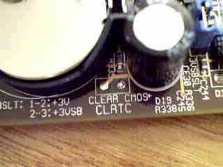
There is no jumper to clear CMOS.
The expansion slot design is not the best in the world with only five PCI slots and no ISA slot, but it should be sufficient for most users.
Finally, it would be great if ASUS had included some thermal compound on the HSF unit for the North Bridge to improve cooling a bit.
The Test
In recent times, choosing a motherboard cannot be completely determined by a Winstone score. Now, many boards come within one Winstone point of each other and therefore the need to benchmark boards against each other falls. Therefore you should not base your decision entirely on the benchmarks you see here, but also on the technical features and advantages of this particular board, seeing as that will probably make the greatest difference in your overall experience.
Click Here to learn about AnandTech's Motherboard Testing Methodology.
|
Test Configuration |
|
| Processor(s): |
AMD
Athlon (Thunderbird) 1GHz
|
| RAM: |
1 x 128MB Mushkin PC133 SDRAM
|
| Hard Drive(s): |
Western Digital 153BA Ultra
ATA 66 7200 RPM
|
| Bus Master Drivers: |
VIA 4-in-1 v4.24 Service Pack
|
| Video Card(s): |
NVIDIA
GeForce 2 GTS 32MB DDR
|
| Video Drivers: |
NVIDIA
Detonator 5.22
|
| Operation System(s): |
Windows
98 SE
|
| Motherboard Revision: |
ASUS
A7V133 Revision 1.04
|
|
Windows 98 Performance |
|||
|
Athlon 1GHz OEM |
SYSMark 2000 |
Content Creation Winstone 2000 |
Quake 3 Arena 640x480x16 |
|
ASUS A7V133 (KT133A / 133MHz) |
197 |
37.6 |
153.4 |
|
MSI K7T Turbo (KT133A / 133MHz) |
194 |
37.5 |
145.7 |
|
EPoX EP-8KTA3 (KT133A / 133MHz) |
196 |
36.7 |
146.3 |
|
ABIT KT7A-RAID (KT133A / 133MHz) |
197 |
37.4 |
149.6 |
|
MSI K7T Pro2 (KT133 / 100MHz) |
189 |
35.8 |
135.1 |
Things get quite interesting with the results on the A7V133. The ABIT KT7A-RAID doesn’t hold the performance crown anymore, as it is edged out ever so slightly by the A7V133. We can see that the SYSMark 2000 and Winstone 2000 scores are still very close to each other, but in the Quake 3 Arena tests, the A7V133 jumped out with a 5% lead over the MSI K7T Turbo, mostly due to its more flexible memory tweaking options.
In general, we are still looking at a very mature series of motherboards. There should be some more room in performance with future BIOS updates, but from the fact that most scores are packed closely together, we can expect such performance boosts to be minimal.
Final Words
The A7V133 is yet another impressive KT133A motherboard. It has some solid performance numbers, and its stability with the MSI K7T Turbo is outstanding. The improvement from just a Promise Ultra ATA 100 controller to a controller with RAID 0 support will definitely attract more users. Last of all, the inclusion of multiplier ratio settings in the BIOS, as well as 1MHz increments in FSB speeds settings helps ensure that the A7V133 is as user-friendly as the other KT133A candidates.
On the other hand, there are still things that ASUS could have done better. Among them is the placement of the two IDE connectors by the Promise controller, which will block the placement of any long AGP or PCI devices. Moreover, the implementation of RAID 0 (striping) but not RAID 1 (mirroring) for the Promise controller seems to be an odd choice as well, since the controller should be capable of both, as shown by its use on the MSI K7T Turbo.
Being the fourth KT133A solutions we reviewed, we are really impressed by what manufacturers have done. They have gone much further than just swapping in the VIA 8363A North Bridge for the older 8363 North Bridge, but they have improved stability and added features as well. There are still several KT133A motherboards on the way, and we will continue to bring you coverage of as many boards as we can get a hold of.
How it Rates
|
AnandTech Motherboard Rating |
|
|
Rating (x/10)
|
|
|
Performance
|
8.0
|
|
Price
|
6.0
|
|
Stability
|
9.5
|
|
Quality
|
8.0
|
|
Features
|
7.0
|
|
Layout
|
5.5
|
|
Availability
|
7.0
|
|
Documentation & Software Bundle
|
7.5
|
| Overall Rating - not an average Click here to find out why |
8.5
|

