Original Link: https://www.anandtech.com/show/7034/computex-2013-asrock-z87-with-22-sata-ports
Computex 2013: ASRock Z87 with 22 SATA Ports [Update]
by Ian Cutress on June 7, 2013 10:00 PM EST- Posted in
- ASRock
- Motherboards
- Trade Shows
- Z87
- Computex 2013

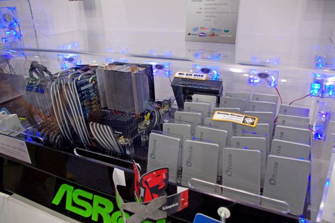
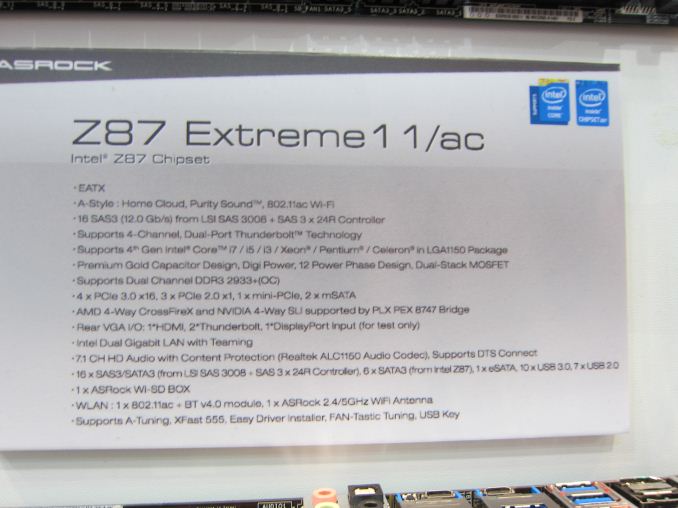
For X79 and Z77 ASRock have released an Extreme11 model, known for being high price due to the integrated PLX and LSI 2308 RAID chips to provide extra PCIe lanes and eight more SATA ports. For Z87, ASRock have gone one step further – the Extreme11 for Haswell will be four way SLI and Crossfire capable, but with an LSI chip designed to handle 16 SAS/SATA ports:
We get six SATA 6 Gbps from the chipset, and 16 from the LSI chip. If these were all SATA 6 Gbps, then we might expect a maximum peak speed in RAID-0 of 11 GBps, pushing the bandwidth of what I would assume is the PCIe 3.0 x8 required for the LSI chip harder than ever before. But the peak speeds showcased by ASRock were half this value at 5.5 gigabytes per second, suggesting that these LSI ports may be SATA 3 Gbps limited. Unfortunately I did not take a picture of what LSI chip was on board, although it does say SAS3 capable, which makes me wonder if it is not the 2308 or one that splits the SATA 6 Gbps into two SATA 3 Gbps.
I did ask about how many PLX chips were onboard – I was told one, which would suggest 32 lanes total when used in the normal configuration. This would mean that 4-way SLI and the LSI chip would not be possible, unless used in an abnormal configuration, such as the EVGA Z77 FTW which allocated only 8 lanes to the PLX to split into 32, and then we would have the other 8 for the LSI chip.
No word on price or release date yet (it is not on their website), but I could imagine it might be hitting the $600 of the Z77 Extreme11, although that had an additional PLX chip. The extra cost of the newer LSI chip might counterbalance this.
Update:
After speaking with ASRock and a few emails back and forth, we have some more information. I was particularly concerned about the PCIe lane allocation, and how to organize a single PLX 8747 chip for all the lanes involved. Most regular readers of our motherboard reviews will recognize that the PLX 8747 chip takes in up to 16 PCIe 3.0 lanes from the CPU and outputs 32 PCIe 3.0 lanes using a multiplexing technology and buffers (as we explained here).
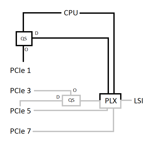
ASRock uses a combination of switches and the PLX chip to achieve four-way SLI capablility and supply enough PCIe lanes to the LSI 3008 chip (confirmed):

In the diagram above, each line represents 8 lanes, and QS stands for Quick Switch which has a default path and an optional path (the optional path is used when a card in that slot is in use).
This means the following:
In single GPU use, we put the PCIe card in PCIe 5 for x16 lanes from the PLX which at this time has an x16 uplink to the CPU.
In dual GPU use, we put the cards in PCIe 5 for x16 lanes from the PLX and PCIe 7 for x8 lanes from the PLX. The PLX in this mode has an x16 uplink to the CPU.
- Alternatively we could put our cards into PCIe 5 and PCIe 3 for x8 lanes each from the PLX – the PLX in this mode has an x16 uplink.
- OR we could put our cards into PCIe 1 for 8 lanes from the CPU and PCIe 5 for 16 lanes from the PLX, with the PLX only having an x8 uplink.
In tri-GPU use, we can put the cards into PCIe 3, 5 and 7 for x8 lanes each from the PLX, meaning the PLX has an x16 uplink.
- OR we could put the cards into PCIe 1 for x8 from the CPU, PCIe 5 for 16 lanes from the PLX, and PCIe 7 for 8 lanes from the PLX. The PLX in this mode would have an x8 uplink.
- OR we could put the cards into PCIe 1, 3 and 5 for x8 (CPU), x8 (PLX), x8 (PLX), with the PLX having an x8 uplink.
In quad-GPU use, we only have one option:
- PCIe 1 has x8 from CPU
- PCIe 3 has x8 from PLX
- PCIe 5 has x8 from PLX
- PCIe 7 has x8 from PLX
- PLX has x8 uplink
Personally this is a very complicated way of doing this, and I find it a little frustrating.
I offered ASRock the following alternatives (where PEG 1 and PEG 2 are 8 lanes from the CPU):
PEG 1 to LSI
PEG 2 to 8747 -> x16 to PCIe 1 (switch x8 to PCIe 3) and x16 to PCIe 5 (switch x8 to PCIe 7).
1-way GPU might be slightly different (due to x8 uplink limitation).
OR:
PEG 1 to PCIe 1
PEG 2 to 8747 -> x8 to LSI, x8 to PCIe 1 (switch to PCIe3), x8 to PCIe 5, 8x to PCIe 7
This would give x16 to one PCIe (8x via PEG, 8x via PLX) with one GPU, x16/x8 in dual-GPU, x16/x8/x8 in tri-GPU and x8/x8/x8/x8 in quad-GPU.
Nevertheless, the lane allocation is now set for the Extreme11 as the one in the diagram. Other new information on the board is that ASRock are using the LSI 3008 eight port SAS chip with an LSI 3x24R expander to give 16 SAS ports with a max uplink speed equivalent to eight ports (hence the 5.5 gigabytes per second read/write speed).
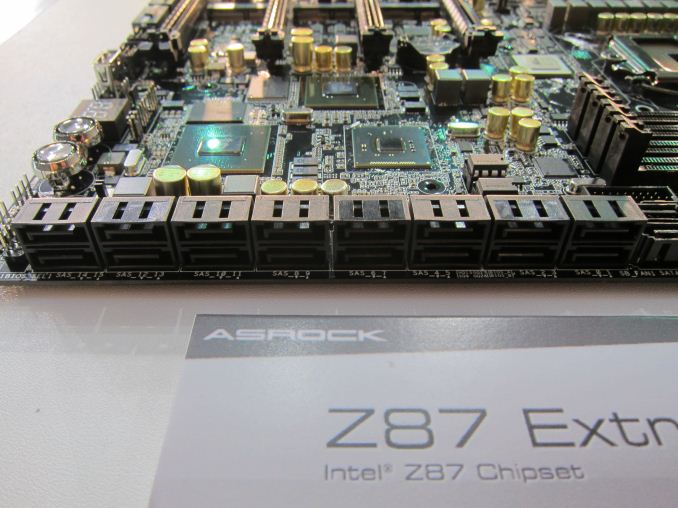
Many thanks to one of our readers clille who was able to take some extra pictures of the motherboard:


