Original Link: https://www.anandtech.com/show/6790/intels-clover-trail-dualcore-cpu-and-graphics-unveiled-at-mwc-2013
Intel's Clover Trail+: Dual-Core CPU and Graphics Unveiled at MWC 2013
by Anand Lal Shimpi on February 25, 2013 12:00 AM EST- Posted in
- Intel
- Atom
- Trade Shows
- SoCs
- Clover Trail+
- MWC 2013
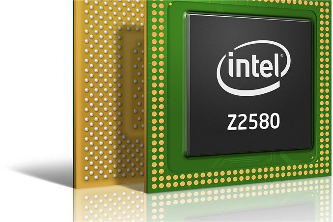
We find ourselves at another Mobile World Congress, discussing another Intel Atom based smartphone SoC. While last year we were talking about faster and lower performing versions of the Medfield family, this year there’s a new topic for discussion: Clover Trail+.
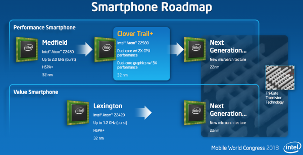
Here’s where Intel’s codenames start getting a bit confusing. Medfield was the original 32nm Atom SoC for smartphones, while Clover Trail was the 32nm platform for Windows 8 tablets. Clover Trail+ is still a 32nm Atom based SoC but it can be used in phones and tablets.
Architecturally, Clover Trail+ takes the Medfield platform, adds a second CPU core (and leaves Hyper Threading enabled), dramatically improves GPU performance and introduces the same memory controller enhancements that were present in the original Clover Trail. Compared to Clover Trail, CT+ mostly adds improved graphics performance.
Intel Goes Dual-Core
On the CPU side we’re still talking about 32nm 2-wide in-order Atom cores, with two threads per core (4 threads total per chip). This is still a direct descendent of the original 45nm Atom core that first debuted in 2008. Intel is quick to point out that the redesigned 22nm architecture is still on track for an introduction (in tablets) this holiday season, but for now we’re still stuck with the old core.
That’s not to say that 32nm Atom isn’t competitive. As we’ve already shown, from a performance standpoint the 5 year old Atom architecture is still faster than everything but ARM’s Cortex A15. Qualcomm’s 28nm Krait architecture is lower power, but Intel is at least competitive.
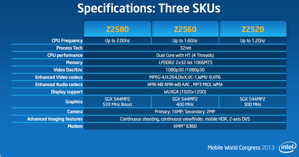
Frequencies vary depending on the SKU you’re talking about. Just like with Medfield, there are three CT+ SKUs: the Atom Z2580, Z2560 and Z2520. Compared to the previous generation the second digit has been incremented by one indicating that CT+ is obviously newer/better.
All three SKUs feature two cores, but what changes is their max CPU and GPU clocks. the Z2580 tops out at 2.0GHz, just like the Z2460 does today. The Z2560 hits 1.6GHz, and the Z2520 runs at up to 1.2GHz. Both cores are capable of these peak frequencies. The low and nominal operating frequencies are all listed in the table below:
| Intel Clover Trail+ SoC Lineup | |||||||
| Intel Atom Z2580 | Intel Atom Z2560 | Intel Atom Z2520 | Intel Atom Z2460 | ||||
| CPU Cores/Threads | 2 / 4 | 2 / 4 | 2 / 4 | 1 / 2 | |||
| CPU Max Turbo Frequency | 2.0GHz | 1.6GHz | 1.2GHz | 2.0GHz | |||
| CPU Max Non-Turbo Frequency | 933MHz | 933MHz | 933MHz | 900MHz | |||
| CPU Low Frequency Mode | 800MHz | 800MHz | 800MHz | 600MHz | |||
| L2 Cache | 2 x 512KB | 2 x 512KB | 2 x 512KB | 512KB | |||
| Memory Interface | 2 x 32-bit LPDDR2-1066 | 2 x 32-bit LPDDR2-800 | |||||
| Display support | 1920 x 1200 | 1024 x 768 | |||||
| GPU | PowerVR SGX 544MP2 | PowerVR SGX 545 | |||||
| GPU Max Turbo Frequency | 533MHz | 400MHz | 300MHz | 533MHz | |||
| Baseband Pairing | XMM 6360 | XMM 6260 | |||||
Single threaded CPU performance should remain unchanged from Medfield, but multi/heavily-threaded workloads will see a healthy boost running on Clover Trail+.
A Much Faster GPU
The big change is of course the GPU core. While Penwell SoC in Medfield integrated a single PowerVR SGX 545 core, CT+ features two PowerVR SGX 544 cores. The SGX 544 looks a lot like the SGX 543 used in Apple’s A5/A5X, but with 2x the triangle setup performance and DirectX 10 class texturing hardware. There’s no change to the shader ALU count:
| Mobile SoC GPU Comparison | |||||||||||||
| PowerVR SGX 543MP2 | PowerVR SGX 543MP4 | PowerVR SGX 544MP2 | PowerVR SGX 554MP4 | ||||||||||
| Used In | A5 | A5X | CT+ | A6X | |||||||||
| SIMD Name | USSE2 | USSE2 | USSE2 | USSE2 | |||||||||
| # of SIMDs | 8 | 16 | 8 | 32 | |||||||||
| MADs per SIMD | 4 | 4 | 4 | 4 | |||||||||
| Total MADs | 32 | 64 | 32 | 128 | |||||||||
| GFLOPS @ Shipping Frequency | 16.0 GFLOPS | 32.0 GFLOPS | 34.1 GFLOPS | 71.6 GFLOPS | |||||||||
As always, Intel is very aggressive on GPU frequencies in CT+. The 544MP2 runs at a max of 300MHz in the case of the Z2520, and can burst up to 533MHz in the case of the Z2580.
This max frequency can give the Z2580 similar shader performance to Apple’s A5X, and competitive performance to Apple's iPhone 5/A6 SoC. Intel claims GLBenchmark 2.5 Egypt HD offscreen performance somewhere around 30 fps, putting it near the performance of Qualcomm’s Adreno 320.
The CT+ memory subsystem is still a 2 x 32-bit LPDDR2 interface operating, but max data rate moves up to 1066MHz. Putting that sort of GPU power in a mobile SoC is almost unheard of from Intel, and it’s a very good thing to see.
Other Improvements & Power Consumption
Power consumption shouldn’t be any different than Medfield under light CPU loads, however if you keep both cores pegged you’ll obviously burn through your battery quicker. The same is true for the faster GPU. Like many modern smartphone SoCs, the addition of extra cores simply increases the dynamic range of SoC power consumption. Intel does claim that its CT+ FFRD uses less power at idle than Motorola's RAZR i (based on Medfield), although that may be more attributable to the platform itself rather than specifically the SoC. I can see CT+ devices delivering similar battery life, and perhaps even better than Medfield, but I can also see them being a lot worse depending on usage model.
Related to the GPU improvements is ultimately the change that gives CT+ its name. Like Clover Trail before it, the CT+ silicon integrates an updated memory controller that’s capable of some form of reordering of memory operations to allow the GPU to better preempt the CPU when it needs the bandwidth. This change wasn’t present in Medfield but made it into Clover Trail, and is also included in CT+.
The improved GPU also enables support for higher resolution panels, now up to 1920 x 1200. You can already see the higher res display support at work in Lenovo’s IdeaPhone K900 which features a 5.5” 1080p panel, but Intel told us to expect Android tablets based on CT+ as well. Given Intel’s relative absence from the Android tablet space, it’s clear that this is a big deal.
Video encode/decode hardware is mostly unchanged, as are the platform’s capabilities of 1080p30 encode and decode. Intel does claim video decode performance is improved, partially due to the enhancements on the memory interface side.
The Silicon Hive (now owned by Intel) ISP is physically the same as what was in Medfield, but features largely re-written firmware to improve performance and add functionality. Intel improved HDR processing performance with the fw re-write, which is supposed to reduce ghosting and motion blur when shooting in HDR mode. The new firmware also enables support for a time shift mode where you can take multiple captures and select faces from individual frames to assemble a multi-person photo where everyone is smiling/not-blinking.
CT+ still supports up to a 16MP primary camera and up to a 2MP secondary camera, with an 8MP limit for burst mode.
The Baseband Story: Finally XMM 6360
On the baseband side, Intel is finally updating its very old XMM 6260 silicon to XMM 6360. The update brings 3GPP release 9 support, with 42Mbps DC-HSPA+ (Category 24) support, as well as HSUPA category 7 (11.5 Mbps). The XMM 6360 still ships with a pentaband transceiver. While this is still shy of enabling LTE, for many of the world markets where dual-carrier support is important this is a huge step forward for Intel in the baseband department - finally bringing the company up to our baseline expectations.
Intel remains behind Qualcomm when it comes to baseband silicon and it took an absurd amount of time to move off of 6260 for its high end solution. I’m not entirely sure what’s taking so long with modernizing Intel’s modem roadmap but it’s been pretty embarrassing thus far. The good news is we’re supposed to see Intel’s first LTE solution by the end of the year. XMM 6360 is built on a 40nm process, ironically enough not at Intel’s own fabs - a remnant of the old Infineon business that Intel acquired a few years back.
An Updated Reference Design
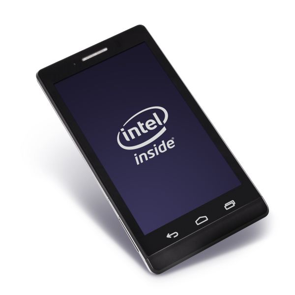
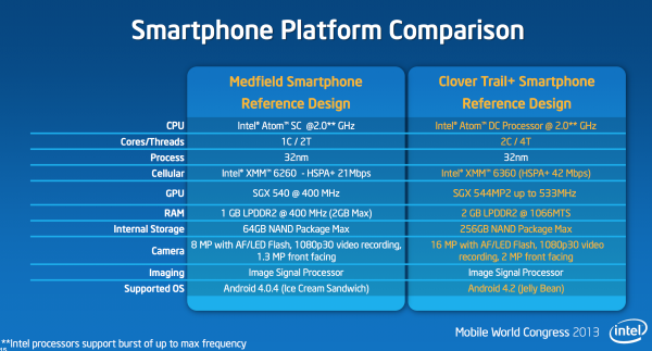
Intel built a new FFRD (Form Factor Reference Design) around CT+, with some obviously updated specs. The new FFRD includes an Atom Z2580 with the new XMM 6360 baseband silicon.
Internal memory gets an upgrade from 1GB of LPDDR2-800 to 2GB of LPDDR2-1066. The maximum amount of NAND supported moves to 256GB, although I’d be very surprised to see that deployed in a shipping device. The rear facing camera module in Intel’s CT+ FFRD moves up to 16MP, while the front facing module gets an upgrade to 2MP.
Finally, the CT+ FFRD ships with Android 4.2.
As always, Intel’s partners are welcome to ship a skinned version of the FFRD if they would like, or they can choose to implement individual components.
Final Words
Clover Trail+ is an important step forward for Intel as it finally shows real progress in the company prioritizing GPU performance. We thought Medfield was a completely acceptable smartphone SoC platform, and was actually very well implemented in Motorola's RAZR i, so it's likely that we'll be similarly pleased with CT+.
Where Intel needs to deliver however is on two fronts. For starters, it needs to bring 22nm silicon to market so we can really see what Intel can do on the power/performance front rather than continuing to have this discussion about Intel simply being within the right range of competition. Secondly, and equally important, is the fact that Intel simply needs more high-profile design wins. Motorola's RAZR i and Lenovo's IdeaPhone K900 both seem like good attempts, but to really begin to pull from Qualcomm it needs Nexus 4, Galaxy S and HTC One class design wins. That, I suspect, is a much more difficult thing to pull off - at least until 22nm silicon rolls around.

