Original Link: https://www.anandtech.com/show/6360/asus-f2a85v-pro-review-a-look-at-fm2-with-a85x
ASUS F2A85-V Pro Review: A Look at FM2 with A85X
by Ian Cutress on October 10, 2012 11:20 AM EST- Posted in
- Motherboards
- Asus
- Trinity
- FM2
- A85X
The new release of Trinity processors on the desktop opens up a cascade of issues when it comes to choosing a new motherboard for your Trinity system. The main point of confusion comes in the face of chipsets, whereby multiple sockets and processor families can use the same chipsets and each motherboard manufacturer has a different naming scheme in order to differentiate the two. Both Intel and AMD have been guilty of this in the past, but in the past 18 months we had no real cause for concern - until now.
The Confusion
From the beginning, let us lay down a few facts on PC components. When a user buys a processor, the design of that processor and the pin layout determines the socket for that processor. Thus if I purchase an i7-3960X today, I know that it will fit into Socket 2011 based motherboards - similarly with the i5-2500K, it will fit into Socket 1155 motherboards. Out of the motherboards that have this socket, two main avenues are available to decide which model is suitable - the chipset, and the additional functionality.
With AMD and socket AM3+, we had choices of the 990FX, 990X and 970 chipsets. With Sandy Bridge there was P67, H67 and Z68 with some extra business level chipsets, and Ivy Bridge gets Z77, H77, B75 and others. The beauty of Sandy Bridge and Ivy Bridge is that all the consumer level chipsets are interchangeable and with BIOS updates, all motherboards in that space will work with both processors. I know that if I buy any Z68 motherboard I can fit either my Sandy Bridge processors or Ivy Bridge processors in them.
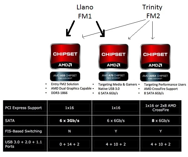
Trinity and the FM2 socket turn the above situation on its head, so to speak. If I went out and bought a Llano processor on an FM1 socket, I have a choice of either A55 or A75 chipsets. However, for FM2, I have a choice also of A55 or A75, alongside the newer A85X chipset. This means I cannot blindly look at the chipset just for a particular processor socket - it also means that motherboard manufacturers have to be static and clear with their naming structure to avoid confusion. But then again, each manufacturer has a different naming structure, which serves to confuse even more.
In terms of naming strategies, the major motherboard manufacturers have the following scheme:
ASUS: F2A85-V Pro - the initial F2 is for Trinity
Gigabyte: F2A85X-UP4 - the initial F2 is for Trinity
ASRock: FM2A75 Pro4 - the initial FM2 is for Trinity
MSI: FM2-A85XA-G65 - the initial FM2 is for Trinity
ECS: A85F2-A Deluxe - First chipset, then FM2 socket
Zotac: A75-ITX WiFi - No mention of FM2 (as per what was shown at Computex)
Biostar: A75MH2 - No direct mention of FM2 (again, from Computex)
So the key is to look for F2 or FM2 on most of the motherboard manufacturers. Failing this, look for the A85X chipset (such as the Biostar HiFi A85X) which should be specifically for FM2 and Trinity processors.
With the naming side of things out of the way, it is important we know how each chipset differs in its functionality. This is primarily summed up in the image above - the newer A85X chipset boasts eight SATA 6 Gbps ports native to the chipset. This is a key differentiator in the AMD vs. Intel battle over chipsets, with Intel only supporting two SATA 6 Gbps (and four SATA 3 Gbps) as native. Complimentary to this change, A85X also supports RAID 5, whereas A75 does not. This opens up low powered Trinity units, with onboard graphics, for use in what I would call 'typical SOHO' NAS environments - no discrete GPU with RAID 5 for redundant storage capabilities.
Also worthy of note is the graphics side of the motherboards we will be testing as part of our Trinity coverage. On A55 and A75, we are limited to a single x16 PCIe 2.0 according to the official documentation - this is despite that A75 on Llano allowed x8/x8 functionality as shown by our review of the ASRock A75 Extreme6 at launch. Whether this is a minor change for FM2 to drive users to Trinity or something else, I am not sure. However, moving to A85X does allow for a rated discrete dual x8/x8 lane allocation.
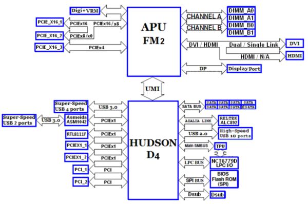
The board we are looking at today has come with a very handy chipset diagram to show exactly what is going on:
Normally on the Intel side of things, we see four lanes of PCIe 2.0 being exposed by the chipset, which would lead to x16/x4 or x8/x8/x4 lane allocations, with that final x4 lane being crippled both by the chipset routing and the bandwidth. However when it comes to Trinity, we actually have 20 PCIe 2.0 lanes coming from the APU to power PCIe devices. This gives each board using an FM2 APU the ability to do at least x16/x4 or x8/x8/x4 (with A85X) without the cripple we see with Intel. In Intel's variation, we saw Crossfire work but SLI not, due to the odd combination of SLI certification required. Chances are that if we do see SLI certification on an FM2/A85X product, then this x4 should be included, though it will be crippled if bandwidth is an issue.
One thing also to note is the lack of PCIe 3.0 functionality. AMD have had PCIe 3.0 enabled video cards for a while now, and the specification has been done and dusted for even longer. Given that the move from Llano to Trinity was an architecture jump (Stars to Piledriver modules), one would expect the shift to have occurred at this point. But for now we are still 'limited' to PCIe 2.0. I use quotation marks on the basis that for most users the jump from PCIe 2.0 to PCIe 3.0 has no influence on normal settings, but for some extreme and limited cases, PCIe 3.0 can help. There is a chance that PCIe 3.0 could be part of the new architecture, but disabled until the next family of processors are launched on FM2. Failing that, FM3 will be a more likely stomping ground for PCIe 3.0. We may have to wait until the APUs use GCN rather than VLIW-4 for their graphics cores.
With all this being said, let us move on to the first of our FM2 and Trinity reviews, with a look at the A85X chipset in the form of the ASUS F2A85-V Pro.
ASUS F2A85-V Pro Overview
The first review using a new processor family and a new chipset family is often difficult. The problem is multi-faceted in the sense that knowledge of a platform is often less than ideal, and the final outcome and conclusion of the board could be tainted by the processor or APU performance in comparison to previous chipsets. This is doubly compounded for this review, whereby for the first time in a long time we are dealing with a middling performance processor (in the absolute sense) in comparison to anything previous over the past 12 months. Since our last foray into this space with Llano and Zacate, our benchmark suite has changed for the most part (such as GPU testing at 2560x1440), but there are some common tests from which we can draw conclusions. Also worth noting is that the first review of a new chipset often leaves few comparison points to be made to the rest of the motherboards in that chipset, given no testing has been performed on the others.
Nevertheless, ASUS did send us the F2A85-V Pro and overall impressions with the motherboard itself are positive. Power delivery heatsinks are sufficient for the Trinity platform, but bolstered by heatpipe connections to the chipset heatsink. Despite the numerous SATA and USB ports offered by the chipset, the board offers an additional ASMedia USB 3.0 controller with the board to take advantage of UASP protocols in USB 3.0 throughput. The board also comes with ASUS Digital Power Delivery options (DIGI+) for CPU and memory, should that be of use to the user for pushing the limits of the board or keeping power consumption down.
Connectivity on the board gives us access to PS/2, USB 2.0, all four common video outputs (VGA, DVI-D, HDMI, Displayport), eSATA, USB 3.0, gigabit Ethernet and PCI connectors on board. Memory is connected via T-Topology rather than Daisy Chain, which in principle should aid in four DIMM memory overclocking. The main areas ASUS like to push with their products is the software, such as Network iControl for program priority of networking traffic, and Fan Xpert 2 which gives the user complete control of all the fan headers (five) on board through the OS including auto tuning. We also get three-way PCIe device functionality onboard, and access to ASUS' USB BIOS Flashback, which allows updating the BIOS via USB without a CPU, memory or video card connected.
Downsides are few, though I would like to know why the single sided latch system ASUS put on their Intel boards for memory is not present here. In the box I would have liked to have seen a front facing USB panel, though as time goes on we only seem to find this in products with two USB 3.0 headers on board. From a personal perspective, I enjoy having a two-digit debug in order to diagnose motherboard issues but ASUS have instead put onboard their Q-LED system which indicates where in the POST process there are issues (while nice, I do not find it fine-grained enough). In a similar ilk, there are no power/reset buttons on board, but like the two-digit debug, these have very few roles when the system is in a case and working smoothly.
Performance wise, it is hard to get past the performance of the Trinity when compared to Ivy Bridge and the like. From a practical standpoint, the lack of floating point units in the CPU gives cause for concern as not everyone codes in hex or integer style (my own personal software all uses FP – INT would be confusing to code for me for negligible gain on most architectures). As this is the first FM2 board we are testing, there are very few comparative conclusions we can draw of the board compared to the competition. We can say that ASUS are still pushing their USB 3.0 boost which gives some distinct read/write improvement numbers, but the copy times for both chipset based and controller based USB 3.0 ports are not as good as Intel offerings. One point of concern is the DPC latency, which for this product jumped around from ~100 microseconds to 600+ microseconds. Usually these jumps are attributed to monitoring software, however there was none loaded into the system. The DPC test should ideally score less than 200 microseconds, but under 500 microseconds is still a pass – for the F2A85-V Pro to score worse than 500 is a little disappointing if audio processing is the main reason to purchase this product. I suspect this could be fixed with a minor BIOS update.
Visual Inspection
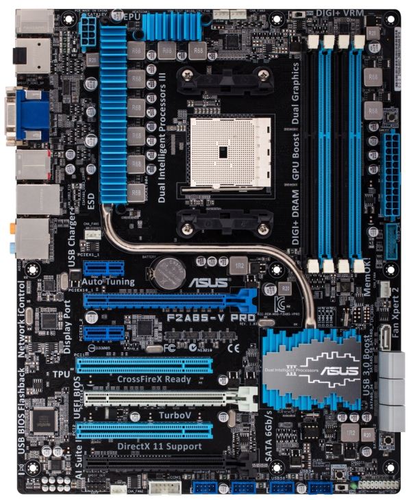
I will be blunt as well as fair - in my opinion, mid range boards seem to lack a level of aesthetic finesse that we get with higher end products. Case in point, I recently fitted a new $100 micro ATX board into my brothers new machine and it was not as pretty as the equivalent high end model I had in my machine. We see something of this mid-range aesthetics on the ASUS F2A85-V Pro. This is by no means negative, but on the higher end niche products, the handling and feel of the PCB just seems cleaner and more efficient, presumably due to consolidation of some of the onboard chips through a higher budget. It is an interesting point to consider. Despite this, everything that can be brought down gratis from the higher end models will end up in the mid range (routing, BIOS, efficiency).
With the F2A85-V Pro we have a standard AMD sized socket for the processor, which in comparison to the competition is a large area to set aside for the processor and a hangover from AM2 requirements. As processors become more efficient, I would like to see AMD redesign the socket area for efficiency and size, which will allow motherboard manufacturers more real estate and room to innovate in the area. Nevertheless, due to the size of the power delivery heatsinks there is plenty of room for even the beefiest air coolers on this motherboard - at a stretch (without directly testing due to lack of equipment), it could be possible that Noctua NH-D14 users may be limited in memory module space with the first slot being covered.
The socket area has four fan headers within easy reach - two 4-pin headers above the socket (one CPU, one chassis), a 4-pin chassis header underneath the power delivery to the bottom left, and another 4-pin chassis header below the USB 3.0 header to the right of the board. The final 4-pin chassis header is found at the bottom of the board next to the onboard audio.
Along the right hand side, the first feature of note is the MemOK! Button - a handy device useful if you set the memory too high. I use it quite regularly when pushing the memory in conjunction with a CPU overclock. Underneath we get the 24-pin ATX power connector, a USB 3.0 header (from the chipset), a fan header, then our SATA ports. As the AMD A85X chipset allows up to eight SATA 6 Gbps ports, chances are we will only see extra SATA controllers on a motherboard if the controller affords special functionality. ASUS have decided to directly use seven ports on this side of the board, with the eighth port being the eSATA port on the IO panel. These SATA ports are capable of RAID 0, 1, 5 and 10. Following this is the BIOS Flashback button on board (rather than an IO panel button as seen on previous iterations).
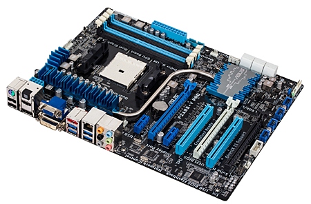
The chipset heatsink covers the A85X chip, which according to specifications can consume up to 7.8 watts. With this heatsink being connected via heatpipe, the main function is to aid in the power delivery cooling, even if the heatsink design does not seem to maximize surface area.
On the bottom of the board are various ports available from use. From left to right we get the front panel audio, a 4-pin fan header, a COM header, four USB 2.0 headers, the TPU switch and then the front panel header. The PCIe layout is reasonable for a two way GPU setup with room for either a PCIe x1, PCI or PCIe x4 card. From top to bottom we get a PCIe x1, PCIe x16 (x8 in dual), x1, PCI, x8, PCI, x4.
One extra switch on the board is related a lot to the first Intel X79 board I reviewed. On that board we were given a switch on the IO panel that when activated would send the user to the BIOS on the next boot. We have a similar technology here on the F2A85-V Pro in the form of a DirectKey button above the TPU switch along the bottom. When pressed in the OS, it will shut down the system and on the next boot go straight into BIOS. When pressed if the system is off, it will start up the system and boot into the BIOS. This is highly useful for overclockers and reviewers such that we do not have to hold down the Del button on boot to access the BIOS. This is not an ASUS specific feature for FM2 and A85X as I have seen it on other products, but I reckon it is a good feature to have nonetheless, even if it seems odd to include it without having power/reset buttons or a Debug LED.

The rear IO panel gives us PS/2 functionality in a combination port, two USB 2.0 in black, optical S/PDIF output, all four VGA outputs (HDMI, DP, D-Sub, DVI-D), eSATA 6 Gbps (in red), four USB 3.0 (in blue, two from an ASMedia controller, two from chipset), gigabit Ethernet (Realtek 8111F) and audio jacks (Realtek ALC892).
Board Features
| ASUS F2A85-V Pro | |
| Price | Link |
| Size | ATX |
| CPU Interface | FM2 |
| Chipset | AMD A85X |
| Memory Slots |
Four DDR3 DIMM slots supporting up to 64 GB Dual Channel, 1066-1866MHz |
| Video Outputs |
VGA DVI-D HDMI DP |
| Onboard LAN | Realtek 8111F |
| Onboard Audio | Realtek ALC892 |
| Expansion Slots |
1 x PCIe 2.0 x16 (x8 in dual) 1 x PCIe 2.0 x8 1 x PCIe 2.0 x4 2 x PCIe 2.0 x1 2 x PCI |
| Onboard SATA/RAID |
7 x SATA 6 Gbps (FCH), RAID 0, 1, 5, 10 1 x eSATA 6 Gbps (FCH) |
| USB |
4 x USB 3.0 (FCH) [2 back panel, 2 onboard] 2 x USB 3.0 (ASMedia) [2 back panel] 10 x USB 2.0 (FCH) [2 back panel, 8 onboard] |
| Onboard |
7 x SATA 6 Gbps 1 x USB 3.0 Header 4 x USB 2.0 Headers 1 x COM Header 1 x Front Panel Audio 5 x Fan Headers 1 x MemOK! Button 1 x USB BIOS Flashback Button 1 x DirectKey Button TPU/EPU Switches Q-LED |
| Power Connectors |
1 x 24-pin ATX Power Connector 1 x 8-pin CPU Power Connector |
| Fan Headers |
1 x CPU (4-pin) 4 x CHA (4-pin) |
| IO Panel |
1 x PS/2 Combination Port 1 x VGA 1 x DVI-D 1 x HDMI 1 x DP 2 x USB 2.0 2 x USB 3.0 (Chipset) 2 x USB 3.0 (ASMedia) 1 x GbE (Realtek 8111F) 1 x Optical S/PDIF Output Audio Jacks (Realtek ALC892) ` |
| Warranty Period | 3 Years |
| Product Page | Link |
The F2A85-V Pro currently retails at launch for $140, which is around $20 more expensive than the most powerful FM2 processor. This price comparison usually means that the board should provide all the functionality a user would need. So our limitations to Realtek audio and NIC is more due to the fact this is AMD rather than Intel (Gigabyte could call on Atheros for their products), though the decision to use an ALC892 rather than the ALC898 is a little odd. Perhaps dual NIC would have been nice, or the fact that the Pro board in Z77 has the combination WiFi/Bluetooth module on board makes me wonder how much of a price increase that would have caused for a product like this.
ASUS F2A85-V Pro BIOS
The ASUS BIOS is one that we have come to know and enjoy using, given its simplicity and ease-of-use. Over my tenure at AnandTech I must have covered at least ten different Intel based ASUS BIOSes, but only one ever AMD ASUS BIOS. Today we raise that figure to two with the F2A85-V Pro. Despite this, users of Intel based ASUS graphical BIOSes will not see much difference visually to the Intel counterparts.
In terms of performance, the only issues I really had with the BIOS were temperature readings and memory settings. The former is due to this weird thing that AMD processors seem to do – only show temperature values between 25C and 60C. In the operating system this means that even if you ramp up the voltage, all of the temperature reading software sees values in this range. Normally while overclocking I like to keep an eye on temperatures, in case they start hitting a limit. 60C is still fairly cool in overclocking scenarios, so I was surprised when I could keep ramping up the voltage with no discernable affect. It could be a case of other software needing to hook better into the temperature sensors, but even ASUS’ own temperature control was showing this. I personally found it a bit odd. Regarding memory settings, we have options to set from default all the way up to DDR3-2400 MHz, and the processor is rated up to DDR3-1866 by AMD specifications – the system would randomly decide if DDR3-2400 was stable during testing, and as a result some of the initial tests were at 2400, and the rest are at 2133. This is either indicative of the motherboard, or indicative of the memory controller in these processors not being geared to 2400 MHz (or I have a dud of a sample). The last thing about performance I would like to mention is our voltage readings in OCCT, which were fairly erratic. However I will cover that later in the review.
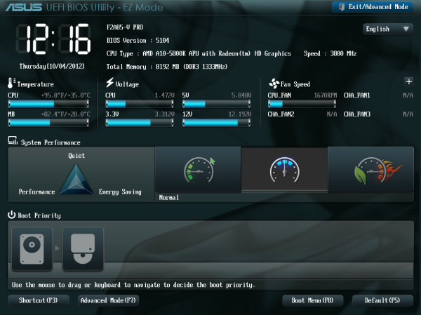
For the BIOS itself, our first screen presented is our easy mode:
This screen has the majority of what we want when a user opens a BIOS – the name of the motherboard being used, the BIOS version, the CPU installed (with speed), memory installed (with speed), voltage readings, temperature readings, fan speed readings and a boot priority order. I am very glad I have all of this to hand and it is easy to see. The additions I would suggest are by having some of the objects clickable to various advanced options located deeper in the BIOS – such as clicking on the ‘Fan Speed’ heading takes us to the fan speed selection. Now clearly ASUS’ way of showing a BIOS is different to that of other manufacturers that use an image of the motherboard as their front end BIOS screen and ask users to click on various parts to access settings. The main difference between the two is essentially whether the companies want to decide if the user is interfacing with a product or a system, and whether that company wants the user to recognize this fact or not. For an average user, obviously interfacing with the system as a whole makes much more sense – they are not too concerned if they are speaking with the motherboard, the CPU, the fan controllers or anything like that. Some enthusiasts however would prefer the acknowledgement that they are talking or manipulating component A or component B within a system. ASUS take this knowledge on board, and let the user interact with the whole of the product from the get-go without confusing users about where the SATA ports actually are.
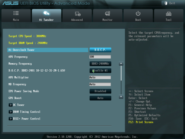
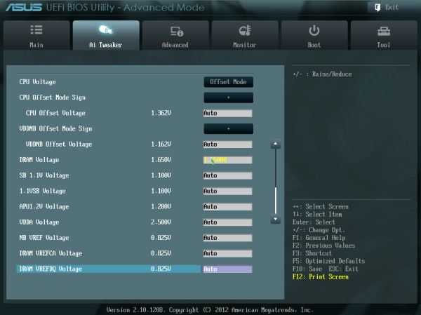
The main screen in the BIOS is the AI Tweaker section, designed to help users overclock the processor. Our overclocking results are shown in our typical overclocking section, but it is important to note that for most overclocking scenarios for the user, all we need to do is adjust voltage and CPU frequency. In the F2A85-V Pro, our first option is to select what type of overclocking we want – Auto (none), Manual, or D.O.C.P. We have encountered D.O.C.P. before on AMD boards, and the quick explanation is ‘a BIOS hack to get XMP to work’. Remember that XMP is an Intel standard, so these motherboard manufacturers have worked out a way to parse that information in an AMD system. By selecting DOCP, the system will adjust the memory ratio, the APU frequency (if required) and the memory sub-timings/voltages to the XMP profile of the kit. In some circumstances this may produce a CPU overclock, so ensure that that CPU frequency is where you would want it as well.
Selecting Manual for our overclock gives us options to adjust the APU Frequency (i.e. the BUS speed / BCLK), the memory frequency, the APU multiplier, the NB Frequency, EPU Power saving modes, and the GPU frequency. Each option has an associated explanation on the right hand side telling the user of what the option does and what values are applicable. Underneath these settings are the ASUS OC Tuner (which applies a fast overclock), our DRAM timing screens, DIGI+ Power control and voltages.
The main voltages for the APU can be adjusted either by an offset or as an absolute value – the rest are changed via absolute values.
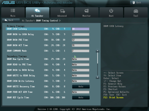
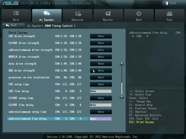
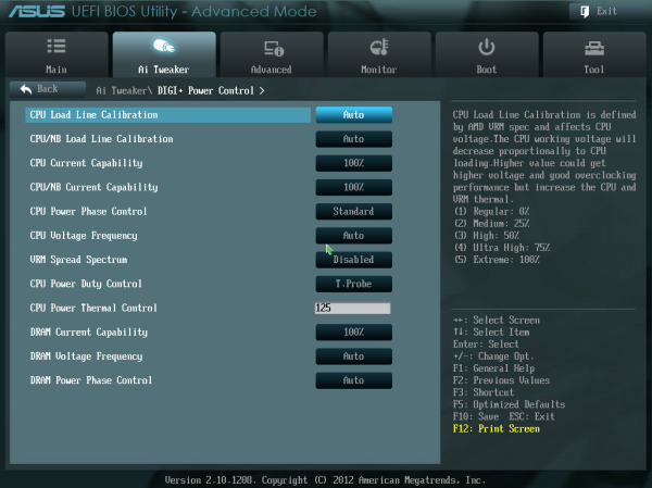
Shots of the Memory and DIGI+ sections:
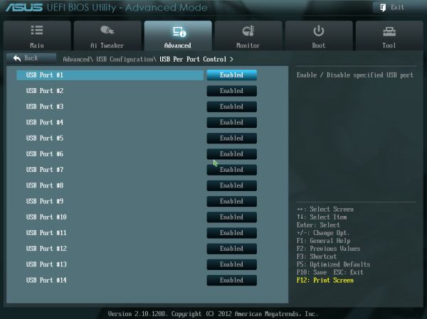
Also in the BIOS are our advanced options which give access to the CPU, SATA, USB, NB and onboard devices. By default our SATA ports are on AHCI which is good, but it is also important to note that each USB port on board can be enabled and disabled through these options:
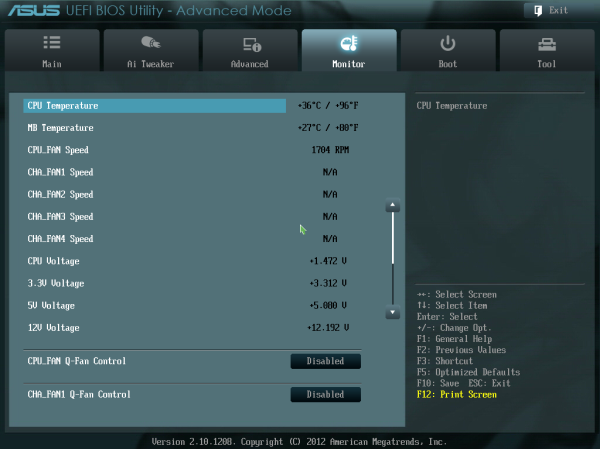
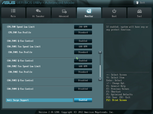
Fan controls are situated in the Monitor section of the BIOS, where this area also shows the important temperatures, fan speeds and voltages. Each of the fan headers on the F2A85-V Pro can be controlled independently, and ASUS give us the option of a low speed limit and a profile to select aggressiveness in the ramping of the fans. The OS software is a lot better to use for fan control than the OS options in this regard.
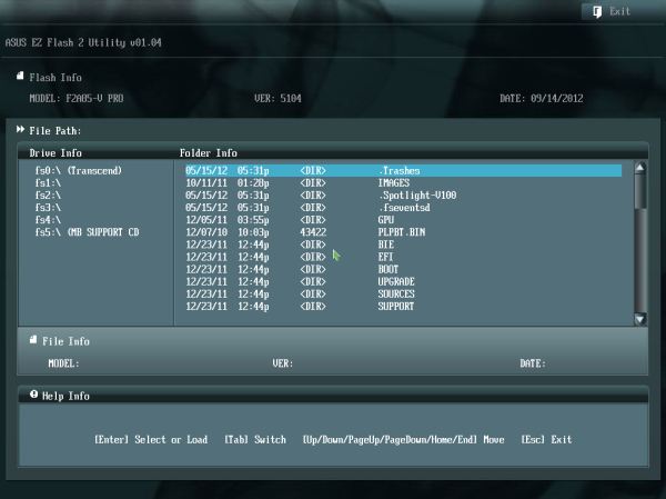
Also in the BIOS we have the EZ-Flash utility for updating the BIOS, SPD information to confirm the memory is the memory purchased, and an option to save up to eight OC profiles.
ASUS F2A85-V Pro Software
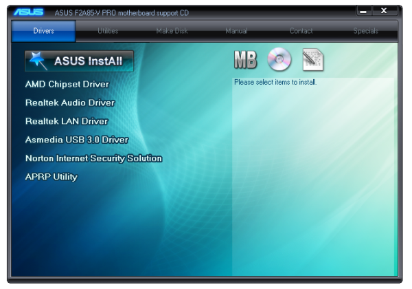
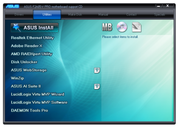
The software package provided by ASUS is often cited by us as one of the best software packages with a motherboard, and this is still true on the FM2 socket and Trinity processors. The install CD is the same platform used by ASUS on their Intel products, with one menu for software and another for utilities. Each of these menus allows for a one-click ‘Install-All’ option, and clicking through allows users to deselect certain options that may not be relevant to them.
Within the software package, Daemon Tools Pro was installed by default. I have used Daemon Tools for years – it is a great piece of software for mounting disk images.
The main software package revolves around ASUS’ AI Suite. This software acts as an interface for the smaller additional programs that ASUS create for use on the motherboard.
ASUS AI Suite
The main bar of AI Suite splits the sub-programs up into groups, with two of the major utilities having their own buttons. In the case with the F2A85-V Pro this is the Auto Tuning option for overclocking and the Remote Go utility for media and file organization over network connections to tablets and smartphones. We will go through these in turn.
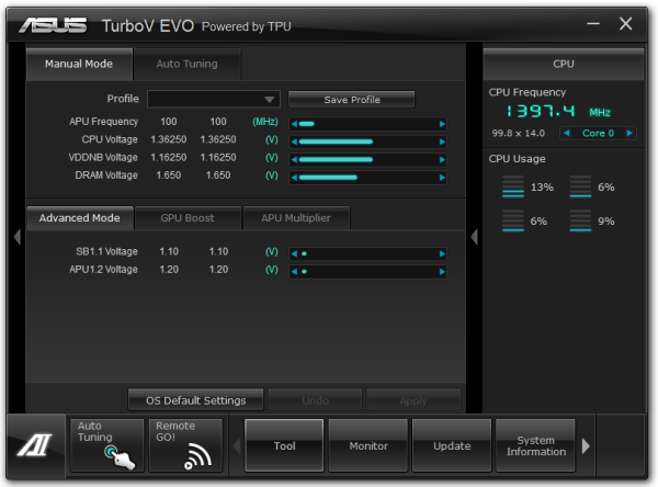
TurboV Evo
TurboV Evo is the operating system based overclocking tool provided. It allows for changes of all the important voltages and frequencies onboard, as well as providing the Auto Tuning options for ‘Fast’ and ‘Extreme’ overclock settings. I usually find TurboV Evo a good bit of kit when overclock testing, though I would like to put in some values by numbers rather than having to fiddle with sliders all the time.
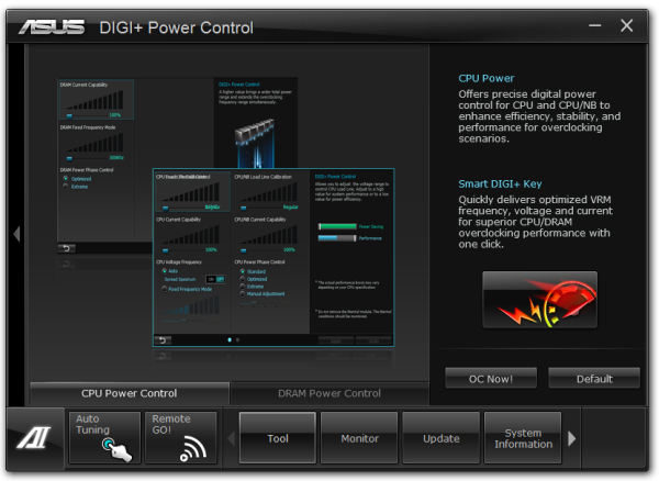
DIGI+ Power Control
In order to give users better control over the power delivery, ASUS implements their DIGI+ Power Control on the FM2 boards as well. There are fewer options here than on some of their higher end Intel board offerings, but if a user wants to give more current capabilities or adjust load line calibrations through the OS for overclocks, the options are here for both the CPU/APU and the DRAM.
In a similar vein, we also have the EPU (Energy Processing Unit) menu and settings, designed to adjust and power gate different parts of the motherboard to save energy.
Fan Xpert 2
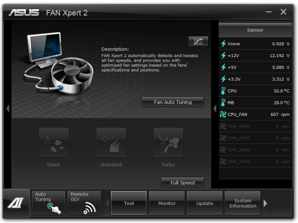
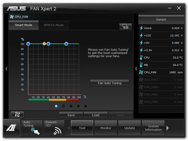
ASUS are well known in the motherboard space for using better fan controllers that the rest of the motherboard industry – typically one per fan header which is configurable within the BIOS and in software. The beauty of these fan headers lie in their independent control – the system has access to the RPM output and can adjust the speed on the fly. Pair that up with some software that actually can manipulate such a system and we have a nice fan configuration. The software behind this is Fan Xpert 2 – bundled as part of AI Suite, it will test all the fans in the system and provide RPM vs. Power applied graphs (as this relationship is rarely linear). This allows users to adjust the temperature/RPM curves as required – the only thing missing is the ability to apply hysteresis.
USB 3.0 Boost
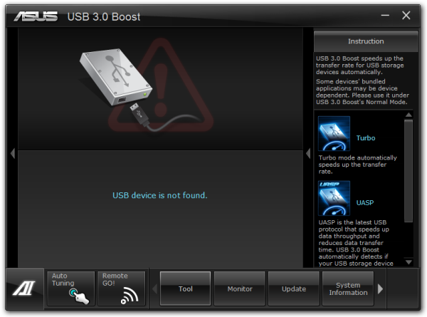
As part of the ASUS methodology, we have onboard an ASMedia controller which can take advantage of the most up to date USB 3.0 transfer protocols. By attaching a compatible USB 3.0 device, and a click of the USB 3.0 Boost interface, the software will apply a driver over the standard ASMedia driver in order to enforce these under the hood commands. As we have shown in previous reviews, this affords a nice bump in the speeds provided at low transfer size workloads, making a USB device more tenable for everyday random access use rather than just storage. USB 3.0 Boost can also apply a modified driver to the chipset USB 3.0 ports for a similar boost using BOT protocols rather than UASP. (Note, this should become moot for Windows 8, where UASP will be a part of the standard driver package.)
Network iControl
For the past couple of years it has been clear that users in the motherboard industry would prefer the ability to manipulate the network ports onboard their system. While doing some epic downloading while playing a twitch FPS online is a little bit of an odd combination, using software tools in the OS to manage the priority of these programs is never a bad thing. On the ASUS side this comes in the form of Network iControl, and within this software the user can adjust the software that uses the Ethernet connections and rank them in order of priority. Alternatively the system can be left on automatic, and the program will use a series of pre-defined rules to prioritize a lot of the well known programs that typically rely on low-latency throughput.
Elsewhere in AI Suite we have advanced charging software in the form of AI Charger+ and USB Charger which will manipulate the current output of specific USB ports if the appropriate device is connected. This will help greatly with charging devices, using up to 1.5A rather than 300mA. I have been asked to test this feature in future reviews, and when I have an accurate setup I will start to test these charging features. Specifically AI Charger+ is for Apple products, and USB Charger is for other devices (Kindles, smartphones et al.).
ASUS also use their USB BIOS Flashback software here, allowing users to update the BIOS without having a CPU, Memory or VGA connected. This is a feature that helps protect the product in case new CPUs are released and microcode updates are needed. If a user buys a board that is not compatible with their processor, in the past an older processor had to be found in order to update the BIOS. This is no longer the case with USB BIOS Flashback.
ASUS F2A85-V Pro In The Box
What we get in the box usually is the cream of the package - something that little bit extra that makes the whole product a more enjoyable experience. Despite this, the price of the board usually indicates what level of goodies we get in the box, even if we have had a few surprises in the past. With this product selling for $140 at launch, more expensive than the high end Trinity processors, we should feel that there's something in the box to make it worth while. What we actually get in the box is:
Driver CD
IO Shield
User Manual
Four SATA Cables
Q-Connectors
The box could be a little more filled with joy - either a USB 3.0 panel or something similar. As mentioned before, I would have liked to see the ASUS WiFi/Bluetooth module on the 'Pro' board, which would have included antenna and the module in the box.
Voltage Readings
[retracted]
Unfortunately we are unable to bring you the results of our OCCT test, due to a level of incompatibility between OCCT and current FM2 boards we have discovered that was not correctly reading the voltage. This test in the future will require an OCCT update.
ASUS F2A85-V Pro Overclocking
Experience with ASUS F2A85-V Pro
Overclocking on a new platform is always a little frustrating – even if the principles of overclocking have not changed, or the architecture has not changed, a manufacturer may slightly confuse with different names for voltages, and there is no experience guiding how these processors may interact under voltage.
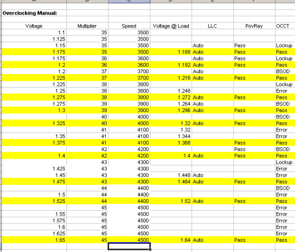
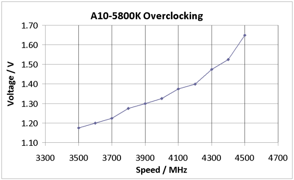
As such we have to take a methodical view to overclocking. For almost all 24/7 CPU overclocks all we ever need to adjust is the CPU multiplier and the CPU voltage, so starting with the load multiplier and voltage that comes with the processors is never a bad thing. In the case of our test bed we had an A10-5800K which has a maximum turbo multiplier of 42x and a load voltage of around 1.40 volts according to OCCT. Using this information I performed overclock testing starting at an underclock of 35x and attempted to find the minimum voltage needed to be set in the BIOS to make this stable. The system was then raised slowly with the multiplier, each time finding the minimum voltage required to be stable.
The third option that an overclocker may play with is Load Line Calibration. This adjusts the voltage drop across the processor when under load (as causing the processor to do work causes a droop in the voltage reading) – a low LLC uses less energy overall in the system and is often dictated in part by the processor manufacturer. However a high LLC often has the benefit of making an overclock stable. In the case of ASUS motherboards we get a variety of options for LLC, but for the purposes of testing here it was left on automatic.
The experience of overclocking on the F2A85-V Pro was fairly standard for a top tier motherboard – we get two automatic overclock options in the OS in the form of ‘Fast’ and ‘Extreme’, as well as one in the BIOS and the TPU switch on board which both perform the ‘Fast’ overclock. Manual overclock involves either playing with the AI Suite software until the system is unstable, then making permanent adjustments in the BIOS as required. Without comparing against other motherboards yet I cannot say how well this board performs relative to others, but having the temperature reading issue does not help much.
Methodology:
Our standard overclocking methodology is as follows. We select the automatic overclock options and test for stability with PovRay and OCCT to simulate high-end workloads. These stability tests aim to catch any immediate causes for memory or CPU errors.
For manual overclocks, based on the information gathered from previous testing, starts off at a nominal voltage and CPU multiplier, and the multiplier is increased until the stability tests are failed. The CPU voltage is increased gradually until the stability tests are passed, and the process repeated until the motherboard reduces the multiplier automatically (due to safety protocol) or the CPU temperature reaches a stupidly high level (100ºC+).
Our test bed is not in a case, which should push overclocks higher with fresher (cooler) air. We are using a beQuiet Dark Pro CPU cooler with its stock fan. This is a high-end air cooler, designed to tackle up to 150W of CPU power without issue.
Automatic Overclock:
Using the AI Suite software, we navigated to the TurboV Evo Automatic Tuning menu. It offers two options – ‘Fast’ and ‘Extreme’. Here are our results with these options.
With the ‘Fast’ option, the system rebooted indicating the CPU had been boosted to 43x and 100 MHz (4300 MHz total), with the IGP also boosted to 950 MHz. This overclock passed both OCCT and PovRay.
With the ‘Extreme’ option the system rebooted and initialized stress testing with the processor. The software started adjusting the CPU multiplier in the OS, rebooted then adjusted the APU frequency. When all was said and done, the final result was a CPU overclock to 44x and 100 MHz (4400 MHz total), with the IGP also boosted to 1013 MHz. This overclock passed PovRay but led to CPU errors in OCCT.
Manual Overclock:
With the manual overclock we left LLC on automatic, started at a CPU voltage of 1.1 volts and multiplier of 35x. On a failed boot or unstable system, the voltage was raised by +0.025 and retested. If a settings passed both PovRay and OCCT then the multiplier was raised. To show the tests going into this, here is a direct screenshot from my results file:
The best way to represent these results is with the following graph:
At 4.5 GHz I was unwilling to go much further without any clear indication of the temperature of the processor. Every setting would give a max reading of ~62C. Judging by the results of overclockers online, these processors on air could potentially go up to 5.1 GHz with the correct settings or a better processor – I have seen 4.8 GHz on 1.50 volts stable enough to run simple benchmarks. Overclocking a processor is like opening a packet of chocolate chip cookies – some cookies have a lot of chocolate chips and some have none. You hope the cookie you get is full of chocolate chips. In this case, I may have one without any. If I took this result in isolation, I would say that AMD are really pushing these chips to the limit on clock speed – getting 300 MHz more than stock is not representative of recent processor releases.
Many thanks to...
We must thank the following companies for kindly donating hardware for our test bed:
OCZ for donating the Power Supply and USB testing SSD
Micron for donating our SATA testing SSD
G.Skill for donating our memory kits
ASUS for donating AMD GPUs and some IO testing kit
ECS for donating NVIDIA GPUs
Gigabyte for donating the i3-3225 used for comparison
Comparison of AMD Processors
On the following benchmarks, we will use results from comparible tests with previous processor families over the past 18 months. For AMD, this means we can compare the new Piledriver modules to Llano with its Stars cores, Phenom II and Thuban, and Zambezi with Bulldozer. The following processors are ones we have a variety of results for:
A6-3650 (32nm, 2.6 GHz) – Llano, 4 Stars cores
A8-3850 (32nm, 2.9 GHz) – Llano, 4 Stars cores
X6 1100T (45nm, 3.7 GHz Turbo) – Phenom II, 6 Thuban cores
FX-8150 (32nm, 4.2 GHz Turbo) – Zambezi, 4 Bulldozer modules
A10-5800K (32nm, 4.2GHz) – Trinity, 2 Piledriver modules
On the Intel side, we have the following:
Core i7-3960X (32nm, 3.9 GHz Turbo) – Sandy Bridge-E, 6 cores / 12 threads
Core i7-3770K (22nm, 3.9 GHz Turbo) – Ivy Bridge, 4 cores / 8 threads
Core i5-2500K (32nm, 3.7 GHz Turbo) – Sandy bridge, 4 cores / 4 threads
Core i3-3225 (22nm, 3.3 GHz) – Ivy Bridge, 2 cores / 4 threads
The aim of AMD is to put the A10 square on the bow of the Core i3-3225. For comparison, the A10-5800K release price is $122, whereas the boxed version of the i3-3225 should be ~$144.
Test Setup
| Processor |
AMD Trinity A10-4800K APU 2 Modules, 4 Threads, 3.8 GHz (4.2 GHz Turbo) |
| Motherboards | ASUS F2A85-V Pro |
| Cooling | beQuiet DarkPro CPU Cooler |
| Power Supply |
OCZ 1250W Gold ZX Series Rosewill SilentNight 500W Platinum PSU |
| Memory | G.Skill TridentX 4x4 GB DDR3-2400 10-12-12 Kit |
| Memory Settings | XMP |
| Video Cards |
ASUS HD7970 3GB ECS GTX 580 1536MB |
| Video Drivers |
Catalyst 12.3 NVIDIA Drivers 296.10 WHQL |
| Hard Drive | Corsair Force GT 60 GB (CSSD-F60GBGT-BK) |
| Optical Drive | LG GH22NS50 |
| Case | Open Test Bed - DimasTech V2.5 Easy |
| Operating System | Windows 7 64-bit |
| SATA Testing | Micron RealSSD C300 256GB |
| USB 2/3 Testing | OCZ Vertex 3 240GB with SATA->USB Adaptor |
Our main Intel comparison system is a to-be-reviewed Gigabyte H77N-WiFi with a 65W dual core i3-3225 processor against the 100W A10-5800K.
Power Consumption
Power consumption was tested on the system as a whole with a wall meter connected to a Rosewill 500W 80PLUS Platinum SilentNight power supply. As I am in the UK on a 230-240 V supply this leads to ~75% efficiency at low loads, and 90%+ efficiency between 20% and 100% loading. This method of power reading allows us to compare the power management of the UEFI and the board to supply components with power under load, and includes typical PSU losses due to efficiency. These are the real world values that consumers may expect from a typical system (minus the monitor) using this motherboard.
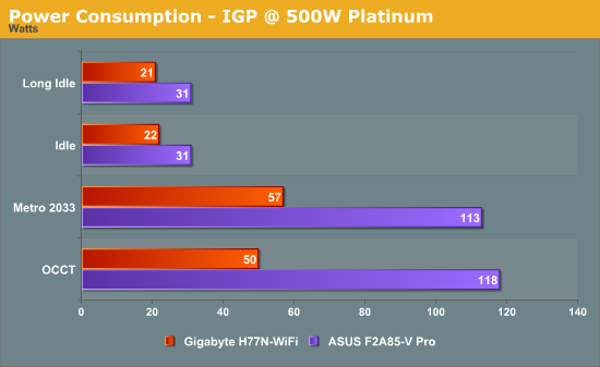
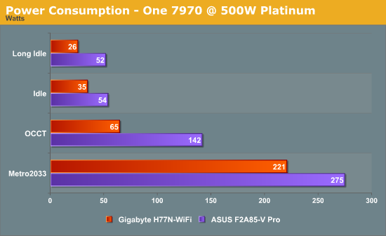
From our internal results, testing with 1 GPU on the 500W Platinum and 1250W Gold gave similar power readouts (Idle/OCCT/Metro on 500W gave 54/142/275, on 1250W gave 59/148/280), which means the 1250W is still good for comparison on the system. However for IGP testing, it was important to use the 500W. Our main comparison is the i3-3225 dual core Intel system on the to-be-reviewed Gigabyte H77N-WiFi, though the wattage between the processors accounts for large differences under load. At idle the larger ATX F2A85-V Pro does consume more power – if we get an ITX FM2 system, this will be a better comparison to test.
POST Time
Different motherboards have different POST sequences before an operating system is initialized. A lot of this is dependent on the board itself, and POST boot time is determined by the controllers on board (and the sequence of how those extras are organized). As part of our testing, we are now going to look at the POST Boot Time - this is the time from pressing the ON button on the computer to when Windows starts loading. (We discount Windows loading as it is highly variable given Windows specific features.) These results are subject to human error, so please allow +/- 1 second in these results.
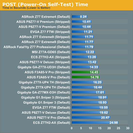
The F2A85-V Pro uses ASUS’ new CAP BIOS system, designed to aid in POST times across their motherboard range. It helps a little here, as normally for ATX boards POST times are in the 16+ second region – the CAP BIOS reduces this to just under 15 seconds.
USB Speed
For this benchmark, we run CrystalDiskMark to determine the ideal sequential read and write speeds for the USB port using our 240 GB OCZ Vertex3 SSD with a SATA 6 Gbps to USB 3.0 converter. Then we transfer a set size of files from the SSD to the USB drive using DiskBench, which monitors the time taken to transfer. The files transferred are a 1.52 GB set of 2867 files across 320 folders – 95% of these files are small typical website files, and the rest (90% of the size) are the videos used in the Sorenson Squeeze test.
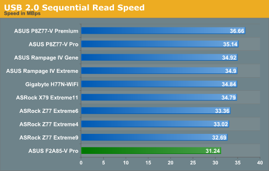
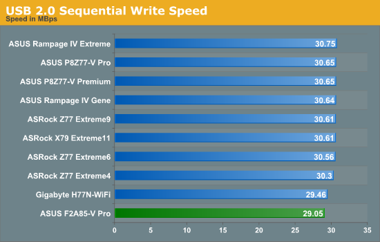
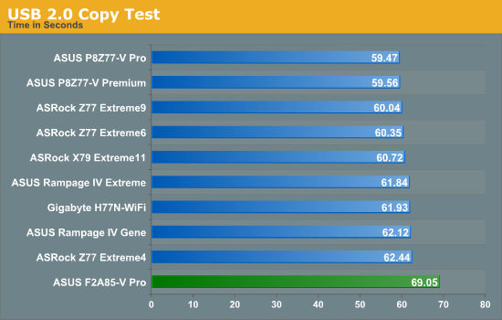
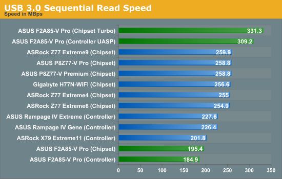
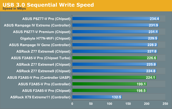
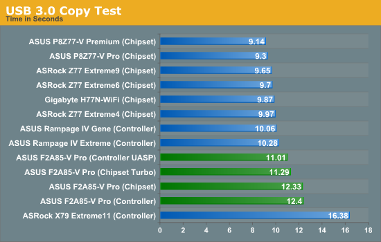
For whatever reason, our standard USB testing regimen on AMD systems shows a slight speed deficiency compared to the Intel systems. In USB 3.0 our copy tests are more than 10% slower on an AMD system.
SATA Testing
We also use CrystalDiskMark for SATA port testing on a C300 drive. The sequential test (incompressible data) is run at the 5 x 1000 MB level. This test probes the efficiency of the data delivery system between the chipset and the drive, or in the case of additional SATA ports provided by a third party controller, the efficiency between the controller, the chipset and the drive.
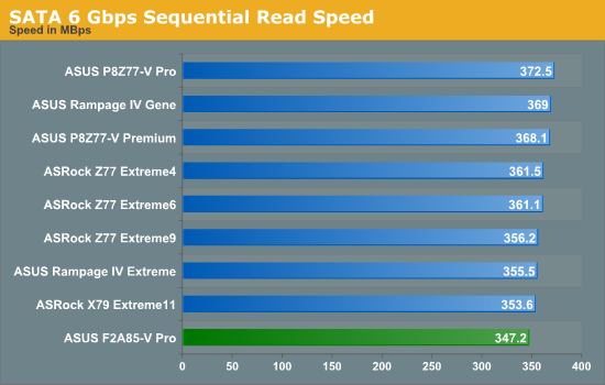
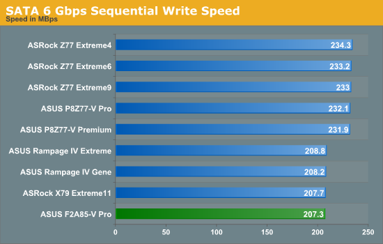
I really like the fact that the AMD chipset is SATA 6 Gbps only, although we see that SATA peak write speeds on this board are slightly lower than that of most Intel boards. Previously this is normally attributed to BIOS settings at default.
DPC Latency
Deferred Procedure Call latency is a way in which Windows handles interrupt servicing. In order to wait for a processor to acknowledge the request, the system will queue all interrupt requests by priority. Critical interrupts will be handled as soon as possible, whereas lesser priority requests, such as audio, will be further down the line. So if the audio device requires data, it will have to wait until the request is processed before the buffer is filled. If the device drivers of higher priority components in a system are poorly implemented, this can cause delays in request scheduling and process time, resulting in an empty audio buffer – this leads to characteristic audible pauses, pops and clicks. Having a bigger buffer and correctly implemented system drivers obviously helps in this regard. The DPC latency checker measures how much time is processing DPCs from driver invocation – the lower the value will result in better audio transfer at smaller buffer sizes. Results are measured in microseconds and taken as the peak latency while cycling through a series of short HD videos - under 500 microseconds usually gets the green light, but the lower the better.
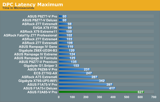
Normally our DPC Latency tests can be affected by monitoring software, producing a value north of 1000 microseconds. Anything under 500 is acceptable, and under 200 is great. However the F2A85-V Pro gets a value in the 600s. During the test, the DPC would hover between 100 and 200 most of the time, but every now and again would peak in the 600 region for whatever reason. The system was rebooted a couple of times but this behavior was persistent across boots. As of the 5104 BIOS this would be slightly worrying for audio work.
3D Movement Algorithm Test
The algorithms in 3DPM employ both uniform random number generation or normal distribution random number generation, and vary in various amounts of trigonometric operations, conditional statements, generation and rejection, fused operations, etc. The benchmark runs through six algorithms for a specified number of particles and steps, and calculates the speed of each algorithm, then sums them all for a final score. This is an example of a real world situation that a computational scientist may find themselves in, rather than a pure synthetic benchmark. The benchmark is also parallel between particles simulated, and we test the single thread performance as well as the multi-threaded performance.
It should be noted that this benchmark is a purely floating point benchmark, indicative of a lot of research written code where several months of optimization is not possible or not common knowledge within the research group. The compiler is not clever enough to convert what is expected into appropriate integer conversions, so Bulldozer and Piledriver based processors will only perform as well as their singular FPU units per module will allow. The benchmark is unaffected by memory speed as thread creation is created on the CPU and all data created fits well within the L2 cache per core.
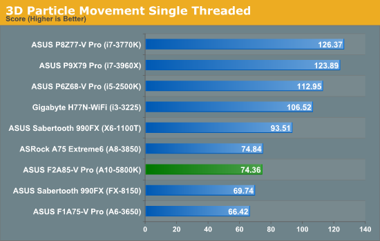
In the single threaded test, a lot of conclusions can be drawn from the comparison of AMD architectures. Direct comparison of Piledriver to Bulldozer (A10-5800K to FX-8150) gives a boost in single core performance of 7%, however comparing the old Stars cores of the A8-3850 at 2.9 GHz is roughly the same as the new Piledriver core at 4.2 GHz. So even with a 1.3 GHz advantage, Piledriver is only as good as Stars and less efficient in floating point results. If we compare Piledriver to Thuban, i.e. A10-5800K to X6 1100T, the Piledriver core gets stomped on by a good 25% performance. I find this quite staggering – most of the code I ever encountered as a computational chemist was floating point based, dealing with single and double precision on a regular basis. On this result, I would steer clear of Piledriver.
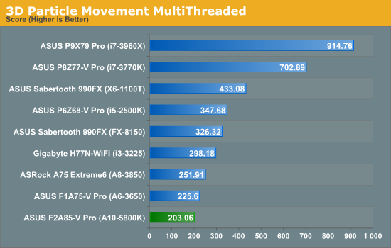
The multithreaded version of 3DPM is slightly tougher to analyze. Due to the FP nature of the program, the A10-5800K is essentially a 2 core FPU processor, whereas all the other comparative AMD processors have either 4 or 6 FPUs to play with. What is perhaps worth considering is that the Bulldozer processor with 4 modules scores 326.32, whereas the Piledriver processor with only 2 modules scores 203.06, which is more than half. This would mean that the Piledriver core actually achieves 20% better performance at the same frequency, despite our ST test giving Piledriver only a 7% increase. Part of this could be put down to the architecture improvements – improved scheduling for heavily threaded loads, one of the downfalls of Bulldozer but was improved in Piledriver could be the reason here.
WinRAR x64 3.93 - link
With 64-bit WinRAR, we compress the set of files used in the USB speed tests. WinRAR x64 3.93 attempts to use multithreading when possible, and provides as a good test for when a system has variable threaded load. If a system has multiple speeds to invoke at different loading, the switching between those speeds will determine how well the system will do. WinRAR is also very sensitive to memory speeds and subtimings.
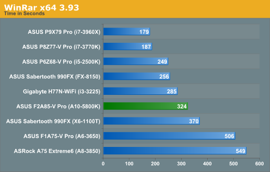
Analyzing the WinRAR results can be a little confusing, given that at different points of our previous testing the memory settings have been different (should point out that they have been consistent when comparing against like-for-like). When the A10-5800K was playing ball with DDR3-2400 10-12-12 memory, the WinRAR copy test pulled out miles ahead of the Thuban and Llano processors by a good margin. However the Sandy Bridge i5-2500K, with 4 INT and 4 FPU units gave the Trinity processor a proverbial thrashing despite being limited to DDR3-1333 at the time of testing.
FastStone Image Viewer 4.2 - link
FastStone Image Viewer is a free piece of software I have been using for quite a few years now. It allows quick viewing of flat images, as well as resizing, changing color depth, adding simple text or simple filters. It also has a bulk image conversion tool, which we use here. The software currently operates only in single-thread mode, which should change in later versions of the software. For this test, we convert a series of 170 files, of various resolutions, dimensions and types (of a total size of 163MB), all to the .gif format of 640x480 dimensions.
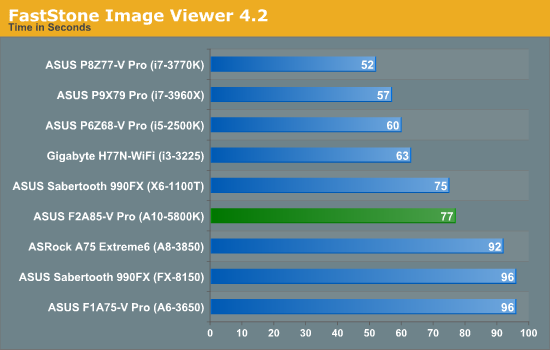
In the FastStone results, we see the Piledriver processor beat the Bulldozer and Stars cores by a considerable margin, and nudge the Thuban as well.
Xilisoft Video Converter
With XVC, users can convert any type of normal video to any compatible format for smartphones, tablets and other devices. By default, it uses all available threads on the system, and in the presence of appropriate graphics cards, can utilize CUDA for NVIDIA GPUs as well as AMD APP for AMD GPUs. For this test, we use a set of 32 HD videos, each lasting 30 seconds, and convert them from 1080p to an iPod H.264 video format using just the CPU. The time taken to convert these videos gives us our result.
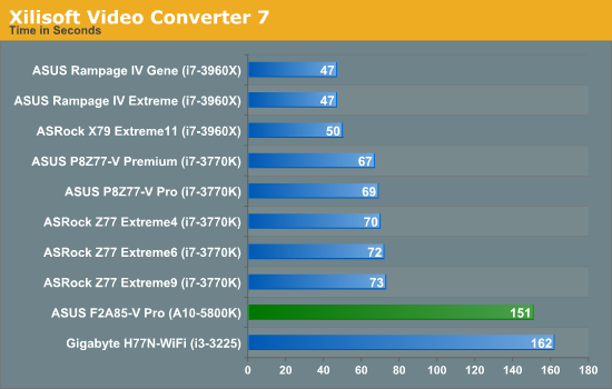
Unfortunately our Xilisoft benchmark is rather new, and thus we do not have results for all the AMD cores we have used in the past. However if we compare the A10-5800K directly with the i3-3225, we unfortunately have a memory difference to contend with (DDR3-2133 vs. DDR3-1600). With that being said, it is clear that video conversion is an INT process and all four of the A10-5800K INT units are being used.
x264 HD 4.0.1 Benchmark
The x264 HD Benchmark uses a common HD encoding tool to process an HD MPEG2 source at 1280x720 at 3963 Kbps. This test represents a standardized result which can be compared across other reviews, and is dependant on both CPU power and memory speed. The benchmark performs a 2-pass encode, and the results shown are the average of each pass performed four times.
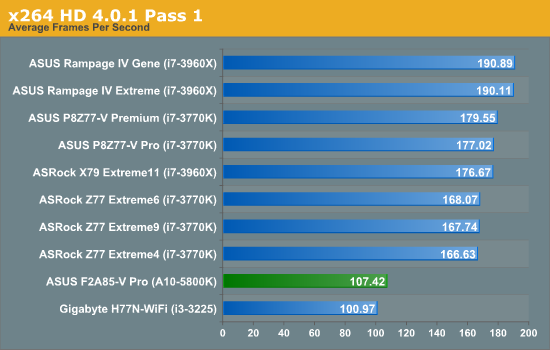
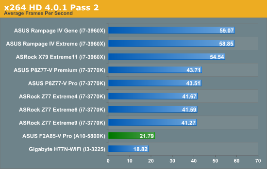
As part of the ever evolving motherboard benchmark suite, it has been suggested that we add in a few new benchmarks. In this case, we have added Portal 2 using the same timedemo from our GPU and Notebook reviews, and Batman: Arkham Asylum using the in game benchmark.
Portal 2
A stalwart of the Source engine, Portal 2 is the big hit of 2011 following on from the original award-winning Portal. In our testing suite, Portal 2 performance should be indicative of CS:GO performance to a certain extent. Here we test Portal 2 at 2560x1440 with maximum graphical setting using the same timedemo used in our GPU and notebook reviews.
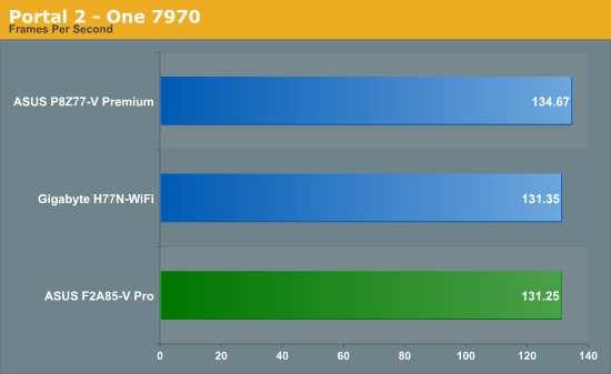
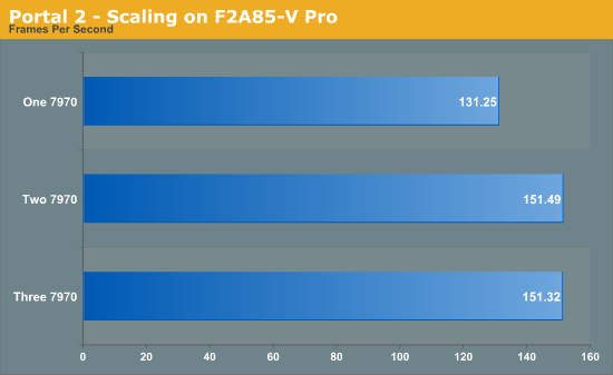
Portal 2 seems to enjoy the GPU power, and CPU power does not matter as much. Scaling beyond 2 AMD GPUs on Trinity seems non-existant.
Dirt 3
Dirt 3 is a rallying video game and the third in the Dirt series of the Colin McRae Rally series, developed and published by Codemasters. Using the in game benchmark, Dirt 3 is run at 2560x1440 with full graphical settings. Results are reported as the average frame rate across four runs.
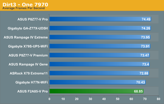
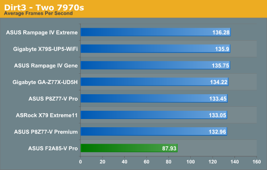
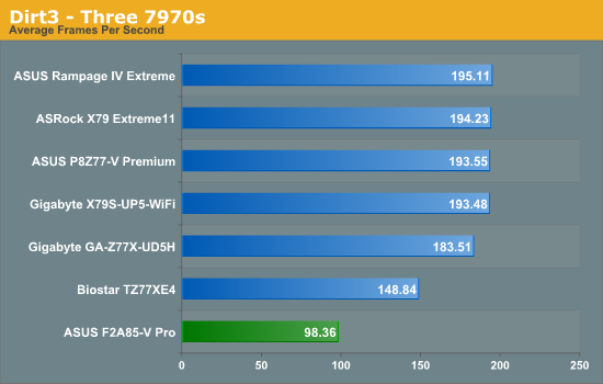
As seen in the past, Dirt3 on AMD loves CPU MHz, GPU horsepower, everything. In the case of Trinity, the lack of grunt by the CPU does give it a lower result than the rest of our testing. Three-way GPU is crippled by that 4x PCIe 2.0 port at the bottom of the board.
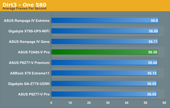
In contrast, using an NVIDIA GPU means that the GPU becomes the limiting factor rather than the CPU.
Metro2033
Metro2033 is a DX11 benchmark that challenges every system that tries to run it at any high-end settings. Developed by 4A Games and released in March 2010, we use the inbuilt DirectX 11 Frontline benchmark to test the hardware at 2560x1440 with full graphical settings. Results are given as the average frame rate from 4 runs.
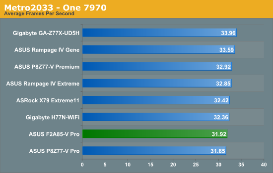
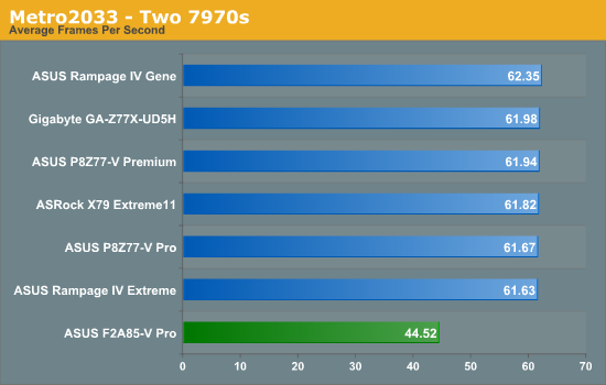
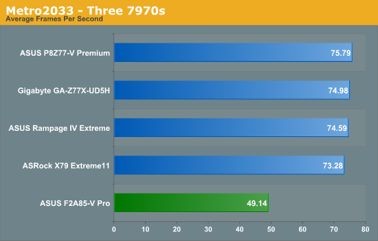
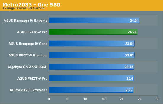
With Metro2033 we see similar results to Dirt3 - on AMD scaling is not that great and the GPU needs some CPU power to keep being fed. On AMD the results are better, making the GPU the limiting factor.
Batman Arkham Asylum
Made in 2009, Batman:AA uses the Unreal Engine 3 to create what was called “the Most Critically Acclaimed Superhero Game Ever”, awarded in the Guinness World Record books with an average score of 91.67 from reviewers. The game boasts several awards including a BAFTA. Here we use the in-game benchmark while at the highest specification settings without PhysX at 2560x1440. Results are reported to the nearest FPS, and as such we take 4 runs and take the average value of the final three, as the first result is sometimes +33% more than normal.
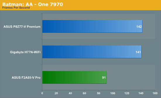
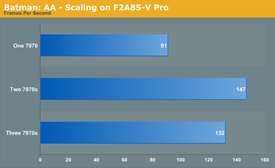
Our Batman results are highly odd. On one card it seems that the CPU holds the frame rate back, but in a three-way GPU setup the frame rate decreases - this may due to the 4x PCIe 2.0 port is restricting data flow needed by other GPUs.
Final Words
Concluding a review of the first motherboard of a new chipset is difficult. New chipset usually means new processors, so a lot of what a reviewer has to say ends up being more about the processors in question. As a performance enthusiast that means I am not that happy with Trinity as a performance product – the Piledriver cores leave a lot to be desired. The processor trades a lot of blows with the i3-3225 results we included in the testing, but the big ‘stick out like a sore thumb’ point of contention for me was the single thread performance in 3DPM – 106.52 scored by the i3-3225 at 3.3 GHz against 74.36 scored by the A10-5800K at 4.2 GHz. This obviously has a knock on effect in gaming, whereby a lot of modern games still require a decent single core speed to deliver the best performance, and AMD knew this so the increase in the IGP was expected. As mentioned in Anand’s Trinity article, as a result the Trinity IGP outperforms the HD4000 by a good margin, making small screen gaming enjoyable.
But this is a motherboard review, the first of the new chipset. The F2A85-V Pro retails for $140, more than the high end Trinity processor. That is a tough pill to swallow on any platform, regardless of processor, so there has to be functionality to match. The main message ASUS likes to give is the wealth of experience and R&D that underpin every product – additional controllers on board that help with power management, control over the power delivery, control over the fans and control over the network ports. ASUS boards are easy to use, and for a large part deliver what a user should want or need in the experience of a motherboard product.
With FM2 giving eight SATA 6 Gbps ports, there is no real reason to add extra SATA controllers, so none are added here. We get an extra ASMedia USB 3.0 controller though to take the USB 3.0 ports to six in total – the ASMedia controller can take advantage of the UASP protocol through ASUS’ software. We have the full gamut of video outputs, and I was surprised to learn that the DVI-D output took like a duck to water when plugged in to my Korean 27” – flawless in applying BIOS and OS visuals to which Ivy Bridge does not.
Performance wise there was only one obvious point of concern - the DPC Latency which spiked to 600 microseconds under normal usage. This should be fixed with a BIOS update.
Overclocking seemed like a never ending process, but we ended up with 4.5 GHz on our review sample. Again there is not much we can draw from this result, except the fact that 300 MHz is not a large overclock on a chip that has a turbo mode of 4.2 GHz. This is shown clearly by ASUS’ auto overclocking software, which only achieves 4.3 GHz and 4.4 GHz on ‘Fast’ and ‘Extreme’ settings respectively.
As much as Trinity is cementing the base for AMD’s future growth in terms of architecture, Ivy Bridge has such a lead on the CPU space that there are few reasons to jump on board to Trinity. As part of an IGP based system, such as a HTPC, there are many merits to Trinity as Ganesh has found out. From my perspective, a storage system the RAID 5 that the A85X chipset supports across the eight SATA 6 Gbps ports is golden where Trinity is concerned.
Addendum 10/17: When this review was first published, I showed some incorrect results from monitoring voltages. Unfortunately I attributed this to the potential behavior of the motherboard, but further tests have indicated that the third-party software was at fault. We have pulled the results to remove confusion and would like to apologize to ASUS for this error.

