Original Link: https://www.anandtech.com/show/6337/samsung-ssd-840-250gb-review
Samsung SSD 840 (250GB) Review
by Kristian Vättö on October 8, 2012 12:14 PM EST- Posted in
- Storage
- SSDs
- Samsung
- TLC
- Samsung SSD 840
Introduction
Samsung has been making steady progress in becoming one of the major players in the consumer SSD market. Even before the SSD 470, Samsung was a major player in the industry with their mostly OEM SSDs, but this took a dramatic change when the SSD 830 was released. Samsung never really marketed the SSD 470, even though it was a reasonable competitor back at its launch. The SSD 830 was Samsung’s first SSD that really received media and consumer attention, and for good reason: it was one of the best consumer SSDs on the market.
With the 840 and 840 Pro, Samsung took a big step forward in marketing. Instead of hosting a regular press release and providing reviewers with the drives, Samsung flew around 70 media representatives from all around the world to Seoul, South Korea for their Global SSD Summit. Samsung spent two days talking about their new drives, including several live demos and presentations on Samsung’s future plans. For the first time, Samsung also opened the doors of one their NAND manufacturing plants to media and we were allowed to meet with some of their engineers in person and ask questions about their NAND and SSDs.
We have already reviewed the 840 Pro, but Samsung did not sample the regular 840 until the Summit. I started testing the 840 right after I got back from Seoul and I was able to provide you with some preliminary benchmarks shortly after, but today we’re back with the full review.
When we finally got the specifications for the SSD 840, I understood why Samsung was reluctant to share too many details about the drive before its launch: the Samsung SSD 840 is the first consumer SSD to utilize 3-bit-per-cell MLC NAND (aka TLC). Before we delve into the actual SSD 840, let's take a closer look at how NAND works and how TLC compares to SLC and MLC.
A TLC Refresher
Back in February, we published an article called Understanding TLC NAND, where we went in-depth about how NAND works and the differences between various kinds of NAND (SLC, MLC, and TLC). Back then we didn't know when TLC SSDs would be publicly available or who would be the first manufacturer. Supposedly, OCZ had interest in releasing TLC based SSDs but the supply of TLC NAND wasn't good enough for their needs. Samsung has the benefit of being a tier one manufacturer that makes its own NAND, which gives it an advantage when dealing with new technologies as it can control the output of NAND. In this case, Samsung was able to ramp up the production of TLC NAND when it wanted to, whereas OCZ must live with whatever the NAND manufacturers are ready to sell them.
While we have covered TLC in detail already, we have some new details to add:
| SLC | MLC | TLC | |
| Bits per Cell | 1 | 2 | 3 |
| P/E Cycles | 100,000 | 3,000 | 1,000 |
| Read Time | 25us | 50us | ~75us |
| Program Time | 200-300us | 600-900us | ~900-1350us |
| Erase Time | 1.5-2ms | 3ms | ~4.5ms |
Samsung would not tell us the exact read, program, and erase latencies but they told us that their TLC is around 50% slower than their MLC NAND. We don't know the latencies for Samsung's MLC NAND either, hence we have to go by general MLC NAND latencies, which varies a lot depending on process. However, we were able to get the P/E cycle count for TLC, which is 1,000. Samsung did not specify the process node but given that they listed MLC at 3,000 cycles, we are most likely talking about 27nm or 21nm. I wouldn't find it unlikely that Samsung is rating their 21nm MLC NAND at 3,000 P/E cycles as well because IMFT was able to keep the endurance at the same level with their 20nm MLC NAND.
Physically, TLC is similar to SLC and MLC. All three consist of similar transistors, the only difference is that they store a different amount of bits per cell. SLC only stores one, whereas MLC stores two and TLC stores three. This actually creates a minor problem, as there is no multiple of three that is a power of two. Unlike with hard drives, SSD capacities typically go in powers of two, such as 64GB, 128GB, and 256GB.
NAND is actually built based on binary prefixes (Mebi, Gibi...) but is almost always referred to using metric prefixes (Mega, Giga...). For example a 128GB SSD has ~137.4GB of storage (128GiB) due to Gibi to Giga translation, but the remaining space is used as spare area.
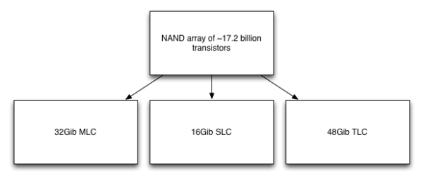
If the raw NAND array has 17.2 billion transistors, you would get 16Gibibits (17.2Gbits) of storage with SLC NAND because each cell can store one bit of data. MLC yields 32Gib, which is still a nice power of two because all you're doing is adding one level. However, with TLC you get 48Gib, which is not a power of two. Technically nothing is stopping manufacturers from making a 48Gib die, but from the marketing and engineering standpoint it's much easier to stick with powers of two. A TLC die in this case should be 32Gib just like MLC. To achieve that, the die is simply reduced in size to around 11.5 billion transistors. 32Gib isn't exactly divisible by three, but thanks to spare bits it doesn't have to be. The trick here is that the same capacity TLC die is smaller than an MLC die, which results in more dies per wafer and hence lower production costs.
Lower Endurance—Why?
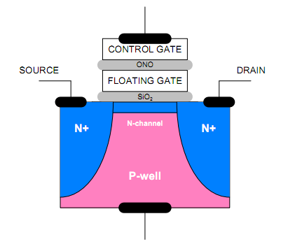
Below we have a diagram of a MOSFET (Metal Oxide Semiconductor Field Effect Transistor). When programming a cell, voltage is placed on the control gate, which forms an electric field that allows electrons to tunnel through the silicon oxide barrier to the floating gate. Once the tunneling process is complete, voltage to the control gate is dropped back to 0V and the silicon oxide acts as an insulator. Erasing a cell is done in a similar way but this time the voltage is placed on the silicon substrate (P-well in the picture), which again creates an electric field that allows the electrons to tunnel through the silicon oxide.
While the MOSFET is exactly the same for SLC, MLC and TLC, the difference lies in how the cell is programmed. With SLC, the cell is either programmed or it's not because it can only be "0" or "1". As MLC stores two bits in one cell, its value can either be "00", "01", "10" or "11", which means there are four different voltage states. TLC ups the voltage states to eight as there are eight different combinations of "0" and "1" when grouped in groups of three bits. Below are diagrams showing the graphical version of the voltage states:
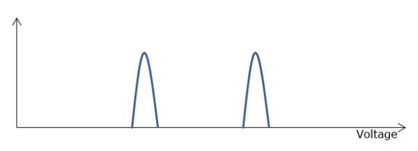
SLC
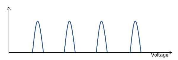
MLC
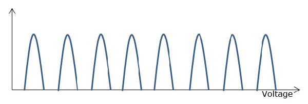
TLC
The above diagrams show the voltages for brand new NAND—everything looks nice and neat and the only difference is that TLC has more states. However, the tunneling process that happens every time the cell is programmed or erased wears the silicon oxide out. The actual oxide is only about 10nm thick and it gets thinner every time a smaller process node is introduced, which is why endurance gets worse as we move to smaller nodes. When the silicon dioxide wears out, atomic bonds break and some electrons may get trapped inside the oxide during the tunneling process. That builds up negative charge in the silicon oxide, which in turn negates some of the control gate voltage when the cell is programmed.
The wear results in longer erase times because higher voltages need to be applied for longer times before the right voltage is found. Remember, the controller can't adjust to changes in program and erase voltages (well, some can; more on this on the next page) that come from the trapped electrons, cell leakage, and other sources. If the voltage that's supposed to work doesn't, the controller has to basically go on guess basis and simply try different voltages before the right one is found. That takes time and causes even more stress on the silicon oxide.
The difference between SLC, MLC, and TLC is pretty simple: SLC has the fewest voltage states and hence it can tolerate bigger changes in voltages. With TLC, there are eight different states and hence a lot less voltage room to play with. While the exact voltages used are unknown, you basically have to divide the same voltage into eight sections instead of four or two like the graphs above show, which means the voltages don't have room to change as much. The reason why a NAND block has to be retired is that erasing it starts to take too long, which impacts performance (and eventually a NAND block simply becomes nonfunctional, e.g. the voltage states for 010 and 011 begin to overlap).
There is also more and more ECC needed as the NAND wears out because the possibility for errors is greater. With TLC, that's once again a bigger problem because there are three bits to correct instead of one or two. While today's ECC engines are fairly powerful, at some point it will be easier to just retire the block than to keep correcting errors.
Lower Endurance: Hardly an Issue
With perfect wear-leveling and write amplification of 1x, you would get 256,000GiB (that's ~275TB) of writes out of a 250GB Samsung 840 with TLC NAND and 1,000 P/E cycles. That is still a lot but wear-leveling and write amplification are never perfect. Giving any specific numbers for endurance is hard because every drive behaves differently and users have different workloads, but it's unlikely for a light consumer workload to see more than 10GiB of writes per day. That's 3,650GiB per year, which is only 1.4% out of 256,000GiB. In the real world NAND writes will be bigger than host writes but even with a write amplification factor of 10x, you will only end up writing 36,500GiB each year and exhausting ~143 P/E cycles out of the available 1,000. In other words, it would take roughly seven years for you to wear out the NAND.
| SSD Lifetime Estimation | ||||
| NAND | MLC—3K P/E Cycles | TLC—1K P/E Cycles | ||
| NAND Capacity | 128GiB | 256GiB | 128GiB | 256GiB |
| Writes per Day | 10GiB | 10GiB | 10GiB | 10GiB |
| Write Amplification | 10x | 10x | 10x | 10x |
| Total Estimated Lifespan | 10.5 years | 21.0 years | 3.5 years | 7.0 years |
For the 120GB Samsung 840, the lifespan is half of the 250GB model but we are still talking about years. Samsung doesn't offer a 60/64GB Samsung 840, although that makes sense as it wouldn't be hard to wear that out in less than three years, which is the warranty Samsung gives to the 840 SSD.
DSP to the Rescue
However, there is actually more to SSD endurance than just P/E cycles and write amplification. There has been a lot of talk lately about digital signal processing (DSP) in the industry, which is supposedly the solution for lower endurance NAND.
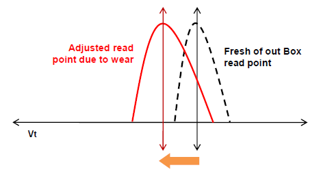
The basic idea behind DSP is very simple: you read changes in voltages and adapt to the changes. As I mentioned in the previous page, the voltages change as the NAND wears out and if your controller can't adapt to the changes, you'll be stressing the NAND even more. Each time you're trying to program or erase the cell, you are wearing it out, so you don't even have to succesfully program or erase the cell to cause damage. That's why the guess and test process for writing to NAND is so harmful; it may take multiple tries and each try will wear out the NAND even more.
Graphical presentation of a change in voltage state
However, if your controller can read the changes in program and erase voltages, you will know what voltages to use to program/erase the cell. Even though DSP doesn't make NAND immortal, it causes a lot less stress on the NAND, allowing it to last for more P/E cycles than what you would get without DSP.
Again, it's hard to give out any specific numbers of DSP usefulness in real world, but for example STEC is claiming that their CellCare technology can extend the endurance of regular 3K P/E cycle MLC up to as much as 60K. I've heard unofficial figures as high as 100K for some companies' DSPs, but I would take all figures with a grain of salt until they are tested by a third party. Either way, even if a good DSP is only able to double the endurance of NAND, it's a huge deal as we move to even smaller process nodes and possibly even more bits per cell.
The Samsung SSD 840
Now it's time to look at the Samsung SSD 840 itself. Performance differences between different capacities are tangible. Sequential write speed in particular increase with larger capacities. With MLC NAND based SSDs 256GB and 512GB models usually perform around the same because 256GB of NAND is able to saturate the limits of the controller but as TLC NAND has longer program times, you will need more NAND dies to hide the additional latency.
| Samsung SSD 840 Specifications | |||
| Capacity | 120GB | 250GB | 500GB |
| Sequential Read | 530MB/s | 540MB/s | 540MB/s |
| Sequential Write | 130MB/s | 250MB/s | 330MB/s |
| 4KB Random Read | 86K IOPS | 96K IOPS | 98K IOPS |
| 4KB Random Write | 32K IOPS | 62K IOPS | 70K IOPS |
| Cache (LPDDR2) | 256MB | 512MB | 512MB |
| Samsung SSD 840 Pro vs 840 vs 830 | ||||
| Samsung SSD 830 (256GB) | Samsung SSD 840 (250GB) | Samsung SSD 840 Pro (256GB) | ||
| Controller | Samsung MCX | Samsung MDX | Samsung MDX | |
| NAND | 27nm Toggle-Mode 1.1 MLC | 21nm Toggle-Mode 2.0 TLC | 21nm Toggle-Mode MLC | |
| Sequential Read | 520MB/s | 540MB/s | 540MB/s | |
| Sequential Write | 400MB/s | 250MB/s | 520MB/s | |
| Random Read | 80K IOPS | 96K IOPS | 100K IOPS | |
| Random Write | 36K IOPS | 62K IOPS | 90K IOPS | |
| Warranty | 3 years | 3 years | 5 years | |
Performance wise the 840 does well but can't challenge the 840 Pro. Read performance is actually nearly on-par with the 840 Pro but write performance is behind due to the use of TLC NAND. I should add that write speeds are still adequate for a consumer drive. In some ways, the 840 can still be a healthy upgrade from the 830. Even though sequential write speed is lower, the increase in random read and write speeds can compensate. Still I suspect most 830 users will want to upgrade to the 840 Pro at least, if they choose not to wait for the next generation of SSDs.
| Samsung SSD 840 Series Pricing | ||||||
| 64GB | 128GB | 256GB | 512GB | |||
| Samsung SSD 840 | N/A | $109.99 (120GB) | $199.99 (250GB) | $449.99 (500GB) | ||
| Samsung SSD 840 Pro | $99.99 | $149.99 | $269.99 | $599.99 | ||
Pricing isn't as aggressive as it could be but keep in mind that the above prices are suggested retail prices. Street prices can easily be ~$20 less and I wouldn't be surprised to see the 120GB SSD 840 retailing for less than $100 (and even $70-80 when on sale). Also note that we're still very early in the production of TLC NAND. Over time you can expect a more appreciable difference in pricing between TLC and MLC NAND.
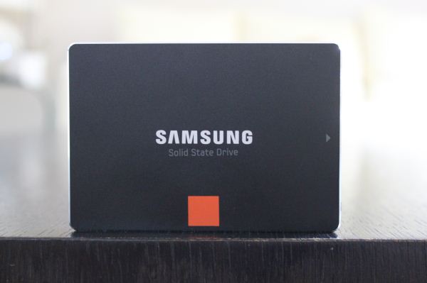
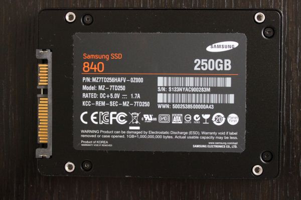
Based on the chassis alone you can't really tell the difference between the 840 and 840 Pro. Both use a similar matte black plastic design. The 840 measures in at 7mm tall as well, just like the 840 Pro. It's only when you flip the drive around that you can see that it's actually an 840 and not 840 Pro.
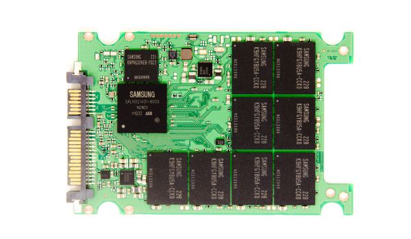
Unfortunately, we don't have any pictures of the internals at the moment. Samsung uses special pentalobe screws (similar to MacBook Air) and finding suitable screw drivers in Finland isn't as easy as in the US. In order to get the review out as soon as possible, we decided not to wait for the screwdriver to arrive from the US. We are, however, looking at a PCB that's indentical to the 840 Pro (i.e. eight 32GB TLC NAND packages). The only difference are NAND part numbers.
The 840 Pro
Test System
| CPU |
Intel Core i5-2500K running at 3.3GHz (Turbo and EIST enabled) |
| Motherboard |
AsRock Z68 Pro3 |
| Chipset |
Intel Z68 |
| Chipset Drivers |
Intel 9.1.1.1015 + Intel RST 10.2 |
| Memory | G.Skill RipjawsX DDR3-1600 2 x 4GB (9-9-9-24) |
| Video Card |
XFX AMD Radeon HD 6850 XXX (800MHz core clock; 4.2GHz GDDR5 effective) |
| Video Drivers | AMD Catalyst 10.1 |
| Desktop Resolution | 1920 x 1080 |
| OS | Windows 7 x64 |
Random Read/Write Speed
The four corners of SSD performance are as follows: random read, random write, sequential read and sequential write speed. Random accesses are generally small in size, while sequential accesses tend to be larger and thus we have the four Iometer tests we use in all of our reviews.
Our first test writes 4KB in a completely random pattern over an 8GB space of the drive to simulate the sort of random access that you'd see on an OS drive (even this is more stressful than a normal desktop user would see). I perform three concurrent IOs and run the test for 3 minutes. The results reported are in average MB/s over the entire time. We use both standard pseudo randomly generated data for each write as well as fully random data to show you both the maximum and minimum performance offered by SandForce based drives in these tests. The average performance of SF drives will likely be somewhere in between the two values for each drive you see in the graphs. For an understanding of why this matters, read our original SandForce article.
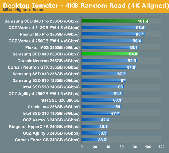
Random read speed is good but not 840 Pro level. Some of this can be due to the slower NAND as the queue depth of our random read test is only 3—with higher queue depths the difference between 840 and 840 Pro should be closer.
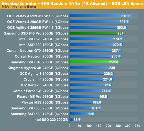
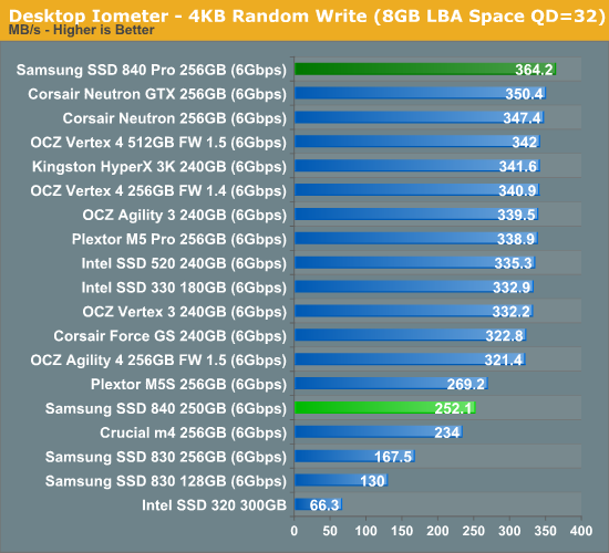
Random write speed is a bit odd as performance does not scale up with higher queue depths. Speculating on the cause is difficult, but if I had to guess I would say it's firmware related, not NAND this time. Samsung is most likely doing some very aggressive write combining and caching so it's easy to achieve the same level of performance regardless of queue depth.
Sequential Read/Write Speed
To measure sequential performance I ran a 1 minute long 128KB sequential test over the entire span of the drive at a queue depth of 1. The results reported are in average MB/s over the entire test length.
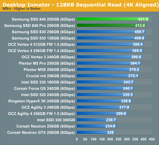
Samsung's read centric firmware approach with the 840 really shows off in our low queue depth sequential read test: there is no drive faster than it.
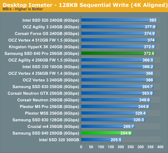
Sequential write is pretty poor compared to today's other 256GB SSDs but Samsung is only claiming 250MB/s so this shouldn't come as a surprise. The similarity between random and sequential write speed helps back up what we mentioned earlier: Samsung is likely being very aggressive with its write combining to make random IOs look very sequential.
AS-SSD Incompressible Sequential Performance
The AS-SSD sequential benchmark uses incompressible data for all of its transfers. The result is a pretty big reduction in sequential write speed on SandForce based controllers, while other drives continue to work at roughly the same speed as with compressible data.
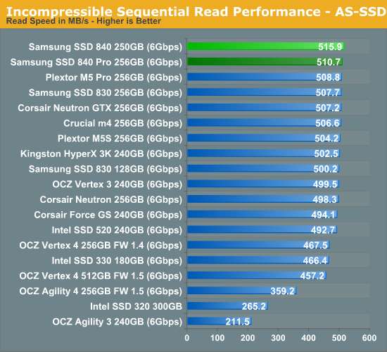
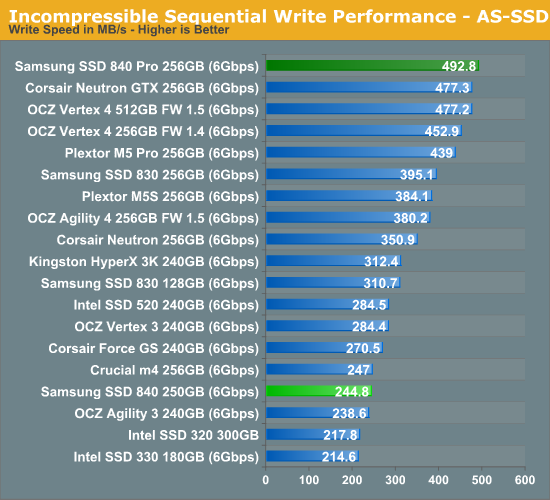
Incompressible sequential read/write speeds concur with our IOmeter tests: Read speed is great but write performance is distinctly previous gen.
Performance vs. Transfer Size
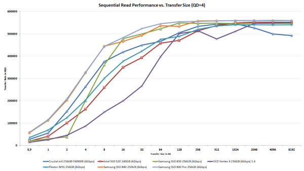
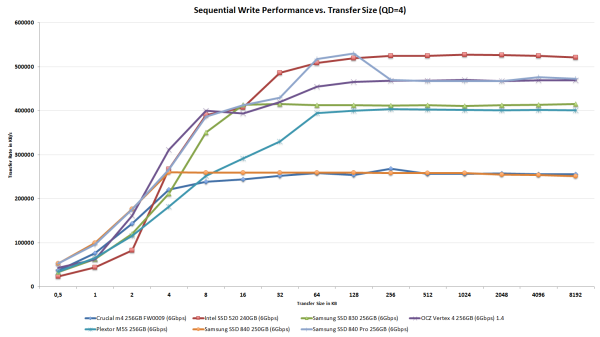
ATTO is a useful tool for quickly measuring the impact of transfer size on performance. Similarly to the 840 Pro, the 840 is a high performer at small transfer sizes, which is an area I think too many SSD vendors are ignoring. Not all IOs are huge in size and while the small IO read/write speeds aren't big enough to be used for marketing, they play a role in real world performance. In write speed the 840 tops out at 250MB/s, which is low compared to many other SSDs but otherwise the 840 performs very well.
Click for full size
AnandTech Storage Bench 2011
Last year we introduced our AnandTech Storage Bench, a suite of benchmarks that took traces of real OS/application usage and played them back in a repeatable manner. Anand assembled the traces out of frustration with the majority of what we have today in terms of SSD benchmarks.
Although the AnandTech Storage Bench tests did a good job of characterizing SSD performance, they weren't stressful enough. All of the tests performed less than 10GB of reads/writes and typically involved only 4GB of writes specifically. That's not even enough exceed the spare area on most SSDs. Most canned SSD benchmarks don't even come close to writing a single gigabyte of data, but that doesn't mean that simply writing 4GB is acceptable.
Originally we kept the benchmarks short enough that they wouldn't be a burden to run (~30 minutes) but long enough that they were representative of what a power user might do with their system. Later, however, we created what we refer to as the Mother of All SSD Benchmarks (MOASB). Rather than only writing 4GB of data to the drive, this benchmark writes 106.32GB. This represents the load you'd put on a drive after nearly two weeks of constant usage. And it takes a long time to run.
1) The MOASB, officially called AnandTech Storage Bench 2011—Heavy Workload, mainly focuses on the times when your I/O activity is the highest. There is a lot of downloading and application installing that happens during the course of this test. Our thinking was that it's during application installs, file copies, downloading, and multitasking with all of this that you can really notice performance differences between drives.
2) We tried to cover as many bases as possible with the software incorporated into this test. There's a lot of photo editing in Photoshop, HTML editing in Dreamweaver, web browsing, game playing/level loading (Starcraft II and WoW are both a part of the test), as well as general use stuff (application installing, virus scanning). We included a large amount of email downloading, document creation, and editing as well. To top it all off we even use Visual Studio 2008 to build Chromium during the test.
The test has 2,168,893 read operations and 1,783,447 write operations. The IO breakdown is as follows:
| AnandTech Storage Bench 2011—Heavy Workload IO Breakdown | ||||
| IO Size | % of Total | |||
| 4KB | 28% | |||
| 16KB | 10% | |||
| 32KB | 10% | |||
| 64KB | 4% | |||
Only 42% of all operations are sequential; the rest ranges from pseudo to fully random (with most falling in the pseudo-random category). Average queue depth is 4.625 IOs, with 59% of operations taking place in an IO queue of 1.
Many of you have asked for a better way to really characterize performance. Simply looking at IOPS doesn't really say much. As a result we're going to be presenting Storage Bench 2011 data in a slightly different way. We'll have performance represented as Average MB/s, with higher numbers being better. At the same time we'll be reporting how long the SSD was busy while running this test. These disk busy graphs will show you exactly how much time was shaved off by using a faster drive vs. a slower one during the course of this test. Finally, we will also break out performance into reads, writes, and combined. The reason we do this is to help balance out the fact that this test is unusually write intensive, which can often hide the benefits of a drive with good read performance.
There's also a new light workload for 2011. This is a far more reasonable, typical every day use case benchmark. It has lots of web browsing, photo editing (but with a greater focus on photo consumption), video playback, as well as some application installs and gaming. This test isn't nearly as write intensive as the MOASB but it's still multiple times more write intensive than what we were running last year.
We don't believe that these two benchmarks alone are enough to characterize the performance of a drive, but hopefully along with the rest of our tests they will help provide a better idea. The testbed for Storage Bench 2011 has changed as well. We're now using a Sandy Bridge platform with full 6Gbps support for these tests.
AnandTech Storage Bench 2011—Heavy Workload
We'll start out by looking at average data rate throughout our new heavy workload test:
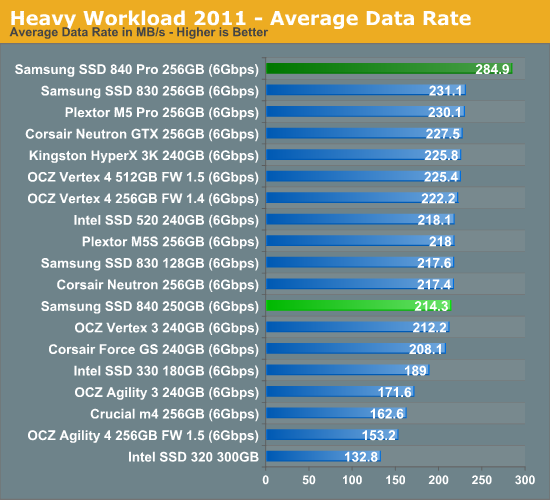
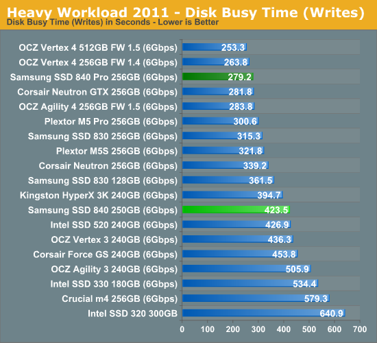
The 840 is quite average in our Heavy suite and performs similarly to most SandForce drives. The 840 Pro is a lot faster under heavy workloads, so it should be obvious by now why Samsung is offering two SSDs instead of one like they used to.
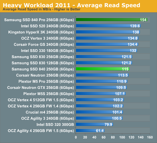
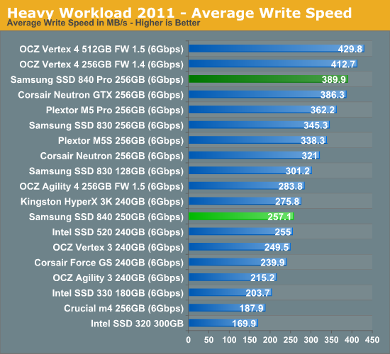
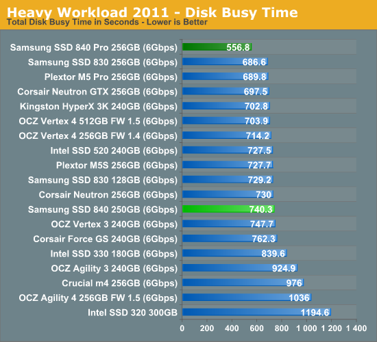
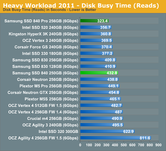
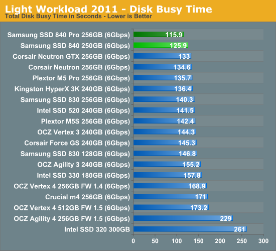
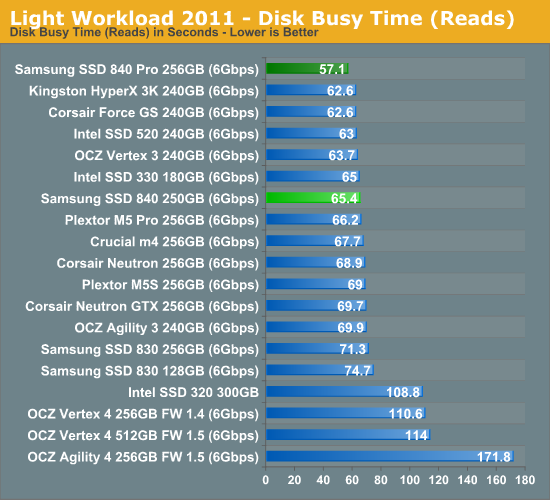
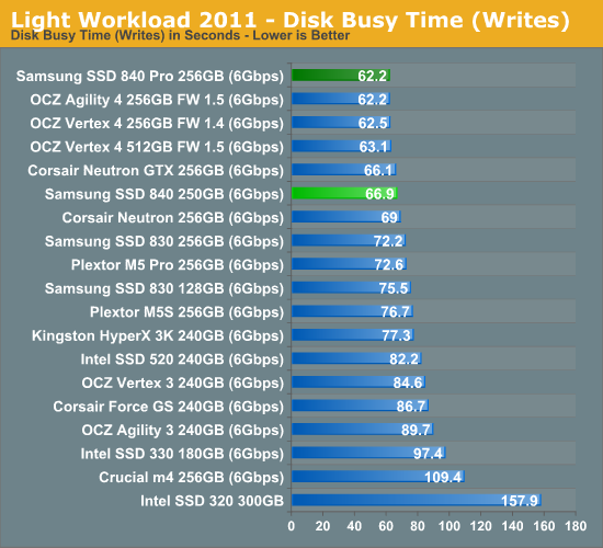
The next three charts just represent the same data, but in a different manner. Instead of looking at average data rate, we're looking at how long the disk was busy for during this entire test. Note that disk busy time excludes any and all idles, this is just how long the SSD was busy doing something:
AnandTech Storage Bench 2011—Light Workload
Our new light workload actually has more write operations than read operations. The split is as follows: 372,630 reads and 459,709 writes. The relatively close read/write ratio does better mimic a typical light workload (although even lighter workloads would be far more read centric).
The I/O breakdown is similar to the heavy workload at small IOs, however you'll notice that there are far fewer large IO transfers:
| AnandTech Storage Bench 2011—Light Workload IO Breakdown | ||||
| IO Size | % of Total | |||
| 4KB | 27% | |||
| 16KB | 8% | |||
| 32KB | 6% | |||
| 64KB | 5% | |||
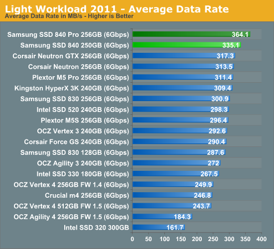
While the 840 didn't shine in our Heavy suite, it definitely takes the crown in our Light suite. The 840 Pro is still faster, obviously, but the 840 is the second fastest SSD we have tested. As the 840 is aimed towards consumers, the Light workload test should be a better indication of overall performance than our Heavy suite.
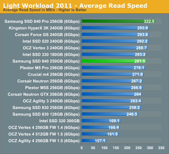
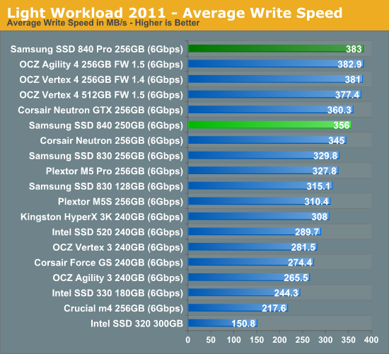
What's rather odd is that the average write speed is over 100MB/s higher than any synthetic write benchmark we ran.
Performance Over Time & TRIM
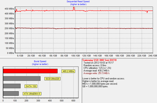
For starters, I ran HDtach on a secure erased drive to get the baseline performance:
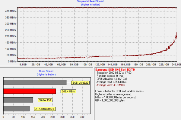
Next I secure erased the drive again, filled it with compressible data and proceeded with torturing it for 20 minutes with compressible 4KB random writes (100% LBA space, QD=32):
Ouch, performance takes a big hit. Usually 20 minutes isn't enough to put 256GB drives on their knees but it definitely is for the 840. Write speed drops to as low as 25MB/s, although it's nearly restored before all user-accessible LBAs have been filled. The way to avoid this worst case state is to keep as much free space on your drive as possible. We typically recommend around 20%, however with TLC NAND it might be advisable to bump that up to 30%. The 840 Pro will be a better option for heavy write workloads already due to its higher endurance.
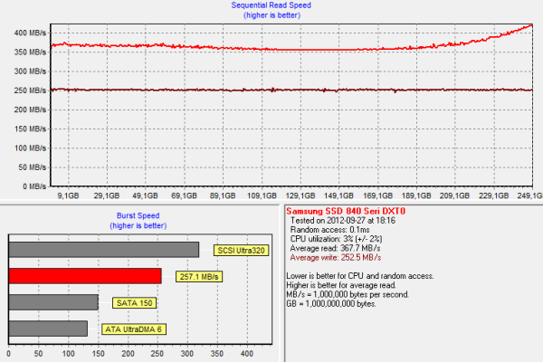
To see how idle time is able to restore performance, I let the drive idle for 50 minutes:
Write speed is fully restored but for some reason, read speed is fluctuating. The drop isn't huge as we are still talking about +350MB/s at all times, but it's interesting and a bit odd to see this kind of behavior since read speed was ~425MB/s after torture.
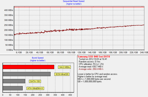
Finally I secure erased the drive again, filled it, tortured for 20 minutes and TRIM'ed it:
Again we see some weird behavior as write speed is not fully restored after TRIM. It does get to 250MB/s at the end of the HDtach run, but the starting performance is only 150MB/s. Keep in mind that I TRIM'ed the drive right after the torture; I didn't run HDtach in between like we often do but a functioning TRIM should still fully restore performance. Remember that TRIM is still just a suggestion—it's up to the controller to prioritize TRIMed LBAs for garbage collection. Given the higher program/erase latencies with TLC NAND it's entirely possible that the 840's garbage collection routine is just slower than we're used to seeing. Another possibility is that with the fewer number of P/E cycles, the 840 is just very conservative about using them when it's not stricly necessary (e.g. ignoring some of the TRIM "suggestions").
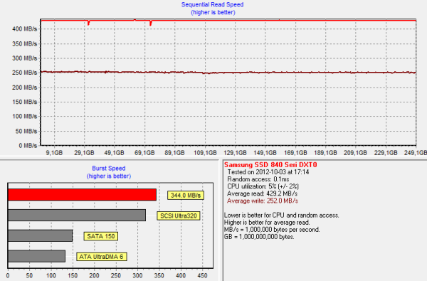
As a final test, I TRIM'ed the drive again and ran HDtach:
And now performance is what it should be. This is mostly due to sequential writes because at the end of the previous HDtach run, write performance was already at 250MB/s.
Power Consumption
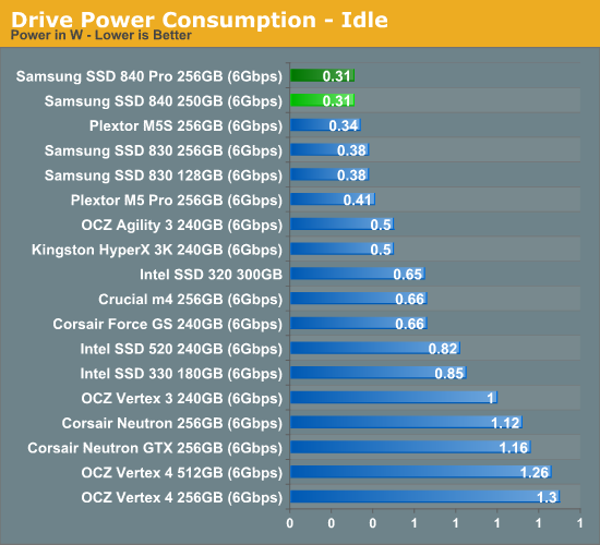
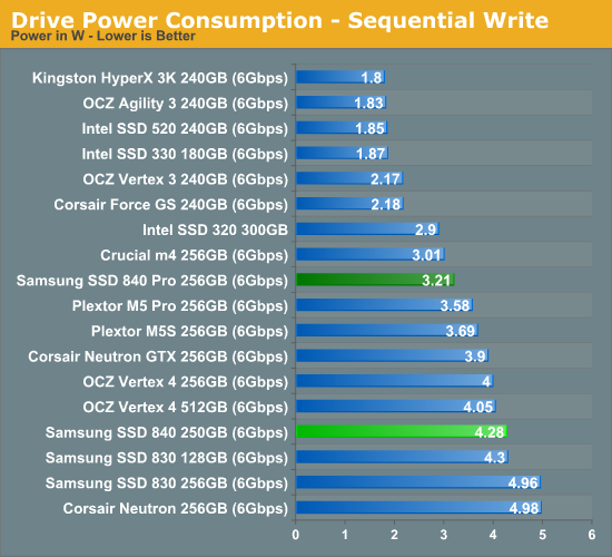
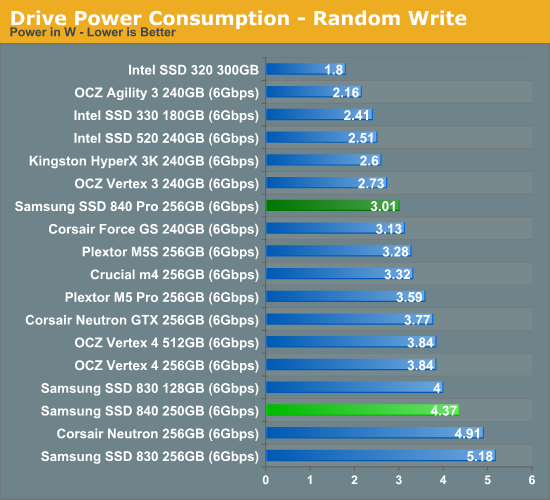
Idle power consumption is equal to the 840 Pro but active power consumption is noticeably higher. The 840 is supposed to have higher power consumption than the 840 Pro so this isn't a bug or flaw. Using NAND with more bits per cell requires a longer and more careful tunneling and it's possible that this is partially the reason for higher power consumption, though I believe it also has to do with the firmware and product differentiation (Samsung is fairly proud of the 840 Pro's power consumption).
Final Words
I have to say I was very skeptical when I first heard that the 840 will use TLC NAND. Samsung kept the TLC/MLC divide between the 840 and 840 Pro quiet until it took the stage at the SSD Summit for good reason. Prior to the 840's launch TLC NAND was mostly used in low cost devices (USB sticks, cheap tablets, etc...)—no one would dare throw a TLC drive into a high performance PC. However, after spending a week with the 840 running various tests, I'm pleasantly surprised. After seeing how slow NAND can impact performance with other drives I didn't have high hopes for the 840 when I heard it used TLC NAND.
Fortunately, the 840 exceeded all our expectations. It's faster, overall, than most of the previous generation MLC NAND based SSDs we have tested, which says a lot about Samsung's skill with it comes to designing a controller and firmware. When you take slower and lower endurance NAND, there is much more you have to do at the controller and firmware level to get things right. You can't sacrifice too much endurance for performance or vice versa. While long term endurance is still unproven, Samsung is definitely upping the ante in terms of low-cost SSD performance.
What's just as surprising is that Samsung is the first manufacturer with a TLC NAND based SSD. Samsung was under no pressure to release a TLC drive but it managed to beat the competition without sacrificing performance. Samsung hasn't been too aggressive in the past, but since the 830 it's clear the company has tapped some new found energy.
The 840 is very important for two reasons. For starters, it really shows the benefits of being a vertically integrated SSD maker. Samsung could easily coordinate SSD development with TLC NAND production ramps to make the 840 launch a seamless reality. The second aspect of the 840 that makes it so important is that this now gives the market a new solution to driving SSD prices down.
Prior to the 840, if you wanted a low cost SSD you either had to sacrifice on capacity or performance (or both). Sacrifice enough on capacity and you end up being forced into a SSD + HDD caching solution. Sacrifice enough on performance and you end up with a bad SSD. If TLC NAND pricing ramps to where it should be, the 840 can deliver the best of both worlds: low-cost pricing with all of the quality (and a lot of the performance) of a more expensive drive.
I'm less concerned about the 840's impact on other high end drive/controller makers and more interested to see what it does to companies like Phison or SanDisk. If Samsung can make its pricing aggressive enough, there should be no reason to consider any of the slower controllers for lower cost drives. We've been wondering about what it would take to get SSDs into truly mainstream PCs and it seems like the Samsung SSD 840 is exactly the right path to take.
In the end, a lot will be up to the final pricing but I believe Samsung can and will be very aggressive with the 840. Samsung is the only manufacturer with a price benefit thanks to the cheaper NAND, which at least in theory allows them to price themselves lower than anyone else. I'm sure we will see some MLC drives being sold for less than the 840, but it's very hard to challenge the 840 in terms of performance, especially when taking Samsung's reliability track record into account. Consider also that as recently as July 2012, Samsung's 830 was priced roughly 50% higher than the current street prices; with the 256GB 830 now going for $200 (and sometimes less with sales), that's likely where the 840 will start before continuing the downward trend.
We will see about final pricing in a couple of weeks, but for now the 840 looks like the entry level SSD to buy. The 840 Pro is likely the drive to buy for your primary notebook/workstation, while the 840 is the drive to recommend for a relative who isn't as concerned with performance and has a much lighter workload. I have to say, this is the first performance/value split of an SSD line that's really made sense.

