Original Link: https://www.anandtech.com/show/5911/nvidia-announces-retail-gt-640-ddr3
NVIDIA Announces Retail GeForce GT 640 DDR3
by Ryan Smith on June 4, 2012 9:00 PM ESTThough NVIDIA primarily likes to announce products on their own schedule and own time they have also been known to announce more budget oriented parts at trade shows, and with Computex Taiwan in full swing this week that’s exactly what’s happening. After some speculation and gnashing of the teeth by HTPC enthusiasts, NVIDIA is finally announcing their first retail GK107 part, the GeForce GT 640.
| GTS 450 | GT 640 DDR3 | GT 630 GDDR5 | GT 630 DDR3 | |
| Previous Model Number | N/A | New | GT 440 GDDR5 | GT 440 DDR3 |
| Stream Processors | 192 | 384 | 96 | 96 |
| Texture Units | 32 | 32 | 16 | 16 |
| ROPs | 16 | 16 | 4 | 4 |
| Core Clock | 783MHz | 900Mhz | 810MHz | 810MHz |
| Shader Clock | 1566MHz | N/A | 1620MHz | 1620MHz |
| Memory Clock | 3.6GHz GDDR5 | 1.782GHz DDR3 | 3.2GHz GDDR5 | 1.8GHz DDR3 |
| Memory Bus Width | 128-bit | 128-bit | 128-bit | 128-bit |
| Frame Buffer | 1GB | 2GB | 1GB | 1GB |
| GPU | GF106 | GK107 | GF108 | GF108 |
| TDP | 106W | 65W | 65W | 65W |
| Transistor Count | 1.17B | 1.3B | 585M | 585M |
| Manufacturing Process | TSMC 40nm | TSMC 28nm | TSMC 40nm | TSMC 40nm |
| Launch Price | $129 | $99 | N/A | N/A |
Not to be confused with the similarly equipped and previously announced GK107 based OEM GT 640, the retail GT 640 is a unique SKU based on GK107, and the first GK107 card for the retail desktop market. For those of you keeping track, this is the same GK107 we were first introduced to back in March with the launch of the GeForce 640M, and marks one of the few times NVIDIA has launched a new GPU into the desktop market after the mobile market.
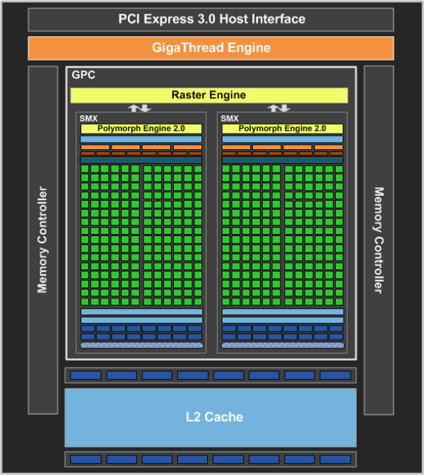
Because it’s the same GPU as with the 640M we’re looking at the same basic features and specifications, just at a higher clockspeed. All 384 CUDA cores are present, organized into 2 SMXes sharing a single GPC, making the shader frontend one quarter of a GK104 (GTX 680). Further attached to that lone GPC is a pair of ROP blocks and memory controllers, giving the GT 640 16 ROPs, 256KB of L2 cache, and a 128-bit memory bus (one half a GK104). All of this is augmented by the common features of the Kepler family, including the NVENC hardware H.264 encoder, VP5 video decoder, and PCIe 3.0 connectivity.
The clocks on the other hand are unique from any other GK107 part so far. The retail GT 640 will ship at 900MHz, faster than its OEM DDR3 counterpart but slower than the GDDR5 version. Like the laptop and OEM versions boost clock is not present, so performance is rather straightforward here. Unfortunately NVIDIA is launching with a DDR3 product here, which means that even with the 128-bit memory bus this card is going to be extremely memory bandwidth starved; at just shy of 1.8GHz it only has 28.5GB/sec of memory bandwidth. And to be honest unless there are TDP reasons we’re not really sure why NVIDIA is doing this – by the time we’re up to this many ROPs and shaders, the memory bandwidth requirements are enormous. Expect the obligatory GDDR5 version to be much faster here. In the meantime at least you get 2GB of DDR3, right?
As for physical specifications, NVIDIA’s TDP on the GT 640 is 65W, putting this card distinctly into the PCIe slot powered category. Idle power consumption on the other hand is spec’d at 15W, which if this is correct would mean that idle power is actually a bit worse than GT 440 and competing 28nm cards. In any case, functionally this makes the GT 640 the direct successor to the GT 440, which had the same load TDP. Assuming that the card’s performance isn’t held back too much by memory bandwidth limitations, this could be a very interesting card for HTPC enthusiasts thanks to the combination of a sub-75W TDP and a the various video encode/decode features Kepler brings to the table.
On that note, we finally have some solid hardware specs on the GK107 GPU itself. The official die size is 118mm2, virtually identical to the 116mm2 die size of GF108. Meanwhile the transistor count is 1.3B, more than doubling GF108 and even exceeding GF106 by over 100M transistors. This actually makes GK107 a rather large chip from a transistor standpoint; Intel’s Ivy Bridge for comparison is only 100M transistors more, and that’s a mix of CPU and GPU while GK107 is purely a GPU, which goes to show you just how big even budget GPUs are compared to CPUs/APUs.
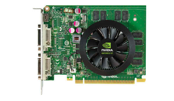
NVIDIA's Reference Design
Finally, let’s talk performance and pricing. NVIDIA’s official guidance for the GT 640 is that it should slot in just under the GTS 450, which would put its performance well above the GT 440 (which only had 4 ROPs). In practice we believe it has the potential to exceed the GTS 450 based on what we saw with GTX 680 vs. GTX 560 Ti, but at this point memory bandwidth is no doubt holding the card well back. Pricing is going to be in flux somewhat since this is a low-end part with NVIDIA’s partners doing customized designs right off the bat, but the official line is $99, making this NVIDIA’s budget market competitor (at least for the time being) and undercutting AMD’s Radeon HD 7750 by $10. However it’s unlikely that performance will be able to match the 7750 right now due to the aforementioned memory bandwidth limitations.
In any case we have samples en-route now, and we’ll have a full review on GT 640 – including HTPC usage – later this week. So until then stay tuned.


