Original Link: https://www.anandtech.com/show/5686/apples-a5x-floorplan
Apple's A5X Floorplan
by Anand Lal Shimpi on March 16, 2012 5:29 PM EST

Apple's A5X SoC
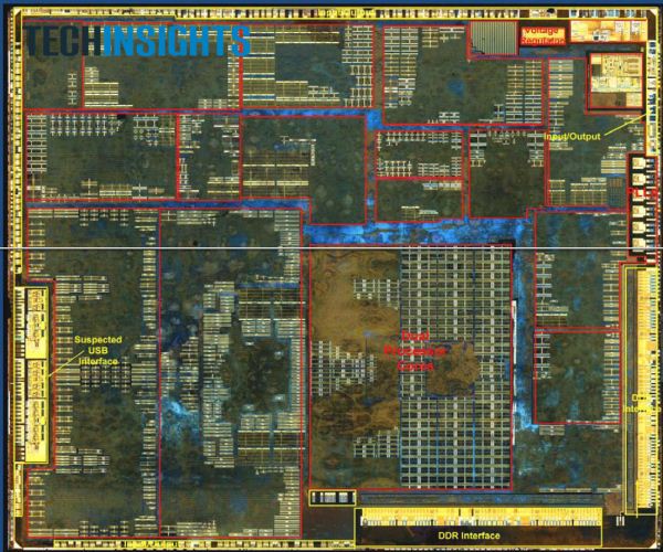
Today has been pretty exciting. Not only did we confirm the die size of Apple's A5X SoC (162.94mm^2) but we also found out that it's still built on Samsung's 45nm LP process. Now, courtesy of UBM TechInsights, we have the first annotated floorplan of the A5X (pictured above).

Apple's A5 SoC
You can see the two CPU cores (ARM Cortex A9s) as well as the additional two GPU cores (PowerVR SGX543MP4) compared to the A5 (pictured below). Note the increase in DDR interfaces, although it's unclear whether we're looking at 4x16 or 4x32-bit interfaces. It's quite possible that it's the former. Also note that Apple has moved the DDR interfaces next to the GPU cores, compared to the CPU-adjacent design in the A5. It's clear who is the biggest bandwidth consumer in this chip.


