Original Link: https://www.anandtech.com/show/5569/nvidias-rebrands-tegra-3s-vsmp-as-4plus1
NVIDIA's Rebrands Tegra 3's vSMP as 4-PLUS-1
by Anand Lal Shimpi on February 22, 2012 10:30 PM EST

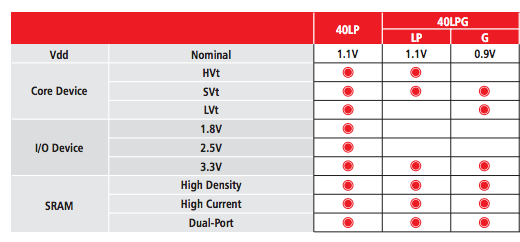
ARM Cortex A9 cores are relatively tiny and it's not too difficult to put a handful of them down on an SoC. NVIDIA did just that with its Tegra 3 featuring four ARM Cortex A9s. NVIDIA's design approach is unique in the industry in that it uses TSMC's 40nm LPG process rather than a strict LP process like many of its competitors. The G transistors are reserved for the CPU cores, while LP transistors are used everywhere else. Typically you'd build the entire SoC out of LP transistors as it's a more cost effective way to build a low power chip. NVIDIA believes that it can more efficiently hit its higher CPU frequency targets using LPG than if it used a standard LP process. G transistors are typically leakier but can scale to higher frequencies at lower voltages than LP transistors on the same process node. The tradeoff is typically that low frequency operation takes place at higher power than in an LP design.

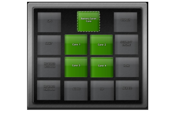
To have its cake and eat it too, NVIDIA added a fifth Cortex A9 to Tegra 3 built using LP transistors (hence the LPG process, G transistors in a sea of LP). This fifth core would only be active during the lightest of workloads and be limited in frequency (500MHz). If your phone/tablet is idle, the four higher performance A9s power down and only the fifth companion core remains active. As you unlock your phone/tablet and get to work, the fifth core eventually hands off the work to one or more of the higher clocked A9s. This dynamic architecture is what NVIDIA called vSMP.
Today NVIDIA's vSMP is getting a rebrand. As of now it's called NVIDIA's 4-PLUS-1. Expect to see a few different Tegra 3 phones announced next week at MWC brandishing NVIDIA's new 4-PLUS-1 trademark.
Source: NVIDIA Blog


