Original Link: https://www.anandtech.com/show/533

Since all of Intel’s desktop processors currently in production are based, in one form or another, on the 0.18-micron Coppermine core, they can all be expected to be capable of achieving similar clock speeds.
The part that all other 0.18-micron Intel CPUs have been derived from is the Pentium III based on the Coppermine core with 256KB of on-die L2 cache operating at clock speed. As we mentioned above, the Coppermine Pentium III is officially available in speeds ranging from 500MHz to 1GHz, although the latter speed is only available in limited quantities. As we’ve already proven in our series on Overclocking the FC-PGA, the ability of the Coppermine Pentium III core to hit such high frequencies makes overclocking the 500 – 600MHz parts very tempting since they can, with relative ease, attain very similar frequencies in the 667 – 800MHz range simply by increasing the FSB frequency.
But what does this have to do with the recently released FC-PGA Celeron processors?
The new Celeron processors are based on a variant of the Coppermine Pentium III core. Internally, they are based on a core known as the Coppermine128, which refers to the 128KB of on-die L2 cache they are outfitted with versus the 256KB that is on the regular Coppermine Pentium III core.
While there are more differences than just having 1/2 the L2 cache that’s present on the Pentium III, the most important thing to keep in mind here is that, because the new Celerons are based upon a variant of the Coppermine core, they can be expected to have similar yields and thus attain similar operating frequencies.
Taking this comparison one step further, with the exception of the extremely rare 1GHz Pentium III, the Coppermine Pentium III CPUs are available in clock speeds up to 866MHz. Presumably, Intel is seeing a high enough yield on their 0.18-micron Coppermine core to release it in quantity to the public at 866MHz. This also indicates that the Coppermine128 should also be able to hit that 866MHz mark since the core it is derived from, the Coppermine, is currently able to do just that.
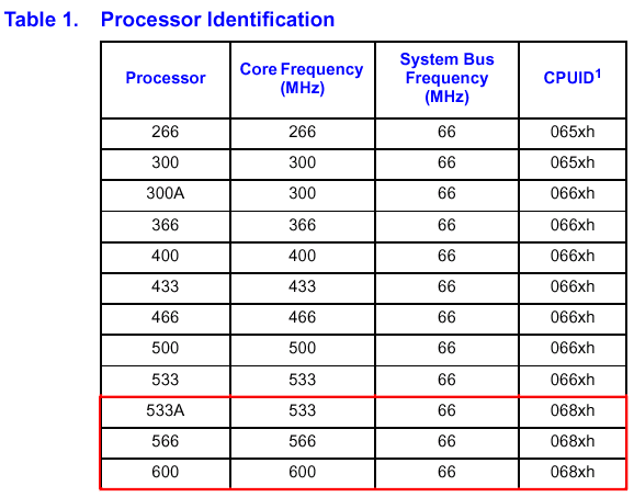
The beauty of this situation is enhanced even further when you look at the currently available FC-PGA Celerons (based on the Coppermine128 core): the 533A, 566, and 600MHz parts. These 66MHz FSB parts have clock multipliers that, when paired up with a 100MHz FSB, result in a final clock speed in the 800 – 900MHz range, which is exactly where the highest yielding Coppermine Pentium IIIs fall.
Last December, we overclocked the FC-PGA Pentium III with great success; now, let’s see how the FC-PGA Celeron fares.

A 533A Exists
Intel played down the release of the new Celeron processors as much as they could. The processors were announced on a Wednesday, not a Monday, which is the case for all major processor releases. Intel didn’t want the Celeron to turn into anything more than it was originally intended to be – a low end CPU – , which is one of the reasons you heard very little about overclocking on the day of its release.
Contrary to what the press releases said and what most of us believed, the CPUs released on March 29, 2000 included another frequency alongside the 566 and 600MHz parts that received all of the attention.
Intel also released what is known as a transitional part, designed to bridge the gap between the previous generation of processors and the current generation. For example, the original cacheless Celeron was available in 266MHz and 300MHz frequencies while the next generation Celeron with 128KB of on-die L2 cache debuted at 300MHz and 333MHz, the 300MHz part being the transitional part.
In this case, the transitional part is a little known 533MHz processor known as the Celeron 533A (much like the latter Celeron 300 was known as the 300A). The Celeron 533A is an interesting part to watch because it has a 8.0x clock multiplier which, when used with a 100MHz FSB frequency would result in an 800MHz overclock, something that is more reasonable than what a Celeron 600 with its 9.0x multiplier would result in (100MHz x 9.0 = 900MHz) since 800MHz is closer to the frequency of currently available Pentium III processors.
It has been said that beauty is in the eye of the beholder, and to most of us, the 533A is a beautiful part as it would take the place of the Celeron 300A whose 50% overclock to 450MHz is mimicked by the potential of a 50% overclock of the 533A to 800MHz.
While it’s not prominent on Intel’s site, here we have a table from Intel’s Celeron datasheet indicating the presence of a 533A as a part of the growing Celeron family.

Much more than 1/2 the Cache
When we originally got wind of the forthcoming Coppermine128 core we immediately expected them to perform virtually identically to their Coppermine counterparts since the removal of 128KB of L2 cache realistically shouldn’t result in a huge performance decrease in your everyday applications and games.
Unfortunately, shortly after the release of the new Celeron based on the Coppermine128 core (including the benchmarks that revealed that this new Celeron wasn’t the low-cost savior we had been waiting for), there was quite a bit of speculation as to why the Celeron wasn’t performing identically to a Pentium III Coppermine at the same frequency.
In our initial Celeron 600 review, we published some benchmarks that illustrated the negative effects of the 66MHz FSB on the Celeron processor, which helped to explain some of the performance discrepancies because after all, we hadn’t investigated the effects of the FSB on the Pentium III platform since the days of the original Celeron 300A to 450 overclock.
Our benchmarks proved that anywhere from 4% - 13% of the performance difference between a Celeron 600 (66MHz FSB/memory bus) and a Pentium III 600E (100MHz FSB/memory bus) was due to the 66MHz memory bus alone.
By disabling the L2 cache on both a Pentium III 600E and on a Celeron 600, we were able to determine the percentage of the performance difference attributed to the 66MHz memory bus and the remaining percentage we attributed to the 66MHz FSB frequency.
What we didn’t account for was a difference in the L2 cache of the Celeron that would cause the performance of the Celeron to be lower than an equivalently clocked Pentium III.
For starters, something must be made very clear about the Coppermine128. When Intel produces a Coppermine128-based Celeron, they don’t simply take a regular Coppermine Pentium III and disable half of the cache, and the Coppermine128 isn’t made up from the Coppermine Pentium III rejects. This we have confirmed from reliable sources inside Intel, and we’ve known this ever since the release of the Celeron.
With the aid of a program from H.Oda, we were able to confirm quite a few points of speculation about the Celeron and its relationship to its bigger brother, the regular Coppermine.
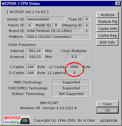
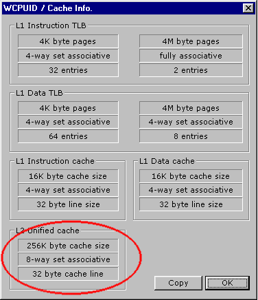
Below we have the output of H.Oda’s WCPUID program when run on a Pentium III 550E based on the Coppermine core.
And now we have the output of the same program when run on the same system, but this time we replaced the Pentium III 550E with a Celeron 566.
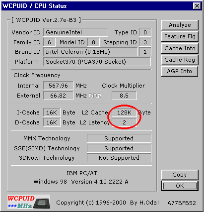
Notice anything different? The Celeron features an L2 cache latency value of 2 whereas the Pentium III features an L2 cache latency value of 0. While this could account for some of the performance difference, there is also another pretty major discrepancy between the two outputs.
Update (4/21/00): It turns out that WCPUID is in fact misreporting cache latency. According to Intel, the Coppermine128 Celeron and Coppermine Pentium III's both have the same cache latency. So much for the latency part of the theory. But there's more to cache than just latency and clock speed...

Let’s take a look at the cache data for both of these processors.
First the Pentium III 550E.
And once again, the Celeron 566.
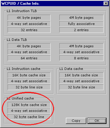
Notice anything different now? The Celeron features a 4-way set associative L2 cache whereas the Pentium III features an 8-way set associative L2 cache. This gives us missing link number two which helps to explain the Celeron’s performance.
But what does having a 4-way set associative L2 cache versus an 8-way set associative L2 cache actually mean?

L2 Cache: What it does
We often take for granted that having an L2 cache means that your system runs faster than it would if it wasn’t there, but what does that L2 cache actually do?
L2 cache, just like any other cache, acts as sort of a middle man between two mediums, in this case, your CPU’s L1 cache and your system memory (as well as other storage mediums). When the CPU wants to request a bit of data, it first searches in its L1 cache to see if it can find it there; if it does, then this results in what is known as a cache hit and the CPU retrieves it from the extremely fast, low latency L1 cache.
If it can’t retrieve it from L1 cache, it then goes to the L2 cache where it attempts to do the same – obtain a cache “hit.” In the event of a miss, the CPU must then go all the way to system memory in order to retrieve the data it needs. With the L2 cache of today’s CPUs operating at a much higher frequency and at much lower latency than system memory, if the L2 cache weren’t there or the cache mapping technique wasn’t as effective, we would see considerably lower performance figures from our systems.
4-way versus 8-way Set Associative L2 Cache
We just established that the function of the L2 cache is to provide access to commonly used data in system RAM. It does so by essentially mapping the cache lines of the L2 cache to multiple addresses in the system memory (the number of which is defined by the cacheable memory area of the L2 cache).
There are a number of methods that can be used to dictate how this mapping should occur. On one end of the spectrum we have a direct mapped cache, which divides the system memory into a number of equal sections, each one being mapped to a single cache line in the L2 cache.
The beauty of a direct mapped cache allows it to be searched relatively quickly and effectively since everything is organized into sections of equal size, but with this comes the sacrifice of hit rate because the technique does not allow for any bias toward more frequently used sections of data.
On the other end of the spectrum, we have a fully associative cache, which is the exact opposite of a direct mapped cache. Instead of equally dividing up the memory into sections mapped to individual address lines, a fully associate cache acts as more of a dynamic entity that allows for a cache line to be mapped to any section of system memory.
This flexibility allows for a much greater hit rate since allowances can be made for the most frequently used data, but at the same time since there is no organized structure to the mapping technique, searching through a fully associative cache is much slower than through a direct mapped cache.
Establishing a mid-point between these two cache mapping techniques, we have a set associative cache, which is what we’re used to with the current crop of processors available today.
A set associative cache divides the cache into various sections, referred to as sets, with each set containing a number of cache lines. With a 4-way set associative L2 cache, each set contains 4 cache lines, and in an 8-way set associative L2 cache, each set contains 8 cache lines.
The beauty of this is that the cache acts as if it were a direct mapped cache except that instead of the 1 cache line per memory section requirement, we get x number of cache lines per section of memory addresses.
This helps to sustain a balance between the pros and the cons of a direct mapped and a fully associative cache.
In the case of the Coppermine Pentium III and the Coppermine128 Celeron, the 8-way set associative L2 cache of the Coppermine Pentium III allows for a higher hit rate for the L2 cache than the 4-way set associative L2 cache of the Coppermine128 Celeron.
This combined with the fact that the 256KB of L2 cache on the Coppermine Pentium III should also theoretically result in a higher hit rate (especially with larger system memory sizes), and we have the potential for quite a performance difference between the Pentium III and the Celeron at the same clock speed.

The Motherboards
For those users that still have BX motherboards (there are quite a few of you out there), the Celerons make perfect sense since they allow you to get the most out of your setup without having to upgrade to a new 133MHz FSB platform, which would require a new motherboard in addition to your new CPU.
In spite of what you may have heard, your BX motherboard does not need to support the 8.0, 8.5, and 9.0x clock multipliers of these new Celerons in order for them to operate properly. Rather it needs to simply boast BIOS support for the processors and you should be good to go. Remember that the clock multiplier is a function of the pins on the CPU and not a function of the motherboard (i.e. the CPU can dictate what multiplier it will use, the motherboard can only attempt to “suggest” what multiplier it would like the CPU to use, and since the Celeron is clock-locked, the CPU “ignores” any suggestions made and simply uses whatever clock multiplier it was designed for).
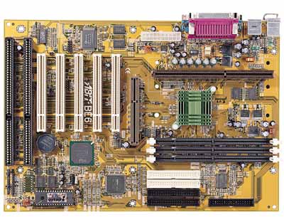
For our BX platform test bed we used an ABIT BE6, which does not currently have a released BIOS revision that officially supports the new Celeron processors. In spite of this, we did not have a problem during our tests, but this does not mean that the setup will be problem free. Our advice is to make sure that your motherboard has specific BIOS support for the new Celeron before shelling out for the processor.
For our VIA 133A platform test bed, we used the ASUS P3V4X.
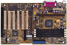
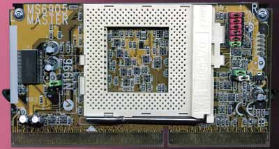
In order to get our FC-PGA Celeron to work in these Slot-1 boards, we used the Microstar MS-6905Master converter card that specifically supports FC-PGA processors. If you plan on using a converter card to get your CPU to work in a Slot-1 motherboard, be sure to get one that specifically supports FC-PGA processors; at the same time, if you plan on using your new Celeron in a Socket-370 motherboard, make sure that the motherboard supports FC-PGA processors, because in that sense, the Celeron is no different from the Pentium III.

The Candidates
We had a total of three processors for our overclocking tests: the original OEM Celeron 600 that we used for our Celeron 600 review and two OEM Celeron 566s.
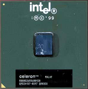
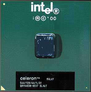
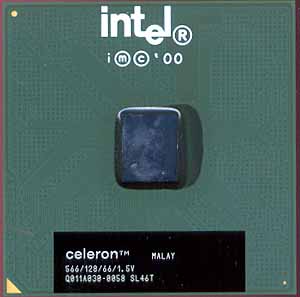
We used a default Intel heatsink/fan combo, which is what Intel ships with all boxed Celeron processors as well as all boxed FC-PGA Pentium III processors. The heatsink/fan combo isn’t the most powerful unit, but it gets the job done and does so without tacking on an additional $40 to the cost of the setup, so we were fine with using it.
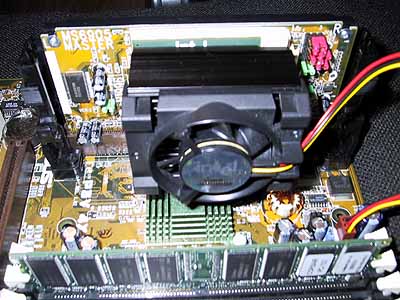
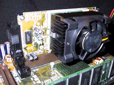
The first test was a bit disappointing. As we mentioned in our original Celeron 600 article, our 600MHz part would not hit 900MHz (100MHz x 9.0). In fact, the highest our 600MHz Celeron would reach was 750MHz, made possible using the 83MHz FSB. This was at the default voltage of 1.50v, although, in order for the system to remain just as stable as it was at 600MHz, we had to bump the core voltage up to 1.55v.
Luckily, our Celeron 566s seemed to appreciate being overclocked much more than our first 600. Both processors ran just fine at 850MHz (100MHz x 8.5) at a 1.65v core voltage setting. While this may seem a bit high, you have to keep in mind that the Pentium III 850 uses a 1.65v core voltage so this setting wasn’t exactly out of spec.
By increasing the FSB to 112MHz, we managed to get both processors to hit 952MHz, which was the highest they’d go. At 952MHz, we were clearly pushing the limits of the yield on those particular chips as we had to increase the core voltage to 1.70v to complete the performance tests and 1.75v in order to complete our stability tests over a 48 hour period.

The Test
|
Windows 98 SE Test System |
||||||
|
Hardware |
||||||
|
CPU(s) |
Intel Celeron 600 |
Intel
Pentium III 1.0EB
Intel Pentium III 866EB Intel Pentium III 800EB Intel Pentium III 733EB Intel Pentium III 667EB Intel Pentium III 600EB |
AMD
Athlon 1000
AMD Athlon 950 AMD Athlon 900 AMD Athlon 850 AMD Athlon 800 AMD Athlon 700 AMD Athlon 600 AMD Athlon 500 |
|||
| Motherboard(s) | ABIT BE6 | ASUS P3V4X | ASUS P3V4X | ASUS K7V-RM | ||
| Memory |
128MB PC133 Corsair SDRAM |
128MB
PC133 Corsair SDRAM
|
128MB
PC133 Corsair SDRAM
|
|||
| Hard Drive |
IBM Deskstar DPTA-372050 20.5GB 7200 RPM Ultra ATA 66 |
|||||
| CDROM |
Phillips 48X |
|||||
| Video Card(s) |
NVIDIA GeForce 256 32MB DDR (default clock - 120/150 DDR) |
|||||
| Ethernet |
Linksys LNE100TX 100Mbit PCI Ethernet Adapter |
|||||
|
Software |
||||||
|
Operating System |
Windows 98 SE |
|||||
| Video Drivers |
|
|||||
|
Benchmarking Applications |
||||||
| Gaming |
idSoftware Quake III Arena demo001.dm3 |
|||||
| Productivity |
BAPCo SYSMark 2000
Ziff Davis Content Creation Winstone 2000 |
|||||

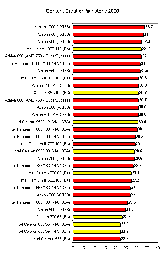
Here we see the mediocre performance of the Celeron 566/600 under Content Creation Winstone 2000 jump up to highly competitive levels simply by increasing the FSB to 100MHz resulting in the processor running at 850MHz. At 850MHz the Celeron is about as fast as a Pentium III 800E.
Increasing the once again, to FSB to 112MHz we get a Celeron running at 952MHz (up from 566MHz) and on a BX motherboard this is a very powerful setup, coming within two points of a 1GHz Athlon.

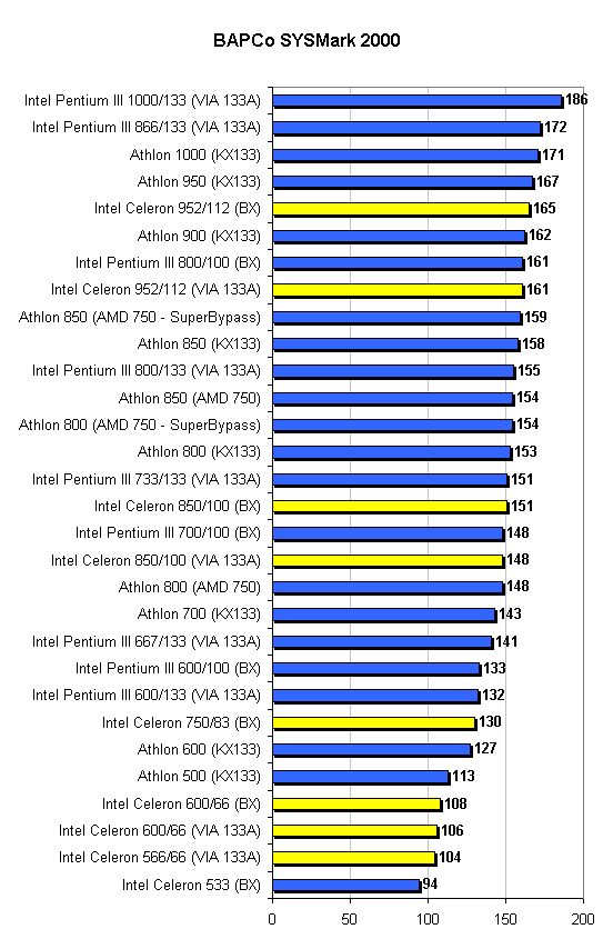
We have a similar distribution here under SYSMark 2000. The Celeron at 850MHz is a little faster than a Pentium III 700E, but this time the performance is much further from the Pentium III 800E that it was under CC Winstone 2000.
At 952MHz we have a very powerful solution once again, for $188 we have a processor that is almost as fast as a 950MHz Athlon and it's still running on a BX motherboard using the "old" 100MHz FSB.
Since you don't really need the 133MHz FSB with the Celeron, VIA's Apollo Pro 133A isn't really the ideal platform for the processor, although on some boards you would be able to increase the memory bus to 133MHz while the FSB ran at 100MHz for a performance boost.

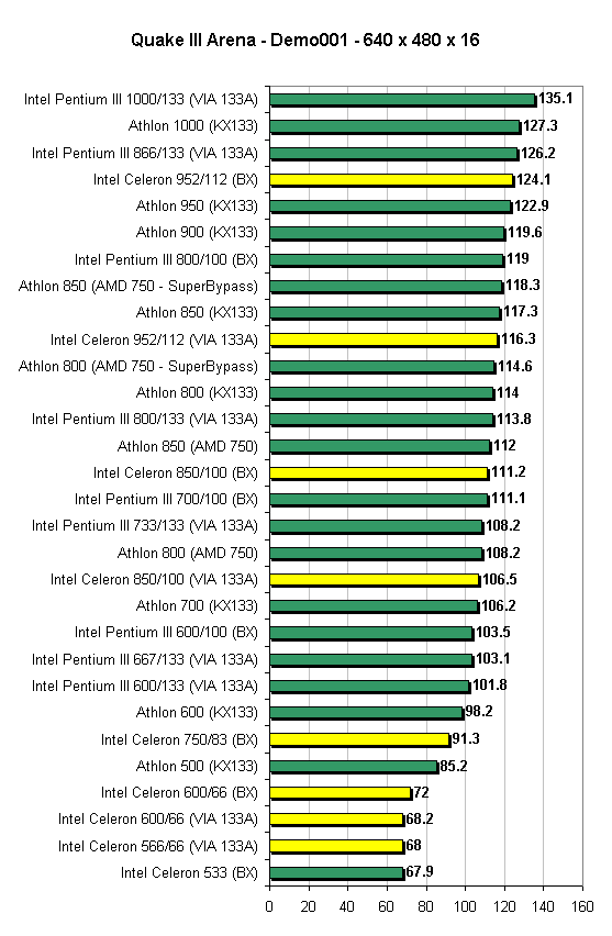
Clock for clock the Pentium III comes out on top of the overclocked Celeron, but at the overclocked speeds you're definitely getting your money's worth with the Celeron on your "old" BX board.
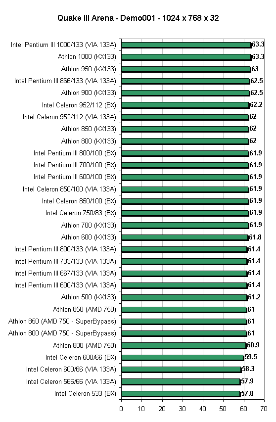
Here the GeForce is fill rate limited which explains the relatively stagnant scores.

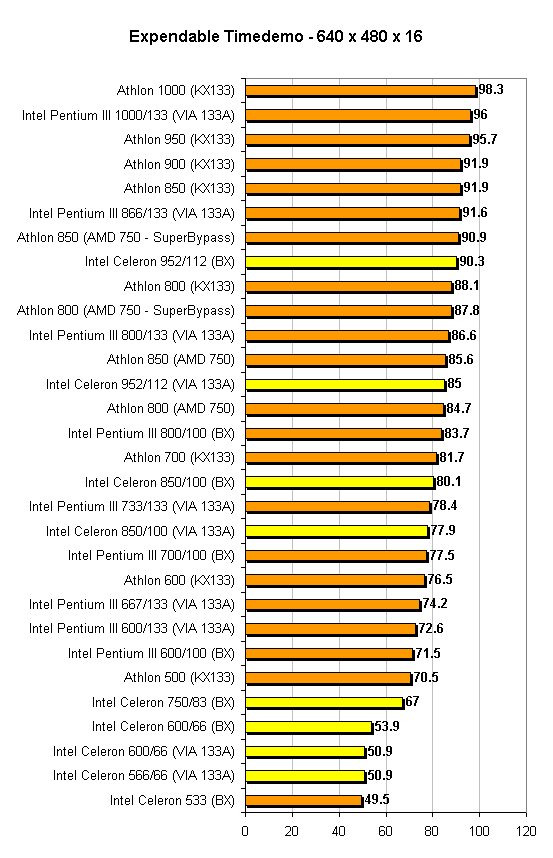
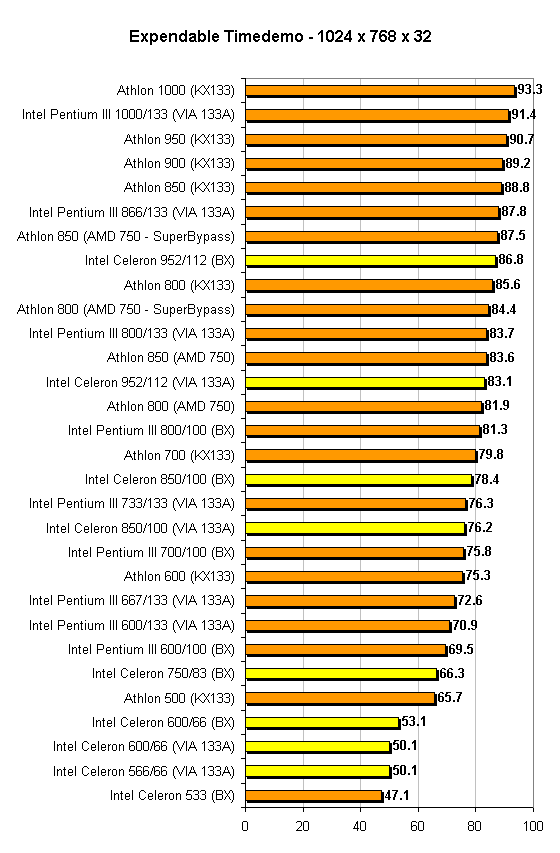
Nothing out of the ordinary here, the Celeron + BX combo still seems to be the best solution for overclocking these processors.

Conclusion
The new FC-PGA Celerons aren't as high performing as we'd like them to be, but when overclocked they can give you quite a bit of bang for your buck.
If you happen to have a BX motherboard lying around that can support the new Coppermine based Pentium III or has official support for the Coppermine128 Celeron, then picking up a 566 and pushing it to at least 850MHz wouldn't be a bad idea. If you already have a 133MHz FSB motherboard such as one based on the VIA Apollo Pro 133A chipset then you may be better off going with a FC-PGA Pentium III 550E or 600E and overclocking that to 733/800MHz. At 733MHz you'd have a slightly faster setup than the Celeron at 850MHz, depending on the price difference between the CPUs the Celeron may still be the more attractive option even in this case.
The best case scenario for the Celeron 566 seems to be running it at 952MHz on a BX motherboard. Since you only need to have the 112MHz FSB frequency at your disposal (something almost all BX motherboards support) in order to accomplish this, it shouldn't be too difficult as long as your chip can physically run at that frequency. At 952MHz the Celeron becomes a very powerful contender, and for a CPU that costs under $200 you'd have one very cost effective setup that outperforms most of what's currently out there.

