Original Link: https://www.anandtech.com/show/491
VIA Apollo Pro 133/133A Motherboard Roundup - February 2000
by Anand Lal Shimpi on February 28, 2000 1:13 AM EST- Posted in
- Motherboards
For the second time in recent history, VIA has stepped up to a leadership position in the desktop PC chipset market. The last time, if you recall, was with their MVP3 chipset, which helped keep the Super7 platform alive even while ALi’s Aladdin V solution was struggling with AGP incompatibilities.
It has usually been the case that in a market that Intel isn’t present in, VIA steps forth and takes the burden of leadership on their shoulders, and most of the time, they do a very good job at it. While it is true that, historically, VIA chipsets haven’t been as trouble free as their Intel counterparts, they have usually been able to offer their users with exactly what they wanted in terms of features.
VIA’s MVP3 chipset, for example, brought 2MB L2 cache sizes, the 100MHz FSB, and in its later stages, Ultra ATA 66 support to the Super7 platform even before Pentium III owners could get their hands on an Ultra ATA 66 enabled motherboard.
Their success in the Slot-1 market has been much less significant than what they were able to do with Super7, mainly because for the longest time, Intel’s LX and BX chipsets left very little to be desired. The BX chipset still survives today and, if it weren’t for Intel’s push away from BX, OEMs and end users alike would still be actively pursuing BX based solutions.
VIA had a very difficult time competing with the BX platform, simply because their Apollo Pro platform offered no real advantages over Intel’s solution and ended up being noticeably slower than the BX. During this time, everyone was preparing for the release of Intel’s “Camino” chipset which was supposed to offer the benefits of the BX chipset in addition to 133MHz FSB, AGP 4X and Ultra ATA 66 support. When it turned out that this chipset, now known as the i820, forced its users to adopt RDRAM as their only memory option (a very expensive one at that), the need for an alternative became evident. That alternative quickly grew to be VIA.
VIA came to the rescue of a distressed market with their Apollo Pro 133 and 133A chipsets, which offered the benefit of supporting the mainstream memory types, PC100/PC133. This is in contrast to the i820’s native support for RDRAM which, at the time of publication, was about three to five times more expensive than PC133 SDRAM. Eventually, the cost of RDRAM should come down, but until then, VIA’s Apollo Pro 133/133A solutions are the most viable alternatives for users that need official support for the 133MHz FSB, AGP 4X, Ultra ATA 66 and PC133 memory.
This roundup focuses on a total of twelve motherboards based on either the VIA Apollo Pro 133 or the Apollo Pro 133A chipset, the difference, of course, being that the 133A chipset supports AGP 4X while the 133 features only AGP 2X support. The motherboards included in this roundup are the ABIT VA6, ASUS P3V4X, AOpen MX64, ECS P6BAP-A+, ECS P6BAP-Me, ECS P6VAP-Me, EPoX 3VCA, FIC KA-11, Gigabyte GA-6VX-4X, Gigabyte GA-6VX7-4X, Shuttle AV64 and the Tyan Trinity 400.
The Chipset
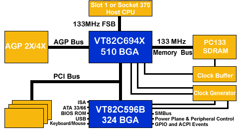
 The VIA Apollo Pro 133/133A
chipset is a unique entity primarily because of its flexibility as a chipset.
Motherboard manufacturers can easily adopt their BX designs for use with the
133, and with a bit more work they can modify it for the 133A.
The North Bridge of the Apollo Pro 133 chipset is the VT82C693A, the ‘A’ at the end of the string denoting that it supports the 133MHz FSB frequency which its predecessor, the VT82C693 did not support.
With its 133MHz FSB support, there is also support for the 1:2 AGP clock ratio, meaning that the AGP bus can be set to operate at 1/2 the FSB frequency. This is in addition to the 1:1 and 2:3 ratios that were brought over from the old Apollo Pro Plus and are also supported by the Intel BX chipset. Other than the i820 and i810E chipsets, the Apollo Pro 133 is the only other chipset to support the 1:2 AGP clock ratio.
The 693A supports AGP 2X as well as up to 2GB of SDRAM or Virtual Channel SDRAM which can operate at the FSB frequency – 33MHz, FSB + 33MHz or at a frequency equal to that of the FSB.
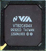
The VIA Apollo Pro 133A makes use of the VT82C694X North Bridge, otherwise known as the 694X. The 694X differs from the 133’s 693A North Bridge in that it supports AGP 4X, which increases the pin count of the chip. This unfortunately means that the 694X cannot be dropped into a 693A motherboard design without any modifications to the layout itself.
Other than the AGP 4X support, the 694X’s feature set is identical to the 693A since they are essentially the same chip.
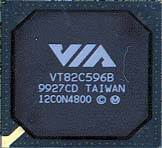 The South Bridge that can
used with the 693A and the 694X isn’t North Bridge dependent, meaning that a
motherboard manufacturer could choose to use the 693A North Bridge with the
same South Bridge as a 694X based board.
The two options motherboard manufacturers have when choosing a South Bridge are the 596B or the 686A. The 596B is known as the Mobile South Bridge and VIA uses the term Super South Bridge to define the 686A. Taken from our VIA Apollo Pro KX133 Review (the KX133 has the same South Bridge options), here are some of the benefits the 686A offers over the 596B and other South Bridge solutions:
· Inter-operable with VIA and other Host-to-PCI Bridges – As we just finished discussing, the fact of the matter is that the 686A can be used on a number of VIA chipset implementations, thus helping to keep costs down since VIA only has to manufacture one chip that can be implemented on a number of motherboard designs.
· Integrated PCI-to-ISA Bridge – This feature, present on the now old Intel piix4 and piix4e South Bridges but absent on the i820 and i810(E) chipsets, allows for the implementation of ISA slots on a motherboard that uses the 686A without having to use an external PCI-to-ISA Bridge. This helps save PCB space and cut costs. On the reverse side of things, ISA slots are quickly dying, so this feature is becoming less of a necessity.
· Ultra ATA 33/66 PCI EIDE Controller – Ultra ATA 33 has just recently began to be saturated by the latest 7200 RPM IDE hard drives, so Ultra ATA 66 support is definitely a desired feature. While Intel is supposed to announce ATA-100 support in the near future, it will be a while before hard drives saturate the 66MB/s peak transfer rates of the Ultra ATA 66 specification.
· Integrated Super I/O Controller – Unique to the 686A, the integrated Super I/O controller takes care of all of the basic I/O needs of a motherboard. It provides the serial, IR, and parallel ports as well as the Floppy Disk Controller for the motherboard. Why is this so special? Well, currently no Intel chipset has these features integrated into any part of the chipset, meaning they have to resort to an external I/O controller to provide these functions. This external controller not only occupies PCB area on the motherboard it also adds the cost of another chip to the price of the motherboard. This is a feature the AMD 756 South Bridge does not support, one reason why many motherboard manufacturers chose to go with the 686A over the AMD 756 in their Athlon motherboard implementations.
· AC’97 & MC’97 Support – VIA based motherboards that take advantage of the Audio Codec ’97 support of the 686A South Bridge will feature an AC’97 controller placed on the motherboard that drives an integrated audio output while supporting the use of the AMR (Audio Modem Riser) slot for higher quality audio or modem support. The reason for the use of the AMR slot is to place the more sensitive components on an AMR slot so that motherboard manufacturers don’t have to increase the production time of their products because of the certification required for sensitive analog components such as those on modems or higher quality audio devices. This is also why, in spite of the presence of the AMR slot, the motherboard manufacturers will go ahead and include audio inputs/outputs on the motherboard itself, so they don’t have to worry about the certification time required by an AMR card in order to ship their boards to OEMs with integrated sound.
Remember that these AC’97 controllers depend on the host CPU to do most of the work associated with their particular tasks, but because of this they add a negligible amount to the final cost of the motherboard.· Integrated Hardware Monitoring – Once again, by integrating hardware monitoring onto the 686A South Bridge, VIA helps to cut motherboard manufacturing costs by removing yet another chip from the PCB. Most motherboards use an external chip to provide hardware monitoring functionality which takes up PCB space and adds the cost of the chip to the motherboard. The integrated hardware monitoring can monitor 5 voltages (including the voltage supplied to the 686A chip itself), three temperatures (including the temp of the 686A) and two fans.
· Universal Serial Bus Controller – The 686A’s USB controller goes one step above Intel’s current USB implementation by allowing support for up to 4 USB devices.
In the end, the 686A South Bridge helps to integrate three commonly external chips (I/O Controller, Hardware Monitoring Controller, and South Bridge) into one chip. This helps to bring the cost of motherboards based using the 686A down to costs lower than what the implementations based on the 596B placed them at. The 686A is a better overall solution than the 596B for a motherboard manufacturer yet there are still some motherboard manufacturers that use the old 596B South Bridge.
What to look for in an Apollo Pro 133/133A Motherboard
In the past few years, motherboards have increased in quality, reliability and performance but the main things you look for in a motherboard haven’t really changed. You look for stability, expansion and features. Cost is often a concern, but for the most part, motherboards in the same category (such as those based on the 133A chipset) go for approximately the same cost.
One consideration that hasn’t been a factor in the past is performance. Generally speaking, motherboards of the same type (i.e. BX boards) should perform within a few percent of one another. However, this is not the case with 133/133A based motherboards as there is quite a bit of tweaking that can be done on the BIOS side of things to improve performance as well as stability, so keep in mind that in this roundup performance is a factor.
Form Factor & SizeVIA’s chipsets have always been aimed at the desktop and/or low-cost market, so you’ll be hard pressed to find a 133A based motherboard aimed at anything in the workstation, much less the server, market. Because of this, 133A boards will be available in two form factors, ATX and microATX with no WTX or extended ATX based designs.
The nature of the 133A dictates that it will be a direct competitor to Intel’s 820 chipset and a successor to the Intel BX; this results in the most common layout for a 133A board being the standard ATX form factor. At the same time, the low-cost nature of the chipset and the highly integrated 686A Super South Bridge option make producing microATX 133A boards very attractive to motherboard manufacturers.
The i820 chipset is simply too expensive of a solution to make it into many microATX designs that OEMs will buy, but the 133A chipset, with its SDRAM support makes for a very desirable alternative for OEMs looking to put together some sub-$1000 microATX systems.
Size is also a big issue with motherboards, especially if you’re going to be putting together a system in a cramped case where maintaining sufficient airflow can quickly become an issue for cooling and overclocking.
With the transition to FC-PGA 370 designs, most manufacturers will be promoting their Socket-370 boards more than their Slot-1 solutions. In an effort to help make the transition as smooth as possible, some manufacturers will be outfitting motherboards with both Socket-370 and Slot-1 CPU interfaces, which obviously takes up some extra space on the PCB.
Standard ATX Socket-370 motherboards are oftentimes just as large, if not larger, in terms of surface area, as their Slot-1 counterparts because of the fact that a Slot-1 connector actually occupies less space since it’s just a thin straight line versus a Socket-370 connector, which is more of a square.
Luckily, because of the target market of the Apollo Pro 133/133A chipsets, finding a board based on these chipsets that exceeds the standard ATX specification with its dimensions should be a difficult task. The only decision you’ll have to make here is whether you want a microATX or a regular ATX motherboard and choose your case accordingly.
Expansion Slots
The flexibility of the Apollo Pro 133/133A chipsets is seen in the number of different expansion slot configurations motherboard manufacturers will use with the chipsets. The reason for this flexibility is because that, with the 686A Super South Bridge and its integrated ISA bridge, the costs associated with adding ISA slots to a motherboard layout are reduced to the costs of the physical slots themselves. This is in contrast to the i820 chipset, for example, where an extra PCI-to-ISA bridge must be placed on the motherboard which occupies expensive space on the PCB.
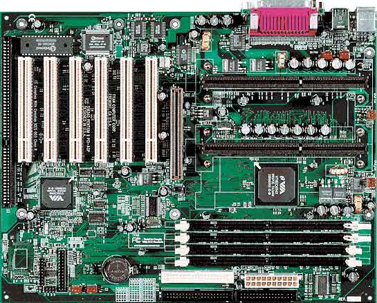
We have seen 133A boards with 1, 2 and even 3 ISA slots as well as boards with a full 6 PCI slots. Keep in mind that if you have a motherboard outfitted with 6 PCI slots, one of those six will act as a slave slot unless the motherboard manufacturer has made provisions to support 6 master slots. As of the time of publication, only Microstar had been shipping motherboards with this PCI arbiter chip, but since there is a relative lack of demand for 6 PCI master slots, it is unlikely that you’ll see more manufacturers adopt such a provision.
The beauty of the flexibility of the 133A chipset is that users with legacy ISA cards can find a motherboard with enough ISA slots to accommodate their needs but at the same time those users that have made the shift to PCI peripherals should have no problem finding a motherboard with at least 5 PCI slots.
The downside to all of this is that without more motherboard manufacturers adopting PCI-only layouts, it will take even longer to get rid of legacy ISA slots and ISA peripherals.
Another interesting situation with 133A based boards is that not all of them feature AMR slots. This is the exact opposite from the i820 motherboard situation where every board features an AMR slot.
The explanation behind this is two fold:
1) Some motherboard manufacturers are still using the 596B Mobile South Bridge, which does not feature an AC’97/MC’97 controller, which prevents them from outfitting boards based on the 596B with an AMR slot
2) The AMR slot was never intended to be a retail option, only an option for OEMs. The idea of purchasing AMR upgrades, etc… after market is something that was never intended as a possible use for AMR. VIA isn’t as strict as Intel in terms of enforcing technological implementations on motherboard designs, and thus when a motherboard manufacturer refuses to make use of an AMR slot, VIA doesn’t see a huge problem with that.
A combination of those two factors is keeping AMR slots off of quite a few of VIA based motherboards. Motherboard manufacturers will outfit their boards with AMR slots if their OEMs demand the option, but unless they have a specific need to they will not
AGP 4X & AGP Pro
As we mentioned in The Chipset section of this roundup, the main difference between the Apollo Pro 133 and the Apollo Pro 133A chipsets is that the latter supports AGP 4X while the former boasts only AGP 2X compliance.
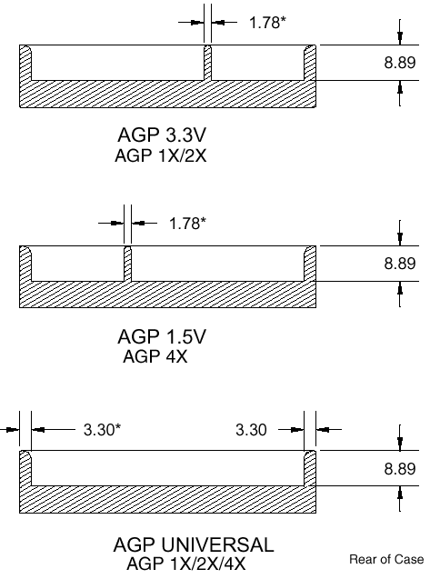
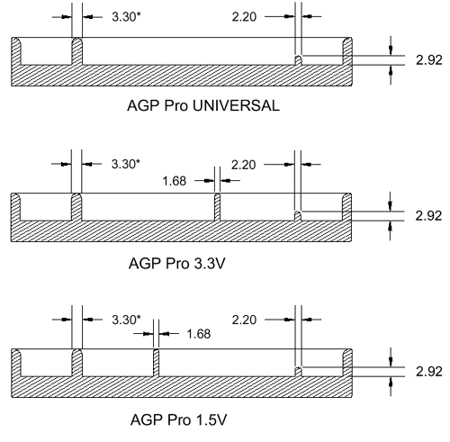
In spite of this, most motherboard manufacturers are opting to use universal AGP connectors on all of their motherboards, regardless of whether or not they support AGP 4X. The universal AGP connector features no 1.5v keying for AGP 4X or 3.3v keying for AGP 1X/2X cards. This allows the slot to accept all AGP 1X, 2X and 4X compliant cards, although in the case of motherboards based on the 693A North Bridge, only transfer modes up to AGP 2X are supported.
Out of the twelve motherboards we rounded up, two of them (both of which used the 693A North Bridge) featured slots keyed for AGP 1X/2X cards while the rest featured universal AGP slots.
AGP Pro is another trend we have been noticing with motherboards, but the AGP Pro slot is reserved mainly for workstation level systems that have graphics cards which require the additional power supplied to them by an AGP Pro slot. Because of this, it is highly unlikely that you will see an AGP Pro equipped 133/133A motherboard, but at the same time, we have yet to see any video cards that absolutely require the use of an AGP Pro slot.
Integrated Audio/Telephony Codecs
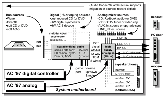
One of the benefits, for manufacturers, using the 686A Super South Bridge boasts is that it features an integrated AC’97 Digital Audio Controller and an MC’97 Modem controller that enable low-cost, software based Audio and Modem solutions at a minimal cost to the manufacturer. These two features aren’t supported by the 596B Mobile South Bridge, so motherboards based on that South Bridge naturally will not feature them.
The integrated AC’97 controller still requires the use of an external Audio codec, but after the codec is placed on the motherboard the physical audio connectors can be placed on the board itself.
In order to take advantage of the integrated MC’97 controller, you must use an AMR card, but as we mentioned earlier, AMR cards were never intended for public consumption but rather as an option for OEMs or system integrators.
The integrated AC’97 and MC’97 controllers of the 686A Super South Bridge is a definite advantage for OEMs and system integrators, but for most AnandTech readers motherboard manufacturers better be glad that the codecs don’t cost much to implement on a motherboard design, otherwise there would be hell to pay, especially from the thousands of users that don’t use AMR or software based audio which can eat up a decent part of your CPU time.
Memory Support
The Apollo Pro 133 and 133A share the same memory controller, which supports two major types of memory: SDRAM and Virtual Channel SDRAM. Unfortunately absent from this short list is DDR SDRAM, and according to VIA we won’t see support for that until later this year but it will be in the form of a P6-bus motherboard platform, meaning that it will work with the Pentium III.
The 693A and 694X North Bridges support both PC133 and PC100 SDRAM as well as VC100 and VC133 Virtual Channel SDRAM. The way the chipset goes about supporting more than one clock frequency of the same memory type is by allowing the user to clock their memory at 33MHz faster or 33MHz slower than their FSB frequency or equal to their FSB frequency if they have memory capable of running at that speed.
This allows a user with PC100 memory to run their memory at 100MHz while their FSB operates at 133MHz (133MHz – 33MHz = 100MHz) while a user with PC133 memory can run their memory at 133MHz even if their FSB is only running at 100MHz. There are obviously more combinations than this alone, but it is up to the motherboard manufacturer to make sure that support for these combinations is provided for.
Ideally, motherboard manufacturers should allow a user to set his/her memory bus equal to the FSB, FSB + 33MHz or FSB – 33MHz regardless of the FSB setting. This would give the user the opportunity to theoretically clock their memory at 166MHz while their FSB runs at 133MHz. Unfortunately, we have yet to see any memory capable of reliably operating at this frequency which makes this more of a “wouldn’t that be cool” than a reality.
The Virtual Channel SDRAM support of the 133/133A chipsets is an interesting feature, but it is a relatively unused feature due to the lack of availability of VC-SDRAM modules in the market today. It is unlikely if this will change as VC-SDRAM is nothing more than an intermediate solution to resolve the issues of memory bandwidth limitations until a more bandwidth friendly standard, such as DDR SDRAM, can be adopted and implemented into motherboard designs.
In addition to the relatively unavailability of VC-SDRAM, our tests have concluded that the performance of VC-SDRAM isn’t all that it’s cracked up to be. It is barely faster than SDRAM in most situations and in some cases it is actually slower than regular PC100 or PC133 SDRAM, something which is most likely the fault of a flawed VC-SDRAM implementation in VIA’s memory controller.
Needless to say (it’s something we can’t say enough), VC-SDRAM isn’t something you should lose sleep over. It’s not something that you’re missing out on, simply because the performance isn’t there. While the technology behind it is definitely interesting, it’s not worth the trouble at this point in time.
Dual Processor Support
Until very recently, it was unclear as to what sort of dual processor support these chipsets carried. At last year’s Fall Comdex, Tyan gave us a demonstration of a ~$100 dual processor motherboard based on the 694X chipset. The reason for its low cost was because of the low cost of the 694X chipset itself and because of the fact that the 694X features an integrated SMP ASIC that eliminates the need for an external chip to be used in order to enable SMP support.
While the board didn’t make it into this roundup, we will be sure to provide a review of it in the near future.
Hardware Monitoring
Hardware monitoring is one of those often overlooked features of a motherboard. While it's not a necessary component, it can help prevent catastrophic failures or provide valuable information when troubleshooting a problem. For example, you can set an alarm to go off if they system is overheating or a fan has stopped. Some software will even shutdown the system automatically under such circumstances. Many motherboards even throttle back the CPU speed if things start to heat up too much. All this in the name of protecting your system and your data.
One of the beauties of the 686A Super South Bridge is that it features an integrated hardware monitoring solution, meaning that an external chip isn’t necessary. So this section is mainly for the hardware monitoring options that manufacturers can use with the 596B Mobile South Bridge.
Most hardware monitoring chips out there allow for the measurement of system voltages, CPU fan speed, system temperature, and CPU temperature. However, each chip out there has different features when you get into the nitty gritty. Complicating things further is the fact that it is up to each individual motherboard manufacturer to implement those features and every implementation ends up being slightly different. Let's take a look at the different hardware monitoring solutions out there, along with some of the possible implementation issues they may face.
Winbond 83781D
The Winbond 83781D was the first popular hardware monitoring chip on the market. It's actually still used by a few companies that haven't bothered to upgrade to the newer editions of this chip. The 83781D provides monitoring for 5 positive voltages, 2 negative voltages, 3 remote temperatures, and 3 fan speeds. A case open input is also available for added security.
Those 7 voltage inputs are typically used to monitor +/-5V, +/-12V, +3.3V, and Vcore. The remaining voltage input is often used to measure VTT, +5Vsb (standby), Vbat (battery), or the Vcore of a second CPU. The 83781D features five Voltage ID (VID) inputs that read the VID pins of the CPU in order to automatically compensate for different Vcore values from different processors.
The three remote temperatures are read via external thermistors. A thermistor is a device whose resistance varies proportionally to its temperature. These thermistors can be mounted anywhere on the motherboard, but typically at least one is used to monitor the CPU temperature. A CPU thermistor would be mounted either in front of the CPU slot or inside the CPU socket. Some motherboards offer headers that allow you to hook up your own thermistor anywhere in the case. The reaction time and accuracy of the thermistor varies by brand and model.
Winbond 83782D
The 83782D is the success to the 83781D and offers one key advantage - the ability to read CPU temperature from the on-die thermal diode of any 0.25 micron or 0.18 micron Intel CPU. Reading from the on-die thermal diode offers the most accurate CPU temperature possible.
Otherwise, the 83782D offers similar specs - monitoring for 9 voltages, 3 temperatures, and 3 fan speeds. Case intrusion is still supported as is the CPU VID detection of the correct Vcore. Those 2 additional voltages allow for monitoring of just about every voltage in the system, usually +/-5V, +/-12V, +3.3V, Vcore, VTT, +5Vsb, and Vbat.
Most motherboard manufacturers that choose the 83782D are wise enough to read the CPU temperature from the on-die thermal diode. However, a surprising number still use this in conjunction with an external thermistor near the CPU slot/socket, which leads to slower reaction time for temperature changes.
Winbond 83783S
The Winbond 83783S is simply a stripped down version of the popular 83782D chip and differs primarily in the number of voltages monitored - 6 instead of 9. Typically, this is used to monitor +/-5V, +/-12V, +3.3V, and Vcore. You can still read CPU temperature from the on-die thermal diode, but once again, many manufacturers are still using thermistors. Case intrusion is still supported as is the CPU VID detection of the correct Vcore. Motherboard manufacturers choose this chip over the other Winbond models to cut costs just a bit.
Winbond 83627HF
The 83627HF is actually primarily an I/O controller that happens to feature hardware monitoring support. On the hardware monitoring side, it's very similar to the W83782D. It offers the same total of 9 voltage inputs, 3 fan speeds, and 3 thermal inputs. Once again, CPU temperature can be read from the on-die thermal diode, the VID detection of Vcore, and case intrusion are all supported. Since this chip is quite new, most implementations make use of the CPU's on-die thermal diode, but continue to watch out for thermistors for monitoring CPU temperature. The 83627HF does add one interesting feature - the ability to control fan speed as system/CPU temperature varies. Expect this chip to become extremely popular because its price premium over a standard I/O chip without hardware monitoring is minimal.
Winbond 83697HF
Like the 83627HF, the 83697HF is also primarily an I/O controller with integrated hardware monitoring features. It's a stripped version of the 83627HF with the main differences being a total of 8 voltages monitored, 2 thermal inputs, and 2 fan speeds. Once again, CPU temperature can be read from the on-die thermal diode, the VID detection of Vcore, case intrusion, and fan speed control are all supported. Since this chip is quite new, most implementations make use of the CPU's on-die thermal diode, but continue to watch out for thermistors for monitoring CPU temperature. We also expect this chip to become quite popular as it’s even cheaper than the 83627HF.
Jumperless CPU & Voltage Configuration
Ever since ABIT and QDI produced the first ever motherboards with a fully jumperless CPU and voltage setup, the goal of many manufacturers has been to bring that level of ease of use and operation down to their products as well.
The AWARD BIOS Setup v6.00 features a built in CPU Frequency & Voltage adjustment setup, it is the job of the manufacturer to take advantage of the option and enable it on their motherboards. So there is no excuse for a motherboard that uses the AWARD v6.00 BIOS not to have a jumperless CPU & voltage configuration.
There are certain features which you should be able to adjust, and those features do take a little more work on the part of the manufacturer to implement especially in a jumperless configuration.
One of the features we mentioned earlier in the article, which is very important, is the ability to adjust the memory clock regardless of the FSB frequency selected. Being able to choose from one of three options: FSB, FSB – 33MHz and FSB + 33MHz for your memory bus frequency is a very useful feature and something that should be controlled within the BIOS setup.
The number of FSB frequencies supported is a function of the particular clock generator on the motherboard, but being able to support the entire range of FSB frequencies is something that must be implemented within the BIOS setup if the board boasts a jumperless configuration.
BIOS Setup & Support
Another often overlooked feature is a motherboard’s BIOS setup utility. All of the boards we rounded up here use a BIOS manufactured by either AMI or AWARD.
In the lab, we prefer the AWARD 6.00PG setup utility; however, the most important consideration is how thorough the setup utility covers the features and options of the chipset. Arguably of equal worth to any motherboard is how well the manufacturer keeps the BIOS up to date and takes care of problems that are brought to their attention.
The only way to truly measure this is by visiting the manufacturer’s support section and taking a look at BIOS updates for other motherboards as well as ask around on online message board forums and newsgroups.
Manufacturer Support
One of the most important features when dealing with any motherboard is the support that backs it. Support is available not only in the form of written documentation but through the manufacturers’ web site in the form of driver downloads, BIOS updates, and more. It’s always good practice to check around motherboard manufacturers’ web sites in order to see the frequency at which they update their BIOSes (especially for older motherboards).
There is no replacement for word of mouth passed on by other users; it seems like motherboards don’t inspire the same tension that video cards and CPUs do when it comes to asking for advice. Asking the question "3dfx or NVIDIA?" or "AMD or Intel" in most newsgroups will end up in a flame war, whereas asking for personal experiences with a particular motherboard manufacturer online will usually give you a good set of responses to help gauge your motherboard manufacturer’s support rating. The AnandTech Motherboard Discussion Forum on the AnandTech Forums is an excellent place to ask about individual experiences with motherboard manufacturers.
The Candidates
Over the next few weeks you will see individual reviews of all of the motherboards covered in this roundup, and as we publish them we will add the links to the actual reviews in this section, but until then, here are brief looks at all of the motherboards present in this roundup.
The motherboards included in this roundup are the ABIT VA6, ASUS P3V4X, AOpen MX64, ECS P6BAP-A+, ECS P6BAP-Me, ECS P6VAP-Me, EPoX 3VCA, FIC KA-11, Gigabyte GA-6VX-4X, Gigabyte GA-6VX7-4X, Shuttle AV64 and the Tyan Trinity 400.
ABIT VA6
|
Motherboard Specifications |
|
| CPU Interface |
Slot-1
|
| Chipset |
VIA Apollo 133
VIA 693A North Bridge VIA 686A South Bridge |
| L2 Cache |
N/A (on-chip)
|
| Form Factor |
ATX
|
| Bus Speeds |
66 / 75 / 83
100 / 105 / 110 / 112 / 115 / 120 / 124 133 / 140 / 150 |
| Voltages Supported |
1.50v - 1.80v (in 0.05v increments)
|
| Memory Slots |
3 168-pin DIMM Slots
|
| Expansion Slots |
0 AMR Slots
1 AGP Slot 5 PCI Slots (5 Full Length) 2 ISA Slots (1 Shared / 1 Full Length) |
| AC'97 |
VIA VT1611A
|
| BIOS |
AWARD BIOS 4.60PG
|
ABIT’s VA6 was one of the more highly anticipated motherboards in this roundup, but our experience with the board was tainted as we received a bad test sample.
Unfortunately, we weren’t an isolated case, quite a few users have actually purchased bad boards like the one we were sent for review. It is one thing for a manufacturer to send us a bad motherboard for review, but it’s another to see people spending their hard earned money on a bad product. Luckily, there have been increasing cases of users satisfied with their VA6 boards, indicating that ABIT has corrected the issues present in the batch of boards that were sub-par in terms of quality. At the same time, unless all the bad boards have been recalled by ABIT, there is still a chance that you could end up with a bad VA6.
Assuming that you do end up with a good VA6, what benefits does the VA6 offer over the competition? Actually very little, which is odd considering that ABIT has usually been known to throw in a few features that the rest of the market hadn’t thought of.
The VA6 does offer ABIT’s fully jumperless SoftMenu setup, but, unfortunately, it’s not the same SoftMenu III jumperless setup that we’ve seen on their latest BX boards such as the BF6.
While reviewing the VA6 we came up with the theory that the VA6 was little more than a BH6 modified for use with the Apollo Pro 133 chipset, especially since the layout was virtually identical to the old BH6 and ABIT opted to go with the 693A North Bridge which is pin compatible with the BH6’s 443BX North Bridge allowing ABIT to simply drop in the 693A into the BH6 design with minimal effort to produce the VA6.
Luckily, ABIT made the smart decision of using the 686A South Bridge; the only thing that doesn’t make sense is that they’re using the older 693A North Bridge. ABIT has told us that they will be releasing a new board based on the 694X based on a new motherboard design, but that will not be in the immediate future.
Until ABIT’s next solution hits the streets, there’s no real reason to consider ABIT as a contender for the top 133/133A spot since there some clearly superior solutions out there.
ASUS P3V4X
|
Motherboard Specifications |
|
| CPU Interface |
Slot-1
|
| Chipset |
VIA Apollo 133A
VIA 694X North Bridge VIA 596BSouth Bridge |
| L2 Cache |
N/A (on-chip)
|
| Form Factor |
ATX
|
| Bus Speeds |
66 / 68 / 75 / 80 / 85 / 90 /
95 / 100 / 103 / 105 / 110
112 / 115 / 116 / 118 / 120 / 124 / 126 / 130 / 133 / 135 138 / 140 / 142 / 144 / 146 / 148 / 150 / 155 / 160 / 166 |
| Voltages Supported |
1.30v - 1.80v (in 0.05v increments)
|
| Memory Slots |
4 168-pin DIMM Slots
|
| Expansion Slots |
0 AMR Slots
1 AGP Slot 6 PCI Slots (6 Full Length) 1 ISA Slots (1 Shared / 1 Full Length) |
| AC'97 |
N/A
|
| BIOS |
AWARD BIOS 6.00PG
|
Just as ABIT has somewhat of a cult following, ASUS has a similar claim to fame.
While the name ASUS wasn’t associated with extreme overclocking when the ABIT BH6 was stealing the lime light during the days of the Celeron 450A combo, ASUS actually introduced the overclocking market to the 83MHz FSB frequency with their T2P4, arguably the first motherboard to ever support the 83MHz FSB frequency.
The P3V4X is the best solution for overclockers as it features a total of 32 FSB settings, and unlike other motherboards that claim support for an enormous amount of FSB settings, the P3V4X actually offers settings that can be useful to overclockers, especially when you’re overclocking the FC-PGA.
The board features ASUS’ JumperFree setup and configuration utility that resides within the board’s AWARD BIOS setup. Using the JumperFree setup you can adjust the memory clock, FSB frequency, and the voltage supplied to the CPU. The JumperFree setup will automatically select the AGP clock ratio based on your FSB selection in the BIOS, but if you want to adjust this option or any other setting manually, the P3V4X features its own set of override settings on the board that are controlled by a block of 10 dip-switches.
While ABIT may be known for their SoftMenu setup, the P3V4X puts the VA6’s SoftMenu to shame with its plethora of options that will satisfy the overclocker in all of us.
The P3V4X was one of the most reliable motherboards out of the roundup. While that would normally not be a problem at all, the reason behind its stability is what we’re questioning. ASUS has always been known for producing high quality products, and they have been known to sacrifice performance in favor of selling a more reliable product. This seems to be the case with the P3V4X as it was extremely stable in our tests, but came in last place under the gaming performance tests with a score of 78 fps under Quake III versus the 120 fps of the Gigabyte GA-6VX-4X, the fastest board in our roundup.
The only explanation for the board’s low performance under Quake III, yet seemingly normal performance under CC Winstone 2000 and SYSMark 2000, is that ASUS tweaked the board’s BIOS for stability, not performance. One setting that could have impacted the performance of the board was a setting that we originally ran into on the Tyan Trinity 400, the CPU IOQ Size option that was present in the BIOS setup. This option controls the In Order Queue size value of the chipset and should be, by default, set to a value of 4 for optimal performance.
The initial revisions of the Tyan board had this default set to 1 in order to improve stability; unfortunately, this made them take a huge performance hit under games such as Quake III. The later revisions of the board, including the latest Rev. D board that we tested have the option set to 4 by default which boosts performance significantly with seemingly no impact on stability.
Setting the CPU IOQ Size to 1 on the Tyan board resulted in Quake III performance closer to what we found with the ASUS P3V4X, further supporting our theory that ASUS simply set the default to 1 but didn’t allow for an option to change the setting in the BIOS. We will be in contact with ASUS to see if they are working on a BIOS update to resolve this situation because if they do release an update, the P3V4X can easily take the AnandTech Editor’s Choice Award for best overall 133A board in this roundup.
Another complaint we have about the P3V4X is that ASUS chose to go with the 596B South Bridge instead of the highly integrated 686A Super South Bridge. This is quite disappointing since the 686A would help to cut down on the cost of the board because it does feature an ISA slot and an ISA bridge to support that slot, the latter would be integrated into the 686A had they chosen to go with it.
For those of you that aren’t heavy gamers, the P3V4X performs perfectly fine in all business and content creation applications, and it is one of the most stable 133A boards we have tested. Hopefully with a BIOS update, ASUS can get their performance up to par with the top few boards in this roundup.
AOpen MX64
|
Motherboard Specifications |
|
| CPU Interface |
Slot-1
|
| Chipset |
VIA Apollo 133A
VIA 694X North Bridge VIA 686A South Bridge |
| L2 Cache |
N/A (on-chip)
|
| Form Factor |
microATX
|
| Bus Speeds |
66
/ 75 / 83
100 / 105 / 110 / 112 / 115 / 120 / 124 133 / 140 / 150 |
| Voltages Supported |
Auto Detect - 1.30v - 3.5v
|
| Memory Slots |
3 168-pin DIMM Slots
|
| Expansion Slots |
0
AMR Slots
1 AGP Slot 3 PCI Slots (3 Full Length) 0 ISA Slots |
| AC'97 |
N/A
|
| BIOS |
AWARD BIOS 6.00PG
|
Until AOpen’s AX64 Pro is finished, the microATX MX64 is the only 133A based solution we have to work with from AOpen.
Like ASUS, AOpen has always been known for high quality products and that tradition has been carried over to the MX64. There is nothing too special about the MX64 aside from the usual AOpen quality and stability.
The board is almost completely jumperless, with the only jumpers being to control the AGP clock ratio. This can be set to auto in which case the board will detect what FSB settings and AGP clock ratio to enable based on the type of CPU is installed.
The rest of the setup is completely jumperless; unfortunately, there is no provision for the manual adjustment of the CPU’s core voltage. This is a bit of a disappointment but since the MX64 is a Slot-1 motherboard, you can use a Socket-370 to Slot-1 adapter (provided that you’re using a Socket-370 CPU) to adjust the core voltage setting or a pin taping trick to change the voltage supplied to your CPU. Hopefully, this feature will make its way into the AX64 Pro’s BIOS setup which is the upcoming ATX version of the MX64.
The microATX form factor is a bit limiting, and for most users, it eliminates the MX64 as an option. That is a shame because the board is actually quite stable.
Elitegroup P6BAP-A+
|
Motherboard Specifications |
|
| CPU Interface |
FC-PGA Socket-370
|
| Chipset |
VIA Apollo 133
VIA 693A North Bridge VIA 596B South Bridge |
| L2 Cache |
N/A (on-chip)
|
| Form Factor |
ATX
|
| Bus Speeds |
66
/ 75 / 83
100 / 124 / 133 / 140 / 150 |
| Voltages Supported |
Auto Detect - 1.30v - 3.5v
|
| Memory Slots |
3 168-pin DIMM Slots
|
| Expansion Slots |
0
AMR Slots
1 AGP Slot 4 PCI Slots (0 Full Length) 2 ISA Slots (2 Full Length) |
| AC'97 |
CMI8738 - PCI Audio
|
| BIOS |
AWARD BIOS 4.60PG
|
The P6BAP-A+, in spite of its Socket-370-only interface is the largest board in this roundup. This is the only board that you may have problems with when installing if your case is on the small side.
The P6BAP-A+ is one of three boards in this roundup that use the 693A North Bridge instead of the 694X that the other 9 boards used. There’s nothing too special about this board, the expansion is somewhat limited as it only features 4 PCI slots.
The board uses the older 596B Mobile South Bridge. This combined with the limited expansion and the 693A North Bride make the P6BAP-A+ seem a bit dated.
The only unique feature of the P6BAP-A+ is the ability to force the 133MHz FSB setting, which in turn forces the use of the 1:2 AGP ratio. This feature, unfortunately, is absent from most Socket-370 motherboards that simply use the 2:3 AGP ratio when the 133MHz FSB setting is selected, such as the Socket-370 interface on the Tyan Trinity 400.
Like most of the boards in this roundup, the P6BAP-A+ doesn’t feature any core voltage adjustment, which is a big problem since this is a Socket-370 only board. The current FC-PGA CPUs have a default core voltage of 1.60v, and overclocking to the 667/733+ range can be very difficult without increasing the core voltage to 1.65v which is the default voltage for Pentium IIIs running at those speeds.
The stability of the board was average but with the lack of a core voltage adjustment function, overclocking using the board was quite difficult. Our 550E test system refused to boot at 733MHz on this board at its default core voltage setting of 1.60v, but with no way of changing the core voltage, we were forced to exclude the board (and its microATX counterpart) from the performance comparison. However, at the default clock, the performance was a little above average.
Elitegroup P6BAP-Me
This is the microATX version of the P6BAP-A+. The performance and stability are identical to the P6BAP-A+.
|
Motherboard Specifications |
|
| CPU Interface |
FC-PGA Socket-370
|
| Chipset |
VIA Apollo 133
VIA 693A North Bridge VIA 596B South Bridge |
| L2 Cache |
N/A (on-chip)
|
| Form Factor |
microATX
|
| Bus Speeds |
66
/ 75 / 83
100 / 124 / 133 / 140 / 150 |
| Voltages Supported |
Auto Detect - 1.30v - 3.5v
|
| Memory Slots |
3 168-pin DIMM Slots
|
| Expansion Slots |
0
AMR Slots
1 AGP Slot 3 PCI Slots (1 Full Length) 1 ISA Slots (1 Full Length) |
| AC'97 |
CMI8738 - PCI Audio
|
| BIOS |
AWARD BIOS 4.60PG
|
Elitegroup P6VAP-Me
|
Motherboard Specifications |
|
| CPU Interface |
FC-PGA Socket-370
|
| Chipset |
VIA Apollo 133A
VIA 694X North Bridge VIA 596B South Bridge |
| L2 Cache |
N/A (on-chip)
|
| Form Factor |
ATX
|
| Bus Speeds |
66
/ 75 / 83
100 / 124 / 133 / 140 / 150 |
| Voltages Supported |
1.30v - 3.5v (in 0.05 increments)
|
| Memory Slots |
2 168-pin DIMM Slots
|
| Expansion Slots |
0
AMR Slots
1 AGP Slot 3 PCI Slots (1 Full Length) 1 ISA Slots (1 Full Length) |
| AC'97 |
CMI8738 - PCI Audio
|
| BIOS |
AWARD BIOS 4.60PG
|
The P6VAP-Me is the third and final microATX board to be included in our roundup and does improve on one of the weak points of the other two Elitegroup boards in that it features a manual voltage configuration setup.
Unfortunately, the P6VAP-Me, like the previous three ECS boards, still uses the dated 596B Mobile South Bridge instead of the 686A Super South Bridge, which would’ve made more sense for the small microATX motherboard.
It is quite disappointing to see that the board is still using a jumper driven setup, but some companies have yet to make the transition to jumperless setups, which are much easier for overclockers and tweakers alike.
The stability of the board was fine during our tests and the performance was above average in comparison to the other boards in this roundup. It’s obvious that Elitegroup spent some time tweaking the BIOS of the P6VAP-Me.
EPoX EP-3VCA
|
Motherboard Specifications |
|
| CPU Interface |
FC-PGA Socket-370
|
| Chipset |
VIA Apollo 133A
VIA 694X North Bridge VIA 686B South Bridge |
| L2 Cache |
N/A (on-chip)
|
| Form Factor |
ATX
|
| Bus Speeds |
66
/ 75 / 83
100 / 105 / 110 / 112 / 115 / 120 / 124 133 / 140 / 150 |
| Voltages Supported |
Auto Detect - 1.30v - 3.5v
|
| Memory Slots |
3 168-pin DIMM Slots
|
| Expansion Slots |
0
AMR Slots
1 AGP Slot 5 PCI Slots (3 Full Length) 1 ISA Slots (1 Full Length) |
| AC'97 |
VIA
VT1611A
|
| BIOS |
AWARD BIOS 4.51PG
|
The 3VCA is another Socket-370 solution that we took a look at, and like most of the other Socket-370 solutions (with the exception of the P6VAP-Me), it features absolutely no way of controlling the voltage supplied to the CPU, making overclocking quite difficult on this board.
One of EPoX's trademark features in the past has been their Easy Set Single Jumper (ESSJ) configuration, which is essentially the use of a single jumper to select what FSB setting you would like to run at. The way the settings work on the board is a bit different than the conventional ESSJ on older EPoX boards, in that the jumper actually controls the AGP divider and what FSB settings are available in the BIOS.
Choosing a setting between 66MHz and 83MHz results in an 1/1 AGP to FSB ratio and allows FSB frequencies from 66MHz up to 83MHz to be selected from within the BIOS setup. Picking anything between 100MHz and 124MHz (inclusive) results in a 2/3 AGP ratio and allows those FSB settings to be selected from within the BIOS. And finally selecting the 133MHz, 140MHz or 150MHz settings enable the 1/2 AGP ratio and let you select from those settings in the BIOS. You can consider this setup as being sort of a pseudo-jumperless setup requiring only a small bit of configuration.
The board itself is fairly stable, but unfortunately, that stability comes at the cost of performance as it performs noticeably slower than the top boards in this roundup but not as slow as the ASUS P3V4X.
FIC KA-11
|
Motherboard Specifications |
|
| CPU Interface |
Slot-1
|
| Chipset |
VIA Apollo 133A
VIA 694X North Bridge VIA 596B South Bridge |
| L2 Cache |
N/A (on-chip)
|
| Form Factor |
ATX
|
| Bus Speeds |
66
/ 75 / 83
100 / 103 / 112 / 124 133 / 140 / 150 |
| Voltages Supported |
Auto Detect - 1.30v - 3.5v
|
| Memory Slots |
4 168-pin DIMM Slots
|
| Expansion Slots |
0
AMR Slots
1 AGP Slot 5 PCI Slots (5 Full Length) 2 ISA Slots (2 Full Length) |
| AC'97 |
SIGMATEL
|
| BIOS |
AWARD BIOS 4.51PG
|
Our initial experience with the KA-11 was not a good one at all -- the board would consistently lock up and was far from stable. A BIOS update managed to fix some of the issues we encountered, but the stability was still below average and left us with a sour taste after quite a bit of testing using the board.
There are obviously some issues with the KA-11’s BIOS with the most recent update dated 1/13/2000 - QM413, which fixed quite a few of the incompatibilities which FIC attributed to PC133 memory and AGP 4X graphics cards, but the board still isn’t as stable as the ASUS or Gigabyte boards in the roundup.
FIC has implemented an optional 6-pin ATX power connector that offers power supply fan speed monitoring and control for power supplies that offer such capabilities. While this may not seem like the most useful feature, it is unique nonetheless.
FIC, like most other 133A manufacturers, uses the older AWARD 4.51PG BIOS setup on the KA-11. That BIOS is highly customized by FIC with a feature called BIOS Guardian. During POST, a couple hot keys are listed that give you access to fail safe defaults, performance defaults, clock speed configuration, and even the Award BIOS Flash program that is built into the BIOS.
The board is completely jumperless, but the board lacks the ability to configure the AGP and PCI ratios, so overclocking can be a bit tricky. The best way to avoid this is with an FC-PGA CPU in a Socket-370 to Slot-1 adapter with jumpers for setting the FSB speed.
Gigabyte GA-6VX-4X & GA-6VX7-4X
|
Motherboard Specifications |
|
| CPU Interface |
Slot-1
|
| Chipset |
VIA Apollo 133A
VIA 694X North Bridge VIA 686A South Bridge |
| L2 Cache |
N/A (on-chip)
|
| Form Factor |
ATX
|
| Bus Speeds |
66
/ 75 / 83
100 / 112 / 124 133 / 142 / 152 |
| Voltages Supported |
Auto Detect - 1.30v - 3.5v
|
| Memory Slots |
4 168-pin DIMM Slots
|
| Expansion Slots |
1
AMR Slots
1 AGP Slot 5 PCI Slots (2 Full Length) 1 ISA Slots (1 Full Length) |
| AC'97 |
Analog Devices 1881
|
| BIOS |
AMI Simple Setup 1.20C
|
Gigabyte submitted two motherboards for the 133A roundup, the GA-6VX-4X and the GA-6VX7-4X, both of which use the 694X and the 686A Super South Bridge. The main difference between the two is that the 6VX-4X is a Slot-1 motherboard while the 6VX7-4X instead offers a Socket-370 interface. Because of the Slot-1 interface, the 6VX-4X has enough room to allow for a fourth DIMM slot on the PCB.
The addition of the fourth memory slot is in full compliance with the 694X North Bridge, which allows for up to 8 memory address lines, therefore allowing for a realistic maximum of 2GB of memory, but the PC133 specification itself recommends that only 1.5GB of memory be used at a 133MHz memory bus frequency. So the fourth DIMM slot on the 6VX-4X can be used, but if you’re planning on maxing out the 2GB memory limit of the 694X North Bridge then you may encounter some stability issues at 133MHz. For most users this won’t be an issue, because it is rare that you find a desktop system using that much memory.
The stability of both of the Gigabyte boards was commendable as was the performance of the two entries, allowing Gigabyte to come away with the Editor’s Choice award for Highest Performance of an Apollo Pro 133A motherboard. While in most situations performance wouldn’t be a big deal, with 133A based motherboards, a balance between performance and stability is often difficult to find.
Luckily, from our tests, Gigabyte seems to have been able to establish that balance quite well as their boards were not only the highest performing in our roundup but also one of the most stable. Gigabyte has generally been known for their stability, and they’ve carried that tradition over to their two latest 133A based products.
One of the biggest problems that we encountered with both Gigabyte boards was that they did not support manual adjustment of the CPU’s core voltage setting. This issue affected the 6VX7-4X even more than the Slot-1 6VX-4X simply because with the Slot-1 board, you can use a Socket-370 to Slot-1 converter to adjust the core voltage or you even go as far as to use the pin-taping method of manually adjusting the core voltage setting, but you can’t do that on a Socket-370 processor.
If you recall, the default voltage of the FC-PGA 500E and 550E CPUs is 1.60v, and often times in order to hit 667/733MHz with these CPUs (see our Overclocking the FC-PGA series for more information) you have to boost the core voltage to around 1.65v or even 1.70v. Without this option, overclocking on the 6VX7-4X becomes very difficult and, while it is also difficult on the Slot-1 6VX-4X, if you’re going to be using a FC-PGA CPU on the board then you’ll have to use a converter card which will most likely feature adjustable core voltage settings on the card itself, thus bypassing this problem.
Both of the boards feature Gigabyte’s DualBIOS feature that allows for one BIOS to take over in the event that your primary BIOS becomes corrupt or the victim of a failed flash attempt.
|
Motherboard Specifications |
|
| CPU Interface |
FC-PGA Socket-370
|
| Chipset |
VIA Apollo 133A
VIA 694X North Bridge VIA 686A South Bridge |
| L2 Cache |
N/A (on-chip)
|
| Form Factor |
ATX
|
| Bus Speeds |
66
/ 75 / 83
100 / 112 / 124 133 / 142 / 152 |
| Voltages Supported |
Auto Detect - 1.30v - 3.5v
|
| Memory Slots |
3 168-pin DIMM Slots
|
| Expansion Slots |
1
AMR Slots
1 AGP Slot 5 PCI Slots (2 Full Length) 1 ISA Slots (0 Full Length) |
| AC'97 |
Analog Devices 1881
|
| BIOS |
AMI Simple Setup 1.20C
|
Shuttle AV64
|
Motherboard Specifications |
|
| CPU Interface |
FC-PGA Socket-370
|
| Chipset |
VIA Apollo 133A
VIA 694X North Bridge VIA 596B South Bridge |
| L2 Cache |
N/A (on-chip)
|
| Form Factor |
ATX
|
| Bus Speeds |
66
/ 75 / 83
100 / 112 / 124 133 / 142 / 152 |
| Voltages Supported |
Auto Detect - 1.30v - 3.5v
|
| Memory Slots |
3 168-pin DIMM Slots
|
| Expansion Slots |
0 AMR Slots
1 AGP Slot 5 PCI Slots (2 Full Length) 2 ISA Slots (2 Full Length) |
| AC'97 |
N/A
|
| BIOS |
AWARD BIOS 6.00PG
|
Shuttle’s AV64 is the smallest ATX board in this roundup. While that’s not a major advantage for Shuttle it does help reduce the cost of the board a bit and also pave the way for an even smaller microATX version. The board is a full inch shorter than the ASIS P3V4X in terms of its depth.
The biggest compliant we had with the AV64 was that the CPU setup and configuration of the board was classic Shuttle, meaning it wasn’t nearly as straightforward as it could have been. Shuttle uses their own hybrid jumper/jumperless setup that ends up confusing the user more than helping them with more options. We would have preferred it if Shuttle went with something like ASUS’ JumperFree setup where 100% of the configuration is done within the BIOS with a single block of dip-switches placed in an easy to reach area if you wish to override the jumperless configuration. Instead, Shuttle uses a combination of jumper blocks scattered on various parts of the motherboard that honestly requires more work to lay out than it does to simply include a normal jumperless setup.
One of the jumper blocks can be set to auto allowing the user to pick the settings in the BIOS; however, that jumper block controls the clock multiplier and not the FSB frequency. And since all Intel CPUs are clock multiplier locked, this feature is useless.
If you can get past that annoying little fact that has been with Shuttle for a couple years now, the AV64 actually has just about everything you could ask for in a 133A board with the exception of a 686A Super South Bridge (it uses the older 596B).
The board features manual voltage adjustments, an average set of FSB frequencies to choose from, and was pretty stable in our tests. While it wasn’t as stable as the Gigabyte or ASUS boards, it was definitely up there in terms of stability and it’s performance wasn’t anything to complain about either.
Overall the board isn’t too bad, a tad annoying, but it’s definitely a better option than some of the other boards that made it into this roundup.
Tyan Trinity 400 Rev. D
|
Motherboard Specifications |
|
| CPU Interface |
FC-PGA Socket-370 & Slot-1
|
| Chipset |
VIA Apollo 133A
VIA 694X North Bridge VIA 596B South Bridge |
| L2 Cache |
N/A (on-chip)
|
| Form Factor |
ATX
|
| Bus Speeds |
66
/ 75 / 83 / 95
100 / 112 / 117 / 124 133 / 138 / 140 / 150 |
| Voltages Supported |
Auto Detect - 1.30v - 3.5v
|
| Memory Slots |
3 168-pin DIMM Slots
|
| Expansion Slots |
0
AMR Slots
1 AGP Slot 6 PCI Slots (5 Full Length) 1 ISA Slot ( Full Length) |
| AC'97 |
Analog Devices 1881
|
| BIOS |
AWARD BIOS 4.51PG
|
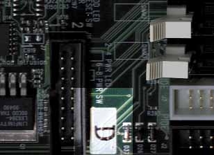
The Tyan Trinity 400 has been with us since the release of the 133A chipset and we have seen it grow through four revisions. The most recent revision, Revision 4 or Revision D (denoted by the D silk screened on the PCB), fixes some of the bugs in the previous version (Rev 3 or C) and removes the need for a jumper to select whether the Socket or Slot connector is in use.
Revision D
The Trinity 400 features both a Socket-370 and a Slot-1 connector, offering the end user a great amount of flexibility with CPU choices. Unfortunately, the way in which the board chooses the AGP clock ratio does not allow you to use a Socket-370 CPU with 133MHz FSB and have the board select a 1:2 AGP clock ratio.
You can read our Trinity 400 review for a more in-depth analysis of the board, but keep in mind that if you want to use a FC-PGA Pentium III on the Trinity 400, you need to have a board that is revision 3 (or C) or above. All previous revisions of the board only support Celeron CPUs in the Socket, but if you’re going to be using a Socket-370 to Slot-1 adapter then this warning does not apply to you.
The stability of the Trinity 400 was respectable, but not on par with what we’re used to from Tyan. The performance was just slightly behind that of the top performing Gigabyte GA-6VX-4X.
The Test
|
Test Configuration |
|
| Processor(s): |
Intel
Pentium III 733EB (for Slot-1 Motherboards)
Intel FC-PGA Pentium III 550E @ 733MHz (for Socket-370 Motherboards) |
| RAM: |
1
x 128MB Corsair PC133 SDRAM
|
| Hard Drive(s): |
Western Digital 153BA Ultra
ATA 66 7200 RPM
|
| Bus Master Drivers: |
VIA 4-in-1 v4.20 BMIDE Driver
|
| Video Card(s): |
NVIDIA
GeForce 256 SDR
|
| Video Drivers: |
NVIDIA
Detonator 3.76
VIA AGP GART 4.00 |
| Operation System(s): |
Windows
98 SE
|
| Motherboard Revisions: |
ABIT
VA6 Revision 0.5
AOpen MX64 Revision 1.0 ASUS P3V4X Revision 1.02 Elitegroup P6BAP-A+ Revision A Elitegroup P6BAP-Me Revision A Elitegroup P6VAP-Me Revision B EPoX K7XA Revision 0.3 FIC KA-11 Revision 2.2 Gigabyte GA-6VX-4X Revision 1.1 Gigabyte GA-6VX7-4X Revision 1.2 Shuttle AV64 Revision 1.3 Tyan Trinity 400 Revision D |
Performance
We noticed a huge variance in performance among the motherboards in this roundup. The range of performance figures could be due to a number of possibilities, but the most likely is a simple lack of attention to performance optimizations that could be easily accomplished by tweaking the BIOS. Dealing with the VIA chipsets is different than their Intel counterparts, and motherboard manufacturers need to learn how to deal with the intricacies of the chipsets. The performance figures you're about to see are indicative of a lack of attention to performance tweaking on the part of quite a few of the manufacturers.
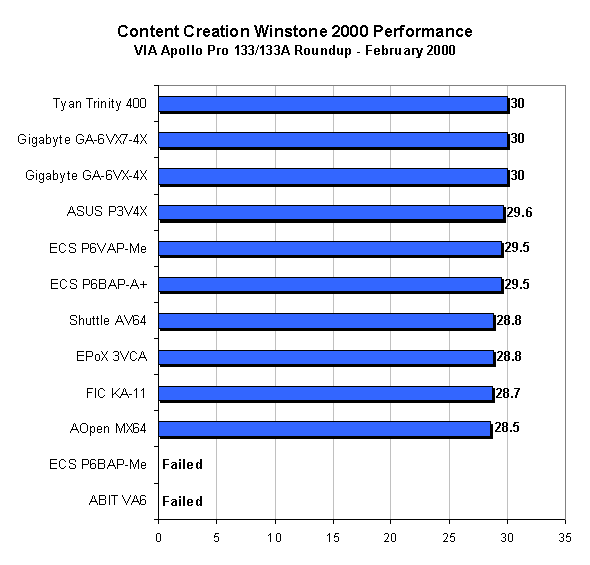
The performance of the boards that managed to complete the tests didn't vary much from one board to the next. This is what you'd expect from most motherboards, but as the following tests illustrated you sometimes have to expect the unexpected.
The ECS P6BAP-Me failed to complete our Winstone runs because it, being a Socket-370 only solution (thus requiring us to use a 550E known to be able to be overclocked to 733MHz) needed a boost in the core voltage in order to hit the higher clock speed (1.65v vs 1.60v). Unfortunately the board does not support the ability to tweak the core voltage of any CPU, which resulting in our 550E not being quite as stable as we'd like it to be at 733MHz and it definitely didn't help the system complete Winstone 2000.
The VA6 failed the test because of a problem with our VA6 board, we have mentioned this to ABIT but we have yet to see an updated revision from the company. There are many satisfied VA6 users out there but at the same time there are other users that have had similar experiences to ours with the VA6 where the board would not even complete a single test under Windows. We are still awaiting an updated revision of the motherboard from ABIT.
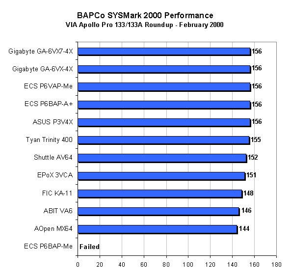
You begin to see a much larger performance range under SYSMark 2000 with the slowest board tested, the AOpen MX64 being a full 8% slower than the top five boards that tied for first place. While the AOpen is more stable than a few of the boards at the top, the Gigabyte boards are just as stable as the AOpen and perform at the top of the roundup. So it's not necessary to have a lower performing board in order to have a stable motherboard.
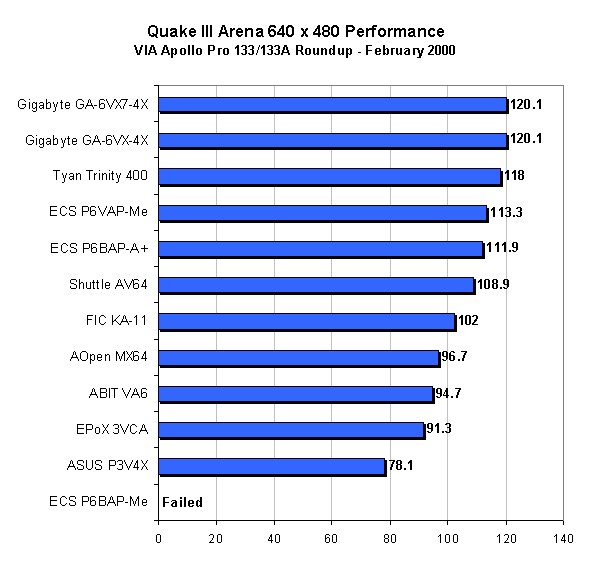
This is where we noticed the largest difference between motherboards. At the top of the list we have the two Gigabyte motherboards that score a full 42 fps than the slowest ASUS P3V4X in this test. The fact that there is such a large difference between motherboards in this test is inexcusable, motherboard manufacturers that performed below average here (if we consider the Shuttle AV64 to be average) need to seriously work on improving the performance of their Apollo Pro 133/133A implementations. Kudos to Gigabyte, Tyan, ECS and Shuttle for providing an example to follow.
Conclusion
 The
best overall motherboard in this roundup goes to Gigabyte for their GA-6VX-4X
which is the Slot-1 counterpart of their GA-6VX7-4X. While they both performed
similarly and were just as stable as one another, the 6VX-4X gets the Editor's
Choice award here because of the flexibility offered by the Slot-1 interface.
The 6VX7-4X offers no adjustable voltage settings, neither does the 6VX-4X,
but with the 6VX-4X you can use a Socket-370 to Slot-1 adapter with your FC-PGA
Pentium III and gain control over the voltage supplied to your CPU.
The
best overall motherboard in this roundup goes to Gigabyte for their GA-6VX-4X
which is the Slot-1 counterpart of their GA-6VX7-4X. While they both performed
similarly and were just as stable as one another, the 6VX-4X gets the Editor's
Choice award here because of the flexibility offered by the Slot-1 interface.
The 6VX7-4X offers no adjustable voltage settings, neither does the 6VX-4X,
but with the 6VX-4X you can use a Socket-370 to Slot-1 adapter with your FC-PGA
Pentium III and gain control over the voltage supplied to your CPU.
The ASUS P3V4X is another potentially powerful candidate for the Editor's Choice if ASUS could just improve the performance of the board. The issue seems to be related to a BIOS setting that isn't present in the setup of the P3V4X so it shouldn't be too difficult for ASUS to correct, only time will tell if ASUS takes care of this issue.
The performance issue is present with virtually all of the motherboards in this roundup, and it is a very disappointing scene. It has been just about two years since the last time we did a major motherboard comparison where there was a significant difference in performance among the entries. The VIA Apollo Pro 133/133A chipsets are viable alternatives, and although there are quite a few motherboard manufacturers out there that are using the solutions we're going to need a greater level of perfection from these manufacturers before the platform can get to the point the BX platform is today where you can go out and pick up virtually any board without having to worry about performance issues.
If motherboard manufacturers don't take it upon themselves to fix the problems with their boards, VIA needs to step forward and endorse only those manufacturers that properly implement their chipsets as well as follow a set of guidelines for performance and stability when using these chipsets. From the manufacturers that we've talked to, we've received the impression that VIA isn't nearly as cooperative as Intel with helping motherboard manufacturers with their designs. While this may be an illustration of the capabilities of a large company versus a smaller one, it is also a sign that VIA does need to do more if the problem's roots is indeed with them and not lax motherboard manufacturers.
Once again, kudos to the manufacturers such as Gigabyte, Tyan and Elitegroup that actually took the time to properly implement and tweak their Apollo Pro 133 and 133A boards. To the rest, we will be doing another roundup in a few weeks time, let's hope the picture changes by then.

