Original Link: https://www.anandtech.com/show/474
VIA Apollo KX133 Athlon Chipset - Part 1
by Anand Lal Shimpi on February 7, 2000 11:51 PM EST- Posted in
- CPUs
 The
slow demise of the Socket-7 platform quite possibly summed up a period in time
when the hardware enthusiast was given the most choices when putting together
a system. At the peak of the platform’s existence, there were three major CPU
manufacturers producing processors for Socket-7 motherboards, there were solutions
available in both AT and ATX form factors, and from a chipset standpoint, the
platform had three chipset solutions from Intel and another three from VIA.
That theme of variety from the old Socket-7 days has long since been abandoned; until well into the establishment of the Slot-1 platform, all chipsets manufactured were made by Intel. That same trend seemed to be mirrored with the introduction of AMD’s Athlon late last year. One of the worries for the success of the Athlon that we shared at AnandTech was platform chipset support. While AMD announced that both ALi and VIA would have solutions ready for the Athlon, as launch time approached, it quickly became obvious that neither the ALi or VIA solutions would be ready for the release of the Athlon.
So what chipset would the Athlon launch with? AMD had done all of their internal testing and tweaking using their own in-house developed chipset, internally known as the Irongate chipset but commonly known to us as the AMD 750 chipset. The AMD 750 boasted AGP 2X and PC100 SDRAM support courtesy of the AMD 751 North Bridge as well as Ultra ATA 66 courtesy of the AMD 756 South Bridge.
It wasn’t too long before Athlon based motherboards began shipping with hybrids of the AMD chipset and VIA’s upcoming solution. Motherboards like the ASUS K7M and FIC SD-11 featured AMD’s 751 North Bridge but VIA’s 686A South Bridge, in order to move away from using AMD as a chipset supplier.
Last November, we were told that VIA’s upcoming Athlon chipset, the Apollo KX133, was already complete and they were hard at work with motherboard manufacturers to make sure that the delicate implementation of the chipset was handled properly. This would help to eliminate any of the motherboard problems that the first wave of Athlon boards based on the AMD 750 chipset so regretfully boasted.
Finally, on January 10 of this year, VIA announced that they had begun volume shipping of the “first independently developed chipset to support the AMD Athlon processor” known to all of us as the KX133. The release of the KX133 puts VIA in the position of a great monopoly in the Athlon market since motherboard manufacturers will refrain from producing many (if any at all) AMD 750 based solutions and since ALi’s Athlon solution has yet to be seen other than behind a glass display case at last year’s Fall Comdex.
With the exception of a few Athlon motherboards that were being developed with the AMD 750 in mind, all Athlon motherboards that will be shipping from manufacturers that have yet to enter the Athlon motherboard market will be KX133 based solutions. It won’t be long before the AMD 750 disappears from the market and VIA assumes the role of exclusive Athlon chipset provider for the time being. Scary thought?
It shouldn’t be. VIA has never been known to abuse their power during the times when they have been given the upper hand in a market (i.e. Super7 market), the only question is, in spite of VIA’s history, can the KX133 step up to the plate and offer performance and compatibility (the latter being a weak point in VIA’s history) superior to that of the AMD 750?
The Chipset
The KX133 chipset actually isn’t very new. In fact, most of the technology that went into the design of the KX133 has been around for quite some time. Originally, the KX133 was supposed to be ready and shipping by the launch of the Athlon last August, but, unfortunately, according to VIA, that was delayed for a number of reasons, including the fact that they wanted to work closer with motherboard manufacturers on their implementations to get them right the first time.
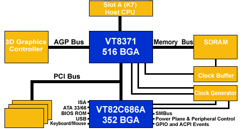
The KX133 itself takes advantage of a number of borrowed features from other VIA products. The chipset itself, in the usual VIA style, is divided into two parts, a 516-pin North Bridge, the VT8371, and a 352-pin South Bridge, the VT82C686A that we’re already quite familiar with.
VIA still hasn’t accepted an approach more like Intel’s Accelerated Hub Architecture, which, through the use of an all-purpose-bus, is capable of transferring data at 266MB/s. VIA’s KX133, like all previous VIA chipset, relies on the PCI bus to connect the North Bridge to the South Bridge thus offering a peak theoretical bandwidth figure of 133MB/s. This bottleneck, although still not very apparent with Athlon systems (the AMD 750 features the same “bottleneck” and performs just fine) is something that VIA will have to consider in future chipset implementations, they just chose not to start with the KX133.
VT82C686A South Bridge
We just mentioned that most of the KX133 design is “borrowed” from previous VIA chipsets, and the first example of that is the VT82C686A (commonly known as the 686A) South Bridge.
The 686A was first introduced on the Apollo Pro 133 chipset but is referred to as an option on the old Apollo Pro, a P6 chipset, as VIA’s Super South Bridge, this of course being an improvement over the 596B regular South Bridge. The 686A has been paired up with the 693 North Bridge for use with the Apollo Pro+, again with the 693A North Bridge for the Apollo Pro 133, and once again with the 694X North Bridge of the Apollo Pro 133A.
The flexibility of VIA’s North/South bridge setup is one reason they have kept it around for so long, and it has allowed them to use the 686A on their two Super7 chipsets, the MVP3 and the MVP4.
On the Athlon side of things, the 686A was the replacement South Bridge for the AMD 756 in designs that implemented the AMD 750 chipset. Now, the 686A is back once again with the Apollo KX133 chipset. As you can see, the 686A has been around for quite some time, and thus it didn’t take much effort for VIA to use it as the South Bridge of the KX133 chipset.
The 0.35-micron, 352-pin 686A remains unmodified from its original introduction and use on the P6 chipsets, and thus the specs remain the same. Let’s discuss the benefits of each one of these features to see what they actually accomplish:
· Inter-operable with VIA and other Host-to-PCI Bridges – As we just finished discussing, the fact of the matter is that the 686A can be used on a number of VIA chipset implementations, thus helping to keep costs down since VIA only has to manufacture one chip that can be implemented on a number of motherboard designs.
· Integrated PCI-to-ISA Bridge – This feature, present on the now old Intel piix4 and piix4e South Bridges but absent on the i820 and i810(E) chipsets, allows for the implementation of ISA slots on a motherboard that uses the 686A without having to use an external PCI-to-ISA Bridge. This helps save PCB space and cut costs. On the reverse side of things, ISA slots are quickly dying so this feature is becoming less of a necessity.
· Ultra ATA 33/66 PCI EIDE Controller – Just recently, Ultra ATA 33 has began to be saturated by the latest 7200 RPM IDE hard drives, so Ultra ATA 66 support is definitely a desired feature. While Intel is supposed to announce ATA-100 support in the near future, it will be a while before hard drives saturate the 66MB/s peak transfer rates of the Ultra ATA 66 specification.
· Integrated Super I/O Controller – Unique to the 686A, the integrated Super I/O controller takes care of all of the basic I/O needs of a motherboard. It provides the serial, IR, and parallel ports as well as the Floppy Disk Controller for the motherboard. Why is this so special? Well, currently no Intel chipset has these features integrated into any part of the chipset, meaning they have to resort to an external I/O controller to provide these functions. This external controller not only occupies PCB area on the motherboard it also adds the cost of another chip to the price of the motherboard. This is a feature the AMD 756 South Bridge does not support, one reason why many motherboard manufacturers chose to go with the 686A over the AMD 756 in their Athlon motherboard implementations.
· AC’97 & MC’97 Support – KX133 motherboards that take advantage of the Audio Codec ’97 support of the 686A South Bridge will feature an AC’97 controller placed on the motherboard that drives an integrated audio output while supporting the use of the AMR (Audio Modem Riser) slot for higher quality audio or modem support. The reason for the use of the AMR slot is to place the more sensitive components on an AMR slot so that motherboard manufacturers don’t have to increase the production time of their products because of the certification required for sensitive analog components such as those on modems or higher quality audio devices. This is also why, in spite of the presence of the AMR slot, the motherboard manufacturers will go ahead and include audio inputs/outputs on the motherboard itself, so they don’t have to worry about the certification time required by an AMR card in order to ship their boards to OEMs with integrated sound.
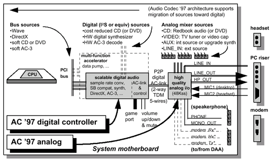
Remember that these AC’97 controllers depend on the host CPU to do most of the work associated with their particular tasks, but because of this they add a negligible amount to the final cost of the motherboard.
· Integrated Hardware Monitoring – Once again, by integrating hardware monitoring onto the 686A South Bridge, VIA helps to cut motherboard manufacturing costs by removing yet another chip from the PCB. Most motherboards use an external chip to provide hardware monitoring functionality which takes up PCB space and adds the cost of the chip to the motherboard. The integrated hardware monitoring can monitor 5 voltages (including the voltage supplied to the 686A chip itself), three temperatures (including the temp of the 686A) and two fans.
· Universal Serial Bus Controller – The 686A’s USB controller goes one step above Intel’s current USB implementation by allowing support for up to 4 USB devices.
In the end, the 686A South Bridges helps to integrate three commonly external chips (I/O Controller, Hardware Monitoring Controller, and South Bridge) into one chip. This helps to bring the cost of motherboards using the 686A down to costs lower than what the AMD 756 implementations placed them at. So far so good from VIA.
VT8371 North Bridge
 The
first “new” part of the KX133 is the 371 North Bridge, but even the 371 North
Bridge borrows some features and technology from VIA’s other flagship North
Bridge, the 694X. Let’s look at the 371’s features:
· High Performance Athlon CPU Interface – All this fancy statement means is that the 371 interfaces with the Slot-A connector on the motherboard using the Athlon’s EV6 bus. This interface is the “200MHz FSB” that most Athlon motherboard manufacturers throw around when it’s actually a 100MHz Double Data Rate FSB. This implementation remains relatively unchanged from the original AMD 751 North Bridge, meaning that the amount of available bandwidth has not changed (1.6GB/s).
· Fully Featured Accelerated Graphics Port (AGP) Controller – The 371’s integrated AGP controller is actually borrowed from VIA’s 694X AGP controller in that they both feature the same core. The controller features support for AGP 1X, 2X and 4X transfer rates, and because of its AGP 4X support, motherboard manufacturers can choose to implement an AGP Pro connector on motherboards based on the KX133 chipset. This is an improvement over the AGP 2X limitation of the AMD 751 North Bridge.
· Concurrent PCI Bus Controller – The integrated PCI controller is the same as the 694X’s (Apollo Pro 133A) PCI bus controller. It supports 5 PCI master devices, but motherboard manufacturers can implement more than 5 PCI slots, the added slots will simply be slave devices. Nothing special here.
· Advanced High-Performance DRAM Controller – The Memory subsystem of the KX133 is the biggest difference between the 371 North Bridge and the AMD 751 North Bridge. The 371 can address up to 8 RAS lines, meaning motherboard manufacturers can outfit their boards with up to 4 DIMM slots with support for double sided DIMMs in all of the slots.
The memory controller, once again, very closely resembles that on the 694X (Apollo Pro 133A), especially in the supported memory types. The 371 currently only supports PC133 and PC100 SDRAM (no DDR SDRAM support) as well as VC133 and VC100 Virtual Channel SDRAM support.
The memory bus can operate (officially) at either 100MHz or 133MHz, this is an improvement over the sole 100MHz setting present on motherboards based on the AMD 750 chipset. Keep in mind that we’re talking about the memory bus frequency, not the front side bus frequency, the latter which operates at 100MHz DDR regardless of the frequency of the memory bus. The 133MHz memory bus frequency allows the KX133 to attain an available 1.06GB/s of peak memory bandwidth, up from the 800MB/s on the AMD 750. This is the biggest improvement the KX133 offers over the AMD 750.
The chipset itself supports up to 2GB of memory, but it’s up to the motherboard manufacturers to make sure that their boards can reach this capacity properly without sacrificing stability.
Because most of the 371 chip itself is borrowed from the 694X (with the obvious exception of the interface to the EV6 bus), functions such as AGP 4X and the 133MHz memory bus frequency shouldn’t have any related problems since we’ve already seen them in action on Apollo Pro 133A boards.
Memory Bandwidth – PC133 isn’t Enough
While it is true that the 1.06GB/s of available peak memory bandwidth provided for by the PC133 support of the KX133 is a great improvement (33% to be exact) over the 800MB/s provided for by the PC100 support of AMD’s 750 chipset, it still isn’t enough.
With AGP 4X capable of transferring up to 1.06GB/s of data to/from system memory and the peak available memory bandwidth equal to that number, factoring in memory bandwidth required by the CPU and other parts of the system, PC133 support isn’t enough.
The true answer to this problem lies in Double Data Rate SDRAM, or DDR SDRAM for short. As we know from previous articles, DDR SDRAM works much like the AGP bus and the Athlon’s EV6 bus by transferring data on both the rising and falling edges of the clock. By doing this, a 100MHz DDR SDRAM module can actually do twice as much work per clock cycle, offering a peak bandwidth figure equal to that of a regular 200MHz module.
From a pricing standpoint, DDR SDRAM costs barely 3 – 5% more than regular SDRAM. The only thing the market is waiting for is availability of DDR SDRAM chips. We have already seen them used on some graphics accelerators based on NVIDIA’s GeForce processor, it won’t be long until we see them used on desktops. Unfortunately, since DDR SDRAM requires additional signaling pins to interface with the memory controller, the 371 North Bridge and all KX133 motherboards that support regular SDRAM won’t support DDR SDRAM.

A DDR SDRAM Module
When will a DDR version of the KX133 be available? According to VIA, their first DDR chipset will be for the P6 bus, meaning that Pentium III owners will get a shot at DDR SDRAM before Athlon owners will. It won’t be until after the introduction of VIA’s DDR P6 chipset that we will see the introduction of the DDR version of the KX133.
Micron’s Samurai chipset (P6 bus) already supports DDR SDRAM, and VIA will most likely be licensing the technology behind the Samurai for use in their workstation class DDR chipset (P6 bus). We haven’t heard any mention of an equivalent chipset for use with the Athlon, but porting the DDR memory controller to the KX133 shouldn’t be too difficult once they get a working chipset in production.
Chances are that we’ll see AMD’s 760 chipset with DDR SDRAM support before VIA’s DDR version of the KX133 hits the streets.
Virtual Channel SDRAM – Where are you?
Originally covered in our review of VIA’s Apollo Pro 133A chipset, NEC’s Virtual Channel SDRAM is a work around for the memory bandwidth limitations of PC133 SDRAM in an AGP 4X compliant system.
It works like this: Virtual Channel Memory uses a set of high speed static registers (high speed memory) between the memory core and I/O pins (between the memory itself and its connection to the "outside world" or memory masters). These high speed registers provide each memory master (anything that accesses system memory) with its own "Virtual Channel" to the SDRAM. This helps reduce latency and increase the efficiency of the amount of bandwidth available to your system as a whole. This concept is better described by the diagram below:
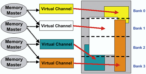
Specifically, VC-SDRAM features 16 virtual channels, each 128 bytes in width. The 16 channels are split evenly among the two internal banks each VC-SDRAM module features.
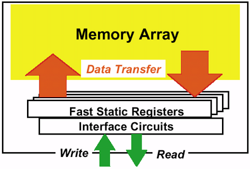
Unlike DDR-SDRAM, VC-SDRAM does not increase memory bandwidth by a fixed amount but it frees up bandwidth for use as a result of greater memory bus efficiency. NEC claims a figure of up to 90% efficiency, but that depends entirely on the number of memory masters accessing memory and the nature of each access.
At the same time, VC-SDRAM does not decrease latency by a fixed amount; rather, it depends on the nature of the accesses it decreases the latency for simultaneous accesses by multiple memory masters.
While the KX133’s North Bridge does support VC-SDRAM, finding Virtual Channel SDRAM can be a bit tricky. Other than a few modules that have been floating around (two of which we were lucky enough to grab), VC-SDRAM is a general rarity in the market. After a bit of researching, all we could find out is that all of the VC-SDRAM chips being produced by NEC are being purchased by an unnamed OEM, and it isn’t even clear whether this OEM is using the chips for use on memory modules or for some other purpose.
Regardless, if you want to get your hands on VC-SDRAM, don’t waste your time. It doesn’t seem like it’s a viable option, especially since, if you ever decide to move to a chipset that does not support VC-SDRAM, your modules are not re-usable. While they work in regular 168-pin SDRAM slots, they won’t work unless the memory controller on the chipset specifically supports VC-SDRAM. That support is currently limited to three VIA chipsets: the Apollo Pro 133, the Apollo Pro 133A and the KX133.
AMD 750’s SuperBypass
One redeeming feature about the AMD 750 chipset, at least on paper (since we have yet to delve into real world performance numbers) is something present in the latest revisions of the AMD 751 North Bridge, called SuperBypass.
The feature, originally discovered by former AMD employee Silvino Orozco of Tom’s Hardware Guide, apparently helps to reduce memory latencies in the AMD 750 chipset.
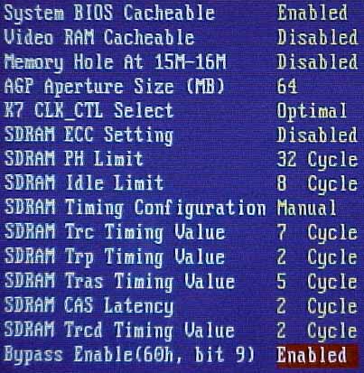
The SuperBypass feature was intended to be enabled on all AMD 750 chipsets from the start, but, unfortunately, it wasn’t implemented properly in earlier versions of the chipset. The latest revisions of the chipset do feature support for the setting and if your chipset supports it then it should be automatically enabled by default.
On Gigabyte’s internal BIOS releases for their AMD 750 based GA-7IX, there is a setting under Chipset Features entitled ‘Bypass Enable(60h, bit 9)’. This setting isn’t present in the production BIOS, but enabling it on a motherboard without SuperBypass support did not result in the feature being turned on. If your chipset properly supports the feature then the latest BIOS update should leave it enabled by default.
Enabling SuperBypass can result in a fairly noticeable performance increase. Unfortunately, because not all revisions of the chipset support it, it’s not a feature that you can guarantee will be enabled on all AMD 750 motherboards.
The Reference Design
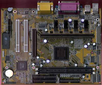
VIA supplied us with one of their reference designs used by motherboard manufacturers as a guideline on how to properly implement the KX133 chipset. The board they supplied us with is their microATX reference board. This board isn’t publicly available, but don’t be surprised if you see other microATX KX133 motherboards popping up that look a lot like it.
The board is a four layer design which, upon finding it out, immediately triggered a light bulb over our heads in the lab. One of the biggest drawbacks of AMD’s Fester reference design with the 750 chipset was that it was a 6-layer motherboard. While 6-layer PCBs are generally better than 4-layer PCBs because they allow for greater insulation between the power and ground traces, they are also considerably more expensive. This was one of the reasons that companies like ABIT, who won’t manufacture a 6-layer motherboard for reasons of maintaining set profit margins (which are quite low in the motherboard industry), never made an Athlon motherboard. While it isn’t the only reason, you can expect many more motherboard manufacturers to come out with KX133 designs than they did with AMD 750 based designs simply because they can make 4-layer boards.
The 4-layer reference design does hold one key advantage for KX133 motherboards as a whole - they should be noticeably cheaper than their AMD 750 counterparts. Coupled with the highly integrated 686A South Bridge, KX133 solutions should be quite affordable. With a microATX reference design, you can expect to see some pretty cheap microATX KX133 boards pop up every now and then for use with AMD’s upcoming Spitfire chip, a low-cost Athlon with on-die L2 cache.
VIA does have a standard ATX reference board; we managed to take a look at one of those back at Fall Comdex ’99. The most noticeable feature of that reference design was that the board itself was quite large, much like the FIC SD-11. It is highly doubtful that many manufacturers will be following that design down to the last point simply because of the incredible size of the board, but don’t worry, not all KX133 boards will be microATX solutions.
The reference board did not provide us with any stability problems, but that doesn’t mean anything for the shipping KX133 solutions. As long as motherboard manufacturers follow VIA’s guidelines and their reference designs closely, KX133 motherboards shouldn’t have any problems, but as soon as they start cutting corners to save costs, this could change.
Right now, the physical hardware implementation of the KX133 chipset is complete on most motherboards that are scheduled to ship before the end of this quarter. Now, the main hurdle that has to be overcome is tweaking the BIOS for optimal performance and stability.
Unfortunately, most of the KX133 boards that were supposed to be ready by January have been delayed. AOpen’s KX133 solution has been delayed until late February or early March, and Tyan’s solution is still a few weeks away. EPoX will have one of the first shipping KX133 based solutions world-wide, and we will be taking a look at their solution shortly.
The EPoX design is done, the hardware is complete and the shipping revision of the motherboard is ready. The BIOS is the only limitation as they’re still working towards tweaking the BIOS to ensure maximum performance and stability.
Unlike the first Athlon boards based on the AMD 750 chipset, there will be quite a few KX133 based solutions on the market. This should anger Intel quite a bit since the one manufacturer they object to being on a motherboard more than AMD is VIA. VIA chipsets are in direct competition with Intel’s solutions (whereas AMD’s 750 wasn’t “directly” competing with Intel’s chipsets) and thus Intel will be using every trick in the book to try and get them out of the picture (including trying to stop VIA from exporting products to the US).
The Test
|
Windows 98 SE Test System |
||||
|
Hardware |
||||
|
CPU(s) |
AMD Athlon 800 |
|||
| Motherboard(s) |
VIA
KX133 Reference Board
|
Gigabyte GA-7IX | ||
| Memory |
128MB PC133 Corsair SDRAM |
128MB
VC133 NEC VC-SDRAM
|
128MB
PC100 Corsair SDRAM
|
|
| Hard Drive |
IBM Deskstar DPTA-372050 20.5GB 7200 RPM Ultra ATA 66 using VIA BMIDE Drivers |
|||
| CDROM |
Phillips 48X |
|||
| Video Card(s) |
NVIDIA GeForce 256 |
|||
| Ethernet |
Linksys LNE100TX 100Mbit PCI Ethernet Adapter |
|||
|
Software |
||||
|
Operating System |
Windows 98 SE |
|||
| Video Drivers |
|
|||
|
Benchmarking Applications |
||||
| Gaming |
GT
Interactive Unreal Tournament 4.04 UTbench.dem |
|||
| Productivity |
BAPCo SYSMark 2000
Ziff Davis Content Creation Winstone 2000 Intel Performance Measurement Utility |
|||
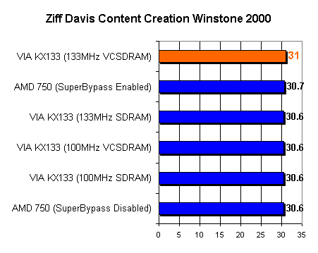
There isn’t much of a performance difference in Content Creation Winstone 2000 simply because most of the applications fit within the Athlon’s 128KB L1 cache and/or its 512KB L2 cache.
Any difference in performance here is negligible since the range of 0.4 Winstone points isn’t enough to justify any performance analysis.
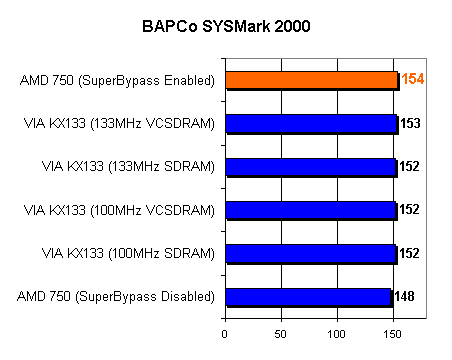
While the performance improvement the KX133 with regular SDRAM offers over the AMD 750 chipset solely because of the 133MHz memory bus is barely 3%, turning on SuperBypass, a feature exclusive to the AMD 750 chipset that helps to reduce memory latencies, the AMD 750 jumps ahead of even the KX133 using 133MHz Virtual Channel SDRAM.
VIA has been notorious for having memory timing issues with their integrated DRAM controllers, the most recent case being the 694X (Apollo Pro 133A) whose memory performance is noticeably slower than that of an equivalently clocked BX setup.
Since the KX133’s North Bridge borrows the DRAM controller from the 694X you would expect the same timing issues to transfer over to the KX133, and they do. The AMD 750 with SuperBypass enabled, even while running its memory bus at 100MHz, seems to be ever so slightly faster than the KX133 with a 133MHz memory bus, at least in business and content creation applications.
This is a tad disappointing. However, in order to investigate the memory performance of the KX133’s DRAM controller, we dug into our stacks of benchmarking software and pulled out two rarely used CDs: Intel’s Business and Consumer Application Launcher software.
For those of you that don’t remember, Intel’s Business and Consumer Application Launcher benchmarks were supplied to us by Intel in order to show off the SSE performance of the Pentium III as well as to show off the memory performance of RDRAM and the 133MHz FSB. While it was a horrible set of benchmarks to compare non-Intel processors to Intel processors that featured the SSE instructions, it is a wonderful way to compare memory performance.
The Business Application launcher features 3 applications, Naturally Speaking Professional (voice recognition software), Netshow Encoder (AV encoding software), and Photoshop 5.0 (digital imaging software). The Consumer Application launcher features 2 applications, PhotoDeluxe Home Edition (consumer level digital image editing software) and AVID Cinema (consumer level digital video editing software). The descriptions of the tests are listed below:
Intel Performance Measurement Utility - Business Application Launcher 1.2
NATURALLYSPEAKING
PROFESSIONAL v3.52
DRAGON SYSTEMS, INC.
--------------------
Dragon NaturallySpeaking v3.52 is a continuous speech recognition application
that converts speech into text. The script in the performance measurement utility
CD plays a pre-recorded wave file (a recorded speech) using Dragon's PlayWave
utility. The utility feeds this wave file into NaturallySpeaking which then
converts the wave file to text. The time taken to load application and wave
file and complete the conversion is used as the performance metric.
The speech recognition program created by Dragon Systems is composed of several
pieces including the underlying engine, the user interface, and several middle
layers with language models, rules, and acoustic models.
NETSHOW ENCODER 3.0
MICROSOFT CORPORATION
---------------------
Using mpg4c32 DLL v3.0.0.3433, dated 02/08/99
Netshow Encoder encodes audio and video content into an Advanced Streaming Format
(ASF) stream. The content can be from a live source or an existing .avi, .wav,
or .mp3 file. The output from Netshow Encoder is a stream of information that
can be heard or viewed with Microsoft Windows Media Player, or sent to a Netshow
server for multicasting, unicasting, or storage. The performance measurement
utility is testing the MPEG-4 Video Codec which is embodied in the mpg4c32 DLL.
The input file is a 30 second 320x240 AVI clip from an Intel MMX(TM) technology
advertisement. The script encodes this file using the MPEG-4 Video Codec. The
time taken to load the application and input file and complete the encoding
is used as a performance metric.
PHOTOSHOP 5.0
ADOBE SYSTEMS, INC.
-------------------
Using plug-ins MMXcore.8bx (v5.0.3), LightingEffects.8bf (v5.0.4) and
Wind.8bf (v5.0.4).
Adobe Photoshop 5.0 is an application which provides tools for digital image
enhancement, photo retouching, and image compositing, and is typically used
by graphic designers, photographers, and electronic publishers. The script loads
Photoshop, applies the same sequence of operations to two different image files
(boat.tif and Temple8.tif, which are located under the scr_data directory on
the CD), and then quits the application. The sequence of the operations is:
1) Load the image file, resize the image to a width of 2048 pixels (the height is adjusted automatically based on the aspect ratio of the original image), and zoom it two times to 33.3% of its original size.
2) Apply the Unsharp mask with an amount of 50, radius of 1 pixel and a threshold of 0. Then apply the Sharpen Edges filter, change the CMYK color setting to ICC mode, and add Parallel directional lighting effect with no texture.
3) Use Sharpen More filter. Add uniformly distributed noise with an amount of 9. Apply parallel directional lighting effect with no texture. Use the Unsharp mask with an amount of 50, radius of 1 pixel and a threshold of 0.
4) Apply Maximum filter
with a radius of 1 pixel. Resize the image to 1536 pixel wide (the height is
adjusted to keep the original aspect ratio). Change the color from RGB to CMYK.
Add stagger wind effect from the right. The time to load the application and
image files and complete the operations is used as the performance metric. Note
that not all of the Photoshop files and plug-ins are included on the performance
measurement utility CD, as not all were needed to run the script. In a
test where the full application was loaded, the typical speed up seen on a Pentium
III processor was 29% compared to a Pentium II processor at the same frequency.
Results seen here may be marginally faster due to a slightly shorter application
load time.
Intel Performance Measurement Utility - Consumer Application Launcher 1.0
PHOTODELUXE HOME
EDITION 3.1
ADOBE SYSTEMS, INC.
-------------------
Using MMXcore.8bx (1/29/99) and Lighting.8bf (1/13/99) plug-ins
Adobe PhotoDeluxe Home Edition is an application which provides tools for digital
enhancement, along with extensive content to create photo-filled projects. This
product is typically used by digital hobbyists and families. The performance
measurement utility applies various filter sequences to three images (Roses.jpg,
Boyclimb.jpg and Seattle.bmp) that can be found in the scr_data directory on
the CD.
The script consists of these
3 phases:
1) Load the Rose.jpg file. Zoom in once to view the picture at 50%. Apply Sharpen
Edges and Facet filter. Continue with Pinch Distortion of value 65. Spherize
the image with 75 as the amount and normal mode. Add Ripple with 100 as the
amount and medium size. Add Lighting Effects with Spotlight style, 35 as Brightness
and 69 as the spotlight size. Add Stagger Wind effect from the right. Find Edges
for the picture. Apply instant fix. Apply right and vertical Orientations. Set
the photo width to 419. Close
the file without saving.
2) Load the Boyclimb.jpg file. Zoom In once to set picture size at 33.3%. Apply Twirl at 50 degree angle. Add Pinch distortion with value 65. Stylize with Stagger Wind from the right. Apply Rectangular to Polar Funnel distortion. Motion Blur at 0 degrees. Add Lighting Effects with Spotlight style, 35 as Brightness and 69 as the spotlight size. Exercise Right and vertical Orientations. Adjust photo width to 600. Close the file without saving.
3) Load the Seattle.bmp
file. Zoom in once to set picture size at 50%. Sharpen the picture. Remove dust
and scratches from the picture. Unsharpen the picture. Apply Blur_More. Apply
Twirl at 50 degrees and Spherize the image with value 75 in normal mode. Stylize
with Stagger Wind from the right. Add Lighting Effects with Spotlight style,
35 as Brightness and 69 as the spotlight size. Apply Despeckle and dust noises.
Close the file without saving.
The time to load the application and image files and complete the operations
is used as the performance metric. Note that not all of the PhotoDeluxe files
and plug-ins are included on the performance measurement utility CD, as not
all were needed to run the script. In a test where the full application was
loaded, the typical speed-up seen on a Pentium III processor was 68% compared
to a Pentium II processor at the same frequency. Results seen here may be marginally
faster due to a slightly shorter application
load time.
AVID CINEMA
AVID TECHNOLOGY, INC.
---------------------
Using Ligos MPEG-1 plug-in v1.0.03
Avid Cinema is a video editing tool that is used to create new movies or add
impact to existing videos by using editing techniques, music, voice-overs, titles
and special effects.
The performance measurement
utility loads Avid Cinema and opens a file called Surfer.cma which is located
in the \Scr_data\Avidcnma directory. The file has 5 clips of wind surfers (Beach
Scene.mov, Jump.mov, Radical.mov, The Big One.mov and Zoom Out.mov) which total
23 MB. Go to the Finish Movie mode and export the file to an MPEG-1 file using
the Ligos MPEG plug-in for Avid Cinema by selecting the Ligos MPEG-1 format.
Save the file and exit the application. The saved MPEG file has a size
of 5.6 MB.
The time to load the application and image files and complete the operations
is used as the performance metric.
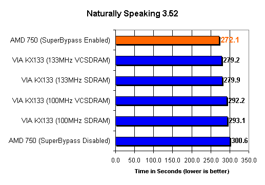
The Naturally Speaking tests focus heavily on memory transfers which is why you can see the fairly large performance range. As we would expect, at the bottom of the list we have the regular AMD 750 chipset with its 100MHz memory bus.
Virtual Channel SDRAM does seem to have some positive effect here as using it on the KX133 does improve performance slightly over using regular SDRAM. However, the performance difference is well under 1% so once again, there is no real reason to go crazy if you can’t find VC SDRAM to use with your new system.
The move to the 133MHz memory bus does seem to help out quite a bit here, as we would expect it to because of the memory bandwidth dependent nature of the Naturally Speaking test (it converts an audio file to text on the fly).
The most surprising result is that with SuperBypass Enabled, the AMD 750 even with its 100MHz memory bus is actually faster than the KX133 using 133MHz Virtual Channel SDRAM. Here we have another example of VIA’s memory timing issues that have haunted them in the past. Luckily for VIA, the performance difference between the AMD 750 with SuperBypass enabled and the KX133 isn’t too great.
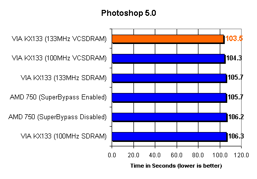
The Photoshop test is also quite memory bandwidth dependent and because of that dependency we have the Virtual Channel SDRAM scores taking over the top two spots. The efficiency of VC-SDRAM helps to boost the scores here, and, although it is not by an enormous amount, it is enough to give the 100MHz VC-SDRAM a slight lead over the 133MHz SDRAM.
With SuperBypass enabled, the AMD 750 with 100MHz SDRAM is as fast as the KX133 with 133MHz SDRAM. Only when using the currently unavailable Virtual Channel SDRAM can the KX133 jump ahead of the AMD750, but even then by only a small amount.
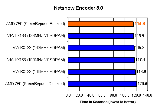
Once again, we have the AMD 750, with SuperBypass enabled, at the top of the charts, just slightly ahead of the KX133 using 133MHz VC-SDRAM.
The Virtual Channel memory doesn’t do all that much here because the Netshow Encoder test is much like the Naturally Speaking test where the efficient usage of available memory bandwidth isn’t key to obtaining higher performance because of the lack of enough memory masters accessing the system memory.
With SuperBypass disabled however, the added memory latencies push the AMD 750 slightly behind that of the KX133 with 100MHz SDRAM.
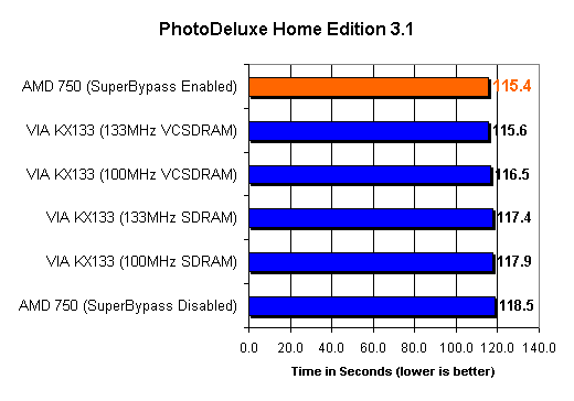
The PhotoDeluxe test resembles the previous tests in that the AMD 750 chipset with SuperBypass enabled comes out on top.
The slower memory performance of the KX133’s memory controller keeps the KX133 scores below that initial AMD 750 mark, and the use of VC-SDRAM does help performance a bit but not tremendously.
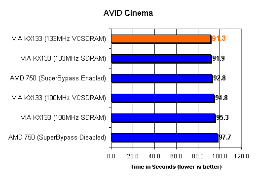
The AMD 750 with SuperBypass disabled comes in last place in this test, but when the feature is enabled the performance of the system jumps up to almost on par with the KX133 using 133MHz SDRAM.
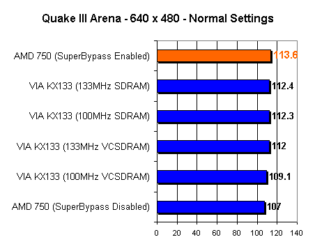
With SuperBypass enabled, the AMD 750 chipset jumps to the top here, in spite of its 100MHz memory bus. Simply disabling SuperBypass (or using a chipset revision without support for the feature) causes a 6% performance drop and quickly puts the 750 at the bottom of the chart.
The slow gaming performance is classic of VIA chipsets and has been carried over from the 694X which doesn’t perform as well as the Intel BX chipset under gaming situations on a clock for clock basis.
An even more interesting thing to point out is that the use of VC-SDRAM doesn’t help performance here at all, it actually hurts it. This could be due to VIA’s VC-SDRAM implementation or possibly timing issues related to using VC-SDRAM on the reference motherboard.
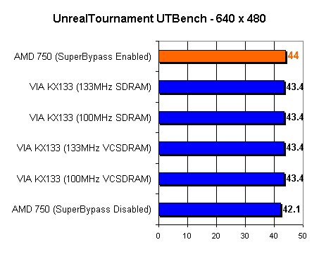
Here, the performance range isn’t very noticeable. Because of limitations in the Unreal engine, the 133MHz memory bus doesn’t do anything for performance here. The only clear outliers are the AMD 750 with SuperBypass enabled and disabled, which take the lead and bring up the rear respectively.
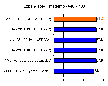
Expendable, a very memory bandwidth dependent game, illustrates a noticeably difference only between the AMD 750 with SuperBypass disabled and the rest of the setups. The KX133 using 133MHz VC-SDRAM pulls slightly ahead of the KX133 with regular PC133 SDRAM because of the increased efficiency of memory bandwidth utilization with VC-SDRAM, but the performance difference is barely noticeable at best.
Conclusion
Now that the highly anticipated KX133 is here, there are a number of things that must be said before you can simply base a conclusion on the performance figures mentioned in our tests.
First of all, finding motherboards based on the AMD 750 chipset will become increasingly difficult as the KX133 motherboard solutions become available on the market. This should happen within the next two months, although you’ll be able to buy KX133 motherboards within a few weeks.
Secondly, although the AMD 750 with SuperBypass enabled is on-par with, and sometimes faster than the KX133 even when using a 133MHz memory bus, keep in mind that not all revisions of the AMD 750 chipset support this feature. So while the AMD 750 may be the faster overall chipset, keep in mind that not all revisions of the chipset are created equal.
Third, the KX133 may be slower than the AMD 750 with SuperBypass enabled, but things could be much worse. For one thing, we noticed no AGP incompatibility problems with AGP 4X video cards and the KX133 chipset (AGP 4X was enabled for our test GeForce card using the Detonator 3.68 drivers) which was received by a huge sigh of relief after expecting quite a few AGP related problems from this chipset (judging by past history).
The performance of the KX133 isn’t noticeably slower than the AMD 750 either, and for a user looking to build a new Athlon system, going with the KX133 chipset will open them up to a variety of motherboards that wouldn’t be options if they were opting for a board based on the AMD 750 chipset. The true test will have to be when other manufacturers begin shipping their KX133 boards. It will be interesting to see if, with a few BIOS tweaks, the performance of the KX133 can be improved.
The AGP 4X support of the KX133 isn’t a big deal, it’s mainly a marketing ploy. From our tests, the difference between AGP 4X and AGP 2X is negligible. The biggest performance benefit of the KX133 is its PC133 SDRAM support which can come in handy for applications that are very dependent on memory transfers (such as professional level applications, image editing software, voice recognition, etc…).
The Virtual Channel SDRAM support of the KX133 looks very interesting on paper, but in reality it means nothing. The relative unavailability of VC-SDRAM modules to anyone but this mysterious OEM that seems to be purchasing all of the chips is a big downside. Secondly, the performance advantage, or lack thereof, that VC-SDRAM holds over regular SDRAM isn’t worth the trouble to go searching for it.
The biggest selling point for the KX133 will be its cost. Because of the highly integrated 686A south bridge and the 4-layer PCB design of the KX133 reference boards, motherboards based on the KX133 chipset should be noticeably lower priced than those based on the AMD 750. It is because of its cost that the KX133 chipset gets our recommendation, not because of its AGP 4X support or VC-SDRAM support, but because of the bottom line: its pricetag.
If you’re going to be building an Athlon system in the next few weeks you’ll probably want to go for a KX133 based motherboard. If you can wait, then in a few months AMD should have their own DDR chipset for the Athlon that will assume the place of the KX133 as the chipset to have and it should offer a nice performance premium over the KX133 and the AMD 750.
On the topic of dual processor Athlon chipsets, VIA will not be producing one in the foreseeable future leaving AMD as the only option for a dual processor Athlon chipset.
In the end, is it really all that odd that CPU manufacturers seem to know how to make chipsets that allow their CPU to perform optimally?

