
Original Link: https://www.anandtech.com/show/400
Intel Pentium III E FC-PGA (Socket-370)
by Anand Lal Shimpi on October 26, 1999 11:22 PM EST- Posted in
- CPUs
When Intel released the Slot-1 Pentium II in 1997, the market marveled at its size and criticized Intel for taking a step in the wrong direction. While the rest of the CPU market was happily resting on the Socket-7 platform, Intel was pushing their customers towards a $1000 chip that could fit into no socket known to man.
From Intel’s perspective, the move was necessary. The presence of the L2 cache on the motherboard was a bottleneck that the market knew well; unfortunately, no viable solution to the problem was at hand, so things continued the way they had been.
Intel’s first attempt at removing the bottleneck was to place the L2 cache in a package alongside the CPU that operated at the speed of the CPU. Keep in mind that this did not mean placing the L2 cache on the same die as the CPU, rather placing it near the die in a completely separate package. The name of this creation was the Pentium Pro.
At its peak, the Pentium Pro was manufactured on a 0.35-micron process that simply did not allow for a full 256KB, 512KB, or 1MB L2 cache on its die. So the package was separate from the core, but before the processor could be tested and put through Intel’s rigorous quality control tests, the two packages had to be joined and thus a full processor produced. There was no way of testing the CPU independently from the L2 cache, so if there was a problem in either of the two packages, the entire CPU had to be thrown away.
The second attempt was made in 1997, as we said earlier, with the release of the Pentium II, the first Intel CPU to make use of a Single Edge Contact Connector (SECC) or Slot-1 interface. The SECC card featured 512KB of L2 cache on the card itself, which could be manufactured by any outside source and still allowed the CPU to be tested prior to assembly. This card solved some of the problems posed by the Pentium Pro, but it also created new problems, such as those associated with the card that the actual Pentium II CPU was mounted on. The idea of placing the L2 cache on the die of the processor was still not within Intel’s reach. However, it did fall within their reach the following year, with the release of the Celeron A processor.
At what can be arguably considered to be the peak of Intel’s 0.25-micron production, the Celeron A was the first Intel CPU to feature L2 cache on the processor’s die itself. This means that the L2 cache is a physical part of the processor’s core and not contained within a separate package. The Celeron became the first desktop Intel processor since the Pentium II that had no use for the SECC processor card it was placed on. We were told that we wouldn’t see the next CPU that fit this description until Intel made the move to 0.18-micron.
The 0.18-micron fabrication process is finally upon us. The smaller fabrication process means that CPUs get faster, prices get lower and chips get tinier. The latter is the point that we address today, as we take a look at Intel’s Flip Chip PGA Pentium III E. The term Flip Chip is just a term that describes the Socket-370 version of the Organic Land Grid Array (OLGA) core that allows the heatsink to be attached directly to the die.
As we know from our review of the Pentium III E, otherwise known as the Coppermine processor, the ~29 million transistor CPU is the first desktop processor from Intel manufactured on the 0.18-micron process. The die features a full 256KB of L2 cache which makes the SECC-2 processor card a waste of space and more importantly, a waste of money. Since Intel already has a socketed platform ready (Socket-370, used by the Celeron CPUs), it would make perfect sense for Intel to make the transition to a socketed platform for their new Pentium III E. And thus we have the creation of the Socket-370 Pentium III E processor, or officially, the FC-PGA Pentium III E.
The Chip
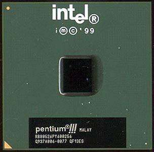 The FC-PGA Pentium III E (from hereon
referred to as the FC-PGA) is intended to be a contender in the high performance lower
cost market. The reason for the inclusion in the lower cost market as
opposed to the low-cost market is because the FC-PGA is not Intel’s low-cost chip;
that’s still the Celeron. Instead, the FC-PGA is a more affordable Pentium III E
(courtesy of its socketed design) that is only available at lower clock speeds in order to
encourage users that want the added speed to go after the more expensive Slot-1 Pentium
III E CPUs.
Eventually, Intel will ramp up the production of FC-PGA parts and virtually replace the SECC-2 parts in Intel’s production line by the end of 2000 although by the end of 2000 the FC-PGA parts will most likely be on a different socket platform (not Socket-370).
The current FC-PGA parts are available in two clock speed flavors, 500MHz and 550MHz, both running off of the 100MHz FSB. Both of these CPUs operate at a 1.60v core voltage as opposed to the 1.65v core of their Slot-1 counterparts, and both of them are Socket-370 compatible.
The term "Socket-370 compatible" does not mean that the FC-PGA will work in all Socket-370 motherboards, it just means that it is compatible with the Socket-370 interface (they will plug into a Socket-370 socket). The requirements a motherboard must meet in order for the FC-PGA to operate properly are as follows: the board must feature a Socket-370 interface, the board must support the 1.60v core voltage and finally, and most importantly, the board must also support the VRM 8.4 DC-DC Converter Guidelines. While most Socket-370 motherboards that are out on the market today meet the first two requirements, it is the third that will keep the FC-PGA out of most of our systems.
With every processor release, Intel also releases a set of guidelines that motherboard manufacturers should follow so that their products will be compatible with the new processor. Part of these guidelines are the design specifications that address what voltage regulator module (VRM) implementation needs to be placed on the motherboard. When the Pentium II was released, motherboard manufacturers had to follow the VRM 8.1 guidelines and upon the release of the Celeron processor the VRM 8.2 specification had to be adhered to. Intel’s higher end CPUs and multiprocessor systems also require a different VRM specification -- VRM 8.3 for all Xeon motherboards and optional for dual processor Slot-1 Motherboards. How does this apply to the FC-PGA running in older motherboards?
Each VRM specification is generally backwards compatible as long as it applies to CPUs of a similar family. For example, a motherboard with a VRM that meets the 8.2 guidelines will have no problem suiting an original Pentium II CPU that required the 8.1 specification. Obviously, this compatibility doesn’t work both ways (Intel can’t predict the voltage requirements of future processors) and thus a Pentium III CPU won’t work in a motherboard that only meets the VRM 8.1 specification. Make sense? Well, guess what the FC-PGA requires? Compliance with the latest VRM 8.4 guidelines, which currently, no Socket-370 BX motherboard officially supports. This means that all the users that picked up ABIT’s BP6 with hopes of upgrading to dual Pentium III E processors are out of luck.
We also tried the FC-PGA in our Apollo Pro 133A based Tyan S1894 motherboard, to no avail as well; it seems as if even the latest motherboards do not support the VRM 8.4 specification.
The FC-PGA has not changed the Socket-370 Voltage Identification Definition (VID) pinout that was originally defined with the Celeron. This means that the VID pins on the FC-PGA correspond to the same settings on the Socket-370 Celeron. If this weren’t the case, then older Celeron CPUs wouldn’t be able to work on newer Socket-370 motherboards that are FC-PGA compatible.
So where CAN we use the new FC-PGA?
We’re just going to have to accept the fact that our beloved Socket-370 motherboards do not support the new FC-PGA. This does not mean that future Socket-370 motherboards won’t support it. Currently, all i810E motherboards support the FC-PGA and are in full compliance with the VRM 8.4 guidelines. For those of you not familiar with the chipset, the i810E is the successor to the i810, adding support for the 133MHz FSB and an optional 133MHz Display Cache. The i810E features Intel’s integrated i752 graphics processor, which is no where near a good gaming solution by today’s standards, scaring many potential FC-PGA owners away from the platform. But there is hope.
It is entirely possible that a motherboard manufacturer could manufacture a Socket-370 BX motherboard that meets the VRM 8.4 design guidelines and it would be fully compatible with the FC-PGA (as long as it met the other requirements). But for now, it’s i810E or bust for the FC-PGA. Very disappointing.
What about Socket-370 to Slot-1 Converter Cards?
There are a handful of Socket-370 to Slot-1 converter cards available on the market, but, unfortunately, not a single one will aid you in installing a FC-PGA chip in a Slot-1 motherboard.
The Slot-1 Pentium III Es had to be backwards compatible with older motherboard designs and thus they don’t require adherence to the VRM 8.4 specification. At the same time, Intel was looking to push the VRM 8.4 guidelines into the industry so that they would eventually become well supported; the ideal way of doing that would be with a CPU that was never intended to be used in anything other than a new Socket-370 motherboard -- the FC-PGA Pentium III E.
Since no Slot-1 motherboard is currently VRM 8.4 compliant and a Socket-370 to Slot-1 adapter simply acts as a converter (it does not feature its own VRM header), installing a FC-PGA on a Socket-370 to Slot-1 converter card and plugging it into a Slot-1 motherboard won’t work.
While this holds true for all current converter cards, it may be possible to produce a Socket-370 to Slot-1 converter with an on-board VRM that meets the 8.4 guidelines and enable FC-PGA support on Slot-1 BX boards. A card like that would definitely cost more than the $15 we’re used to paying for Socket-370 converter cards and may end up not being worth the trouble depending on the price you get the CPU for.
Overclocking
The 0.18-micron fabrication process makes the FC-PGA an incredible candidate for a hard core overclocker’s chip. We received a test sample that was rated at 600MHz and it easily made it to the 700MHz mark without a problem (the sample was not clock locked so we could adjust the clock multiplier to 7x for 700MHz). The fact that 600MHz samples are floating around indicate that the FC-PGA chips are already capable of hitting 600MHz, and it wouldn’t be surprising to see 500MHz FC-PGA chips running at 620MHz (124MHz x 5) with a little bit of added cooling.
The overclocking potential of the FC-PGA chips should be identical to that of the Slot-1 Pentium III E models since they are essentially the same chip; the latter just places the chip on a card.
An interesting chip to keep an eye on will be the FC-PGA Pentium III 500E. Its 5.0x multiplier, when used with the 133MHz FSB may be able to push the chips up to 667MHz. Our 600MHz sample already proved that 700MHz is quite possible for this chip and, as the yields on the 0.18-micron parts increase, the overclocking potential should increase as well. The 500E at 667 should be an interesting overclock to keep a look out for and we’ll keep you updated as to how feasible this is as the 500Es hit the streets in greater quantities. The only i810E motherboard we had in lab during the testing for this review was Intel’s own i810E board, which obviously frowns upon overclocking and thus does not enable the 133MHz FSB settings on CPUs that aren’t 133MHz FSB CPUs so we could not test this theory.
The Test
Windows 98 SE Test System |
|||
Hardware |
|||
CPU(s) |
Intel Pentium III 550E |
Intel Pentium III 550E Intel Pentium III 500E |
AMD Athlon 550 AMD Athlon 500 |
| Motherboard(s) | ABIT BX6 R2 | Intel 810E | AMD Fester Reference Board |
| Memory | 128MB PC133 Corsair SDRAM |
128MB PC133 Corsair SDRAM |
128MB PC133 Corsair SDRAM |
| Hard Drive | IBM Deskstar 22GXP 22GB Ultra ATA 66 HDD |
||
| CDROM | Phillips 48X |
||
| Disk Controller | Promise Ultra 66 - Ultra ATA 66 Controller |
||
| Video Card | NVIDIA GeForce 256 SDR Reference Board - BX
& Athlon Systems |
||
| Ethernet | Linksys LNE100TX 100Mbit PCI Ethernet Adapter |
||
Software |
|||
Operating System |
Windows 98 SE |
||
| Video Drivers | NVIDIA GeForce 3.53 Drivers |
||
Benchmarking Applications |
|||
Business |
Ziff Davis Winstone 99 |
||
| Gaming | idSoftware Quake 3 Test 1.08 (OpenGL) |
||
Windows NT 4 Test System |
|||
Hardware |
|||
CPU(s) |
Intel Pentium III 550E |
Intel Pentium III 550E Intel Pentium III 500E |
AMD Athlon 550 AMD Athlon 500 |
| Motherboard(s) | ABIT BX6 R2 | Intel 810E | AMD Fester Reference Board |
| Memory | 128MB PC133 Corsair SDRAM |
128MB PC133 Corsair SDRAM |
128MB PC133 Corsair SDRAM |
| Memory | 128MB PC133 Corsair SDRAM |
128MB PC800 RDRAM |
128MB PC133 Corsair SDRAM |
| Hard Drive | IBM Deskstar 22GXP 22GB Ultra ATA 66 HDD |
||
| CDROM | Phillips 48X |
||
| Disk Controller | Promise Ultra 66 - Ultra ATA 66 Controller |
||
| Video Card | NVIDIA GeForce 256 SDR Reference Board - BX
& Athlon Systems |
||
| Ethernet | Linksys LNE100TX 100Mbit PCI Ethernet Adapter |
||
Software |
|||
Operating System |
Windows NT 4 + Service Pack 5 |
||
| Video Drivers | NVIDIA GeForce 3.53 Drivers |
||
Benchmarking Applications |
|||
Business |
Ziff Davis Winstone 99 |
||
Professional |
3D Studio MAX R2.5 |
||
Graph Key
Red - FC-PGA Processor
Green - AMD CPU
Blue - Slot-1 Pentium III
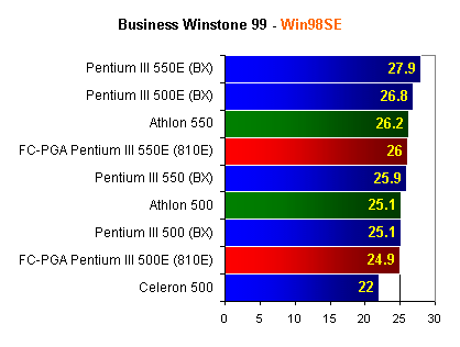
As a business performer, the FC-PGA definitely holds its own, the only reason it is any slower than the regular Pentium III E at the same clock speed is because of the i810E platform.
Business Winstone 99 |
|
Athlon 500 |
25.1 |
Athlon 550 |
26.2 |
Celeron 500 |
22 |
FC-PGA Pentium III 500E (810E) |
24.9 |
FC-PGA Pentium III 550E (810E) |
26 |
Pentium III 500 (BX) |
25.1 |
Pentium III 500E (BX) |
26.8 |
Pentium III 550 (BX) |
25.9 |
Pentium III 550E (BX) |
27.9 |
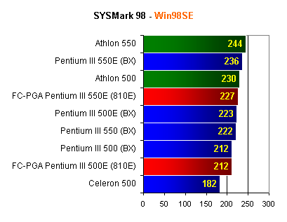
The overall performance of the FC-PGA on the i810E is still quite respectable in SYSMark 98 even though it is 4% slower than the same processor running on a BX board with the GeForce as its graphics card.
SYSMark 98 |
|
Athlon 500 |
230 |
Athlon 550 |
244 |
Celeron 500 |
182 |
FC-PGA Pentium III 500E (810E) |
212 |
FC-PGA Pentium III 550E (810E) |
227 |
Pentium III 500 (BX) |
212 |
Pentium III 500E (BX) |
223 |
Pentium III 550 (BX) |
222 |
Pentium III 550E (BX) |
236 |
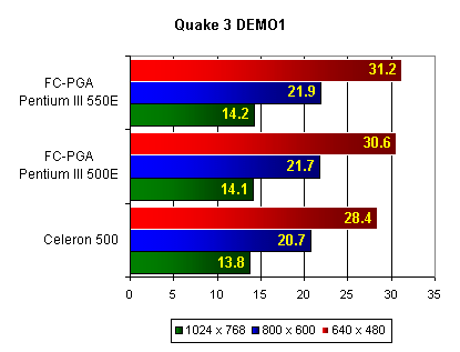
Although the image quality of the integrated i752 graphics of the 810E is excellent, the performance is definitely sub par. This is definitely not a gamer's solution.
Quake 3 DEMO1 |
640 x 480 |
800 x 600 |
1024 x 768 |
FC-PGA Pentium III 550E |
31.2 |
21.9 |
14.2 |
FC-PGA Pentium III 500E |
30.6 |
21.7 |
14.1 |
Celeron 500 |
28.4 |
20.7 |
13.8 |
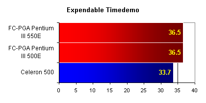
Expendable Timedemo |
640 x 480 |
FC-PGA Pentium III 550E |
36.5 |
FC-PGA Pentium III 500E |
36.5 |
Celeron 500 |
33.7 |
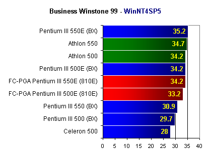
Under Windows NT the platforms with greater bandwidth do noticeably better in the benchmarks which is why the Celeron 500 is at the bottom of the list. In this case we're still dealing with business applications so even the Celeron is performing respectably.
Business Winstone 99 |
|
Athlon 500 |
34.2 |
Athlon 550 |
34.7 |
Celeron 500 |
28 |
FC-PGA Pentium III 500E (810E) |
33.2 |
FC-PGA Pentium III 550E (810E) |
34.2 |
Pentium III 500 (BX) |
29.7 |
Pentium III 500E (BX) |
34.2 |
Pentium III 550 (BX) |
30.9 |
Pentium III 550E (BX) |
35.2 |
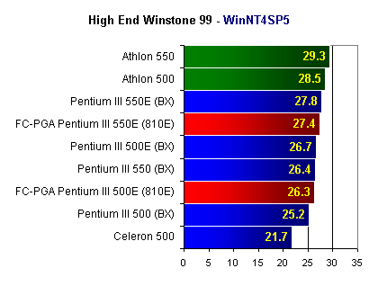
In the high-end tests where FPU power and cache speed rule, the Athlon obviously takes the top two spots, but the FC-PGA on the i810E is on the heels of the BX platform running the same CPU. For high end applications, as long as you're not doing a lot of 3D modeling, the FC-PGA may be a very affordable way to put together a low cost, high performing system under professional applications.
High End Winstone 99 |
|
Athlon 500 |
28.5 |
Athlon 550 |
29.3 |
Celeron 500 |
21.7 |
FC-PGA Pentium III 500E (810E) |
26.3 |
FC-PGA Pentium III 550E (810E) |
27.4 |
Pentium III 500 (BX) |
25.2 |
Pentium III 500E (BX) |
26.7 |
Pentium III 550 (BX) |
26.4 |
Pentium III 550E (BX) |
27.8 |
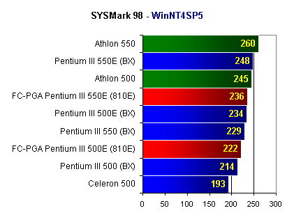
The overall performance of the i810E/FC-PGA platform under NT is also respectable with the i810E bringing the overall performance down a few percent from the same CPU running on a BX board with a GeForce (or any other current generation AGP card for that matter).
SYSMark 98 |
|
Athlon 500 |
245 |
Athlon 550 |
260 |
Celeron 500 |
193 |
FC-PGA Pentium III 500E (810E) |
222 |
FC-PGA Pentium III 550E (810E) |
236 |
Pentium III 500 (BX) |
214 |
Pentium III 500E (BX) |
234 |
Pentium III 550 (BX) |
229 |
Pentium III 550E (BX) |
248 |
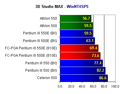
Render Times in Seconds (Lower
is Better)
The FC-PGA on the i810E manages to outpace the older Pentium III on a BX board, if the FC-PGA platform is cheaper (and it should be) then it is beginning to make sense as a low cost, high performance alternative to the Celeron and older Pentium II/IIIs.
3D Studio MAX |
|
Athlon 500 |
59.5 |
Athlon 550 |
56.7 |
Celeron 500 |
86.6 |
FC-PGA Pentium III 500E (810E) |
73.6 |
FC-PGA Pentium III 550E (810E) |
69.4 |
Pentium III 500 (BX) |
82.2 |
Pentium III 500E (BX) |
63.1 |
Pentium III 550 (BX) |
77.4 |
Pentium III 550E (BX) |
59.5 |
Conclusion
From the general trend of this review most of you would think that there is no reason to even pay any attention to the FC-PGA Pentium III E, and if you’re buying a computer today, you’d be completely right.
With the i810E as its currently only available platform, the FC-PGA would only appeal to businesses that are looking for a low cost but high performing system, thus making the FC-PGA perfect, right? Wrong.
There is a little thing called the Celeron that we’d have to ignore if the FC-PGA were to be considered a good option for businesses looking for a low cost but high performing system. The fact of the matter is that the Celeron is a fast enough solution for most applications that the FC-PGA Pentium III E really has no purpose, as long as it is coupled with the i810E platform. If Socket-370 is your only option and you’re looking for performance, the Celeron 500 is probably a better option than the FC-PGA Pentium III 500E in terms of cost. However, if you want something similarly priced to the Celeron yet faster in high end applications, the FC-PGA may interest you. For most gamers and users however, you won't be too interested by the FC-PGA on the i810E.
Then why waste time with this review? There is no difference between the FC-PGA Pentium III E and the Slot-1 Pentium III E other than the former being cheaper. So what we have here are two identical processors, one cheaper than the other, and the only thing preventing you from going out and purchasing the cheaper CPU is the fact that you’ll have to use an i810E motherboard, which is far from a high performing solution. What other options do we have?
For starters, it would take very little effort for a motherboard manufacturer to step in and update their Socket-370 designs with support for the VRM 8.4 design guidelines and offer support for the FC-PGA Pentium III E.
Here’s a question you’re probably asking: if ABIT modified the BP6 (Dual Socket-370 BX Motherboard) to support the FC-PGA Pentium III E, would it work with the FC-PGA in dual processor mode? According to Intel, no. But then again, according to Intel, the Socket-370 Celerons won’t work in dual processor mode either.
Unfortunately, we have no way of testing whether or not the FC-PGA chips are capable of running in dual processor mode. If you think about it, the FC-PGA version of the Coppermine core is no different from the SECC2 (Slot-1) version of the core and if one core is capable of working in dual processor mode, then the other one should be capable as well. At the same time, the FC-PGA has to be pin compatible with the Socket-370 Celeron so that both CPUs can be used interchangeably in a Socket-370 motherboard, so Intel could not have remapped the pins. The only possibility left is that Intel set the pin required for SMP operation to a disabled setting (SMP is enabled by default on Socket-370 Celeron CPUs but not "supported"). But with such a small population running their Celerons in dual processor mode, would Intel even spend the time to address the issue? Maybe and then again, maybe not.
The next option is the Apollo Pro 133A. We have already tested one motherboard that is based on the Apollo Pro 133A chipset; unfortunately, it did not support the VRM 8.4 specification and thus wouldn’t work with our FC-PGA CPU. The Apollo Pro 133A would be the closest match to the i820 in terms of available features. The chipset’s 133MHz FSB support could definitely come in handy if the 500Es ever made it up to 667MHz, which is entirely possible provided that the chips run cool enough. As far as the real overclocking potential of these chips is concerned, we’ll have to wait until more of them get into the hands of the users before we can make any final decisions.
As it stands right now, more platforms need to be made available before the FC-PGA Pentium III E can be recommended. Let’s just wait and see if any motherboard manufacturers step forward with the platform we’re looking for.


