Original Link: https://www.anandtech.com/show/381
Click Here to Read Even More about the i820 Chipset in our Pentium III B Review
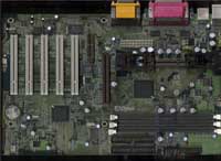
It’s the chipset we’ve all been told to wait for, and it’s finally here, the elusive "Camino" chipset has finally been released as the i820 on this day, the 27th of September in 1999.
Actually, no, it hasn’t. Due to a bug just recently discovered in the chipset, the i820 has been, as you’ve probably already heard, delayed until further notice. This is a huge hit for Intel because this is the first time they’ve truly screwed up a chipset launch. Sure, there have been delays before, but never have they come within a few days of releasing a product and had to cancel the launch due to a severe problem with stability. Could this be the market slipping through their clutches? Is it time for AMD and VIA to step in and take control of the industry?
Let’s not get too dramatic now, because, whether or not that is the case has yet to be determined and the bottom line is that Intel’s 820 has been delayed yet again. Luckily, we’ve been able to put together a comprehensive preview of the chipset to fill you all in on what you can expect from the platform when it does make its release into the market.
While we’ve all recommended waiting until the release of the i820 before pursuing a new system purchase, what you’re most likely to notice is that the "revolutionary" new chipset isn’t as groundbreaking of an introduction as we were hoping it would be.
This preview will concentrate on the i820 chipset itself and the components that go along with it and not the performance of the i820 in comparison to the BX although we will offer some comparative benchmarks between the two platforms. For a performance comparison of the new Pentium III B running on the i820 platform and the old Pentium III on the BX take a look at our Intel Pentium III 533/600B Review which covers both processors that did make it out the door today in spite of the lack of a i820 to accompany them with.
Once Again: The Accelerated Hub Architecture
The i820 chipset is the second Intel chipset to make use of their Accelerated Hub Architecture (AHA), the first being the low-cost i810. For those of you unfamiliar with the i810’s AHA, here is an excerpt from our i810 review:
The key to the success of the Accelerated Hub Architecture is the substitution of individual hub interfaces for the PCI bus in connecting the various parts of your system to your memory/CPU on the motherboard end of things. Take a look at the acronym PCI, Peripheral Component Interconnect, it doesn't really scream "all-purpose-bus" now does it? Intel took what was once a two-chip solution (North/South Bridge) and converted it into a two chip, three-hub solution, the first implementation being the i810 chipset. The three individual hubs are the Graphics and Memory Controller Hub (GMCH), the I/O Controller Hub (ICH) and the Firmware Hub (FWH). The two main hubs, the GMCH and the ICH are connected via an internal bus that offers double the bandwidth of the PCI bus, 266MB/s. This is a definite improvement over the "old" way of doing things and will shortly become the new standard as far as chipsets go, don't expect Intel to return to the classical way of doing things on the motherboard level anytime soon.
That description of the AHA is pretty much universal and applies almost in every way to the i820. The i820 differs only in its usage of the i82820 Memory Controller Hub (MCH) versus the i82810 Graphics and Memory Controller Hub (GMCH) used in the i810. The reason behind this being that the i820, unlike the 810, does not feature any integrated video, therefore removing the "Graphics" out of the Graphics and Memory Controller Hub and thus shortening it to Memory Controller Hub.
The Memory Controller Hub (MCH)
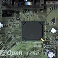 With the integrated video removed, the
i820’s MCH is a fairly simple chip that controls the system, memory and AGP buses.
The i82820 chip is the single chip that comprises the MCH and is the second desktop
chipset to be manufactured using the 0.25-micron process.
The older LX/BX chipsets were made on Intel’s 0.35-micron process and towards the end of their life cycles began requiring heatsinks on the chips. The shrink to 0.25-micron seems to have removed the requirement for a heatsink, which is why you’ll see the MCH go bare on most if not all 820 motherboards.
The MCH, unlike the previous 443BX North Bridge chipset that we’re used to, supports both the 100MHz and 133MHz FSB frequencies. This means that the whining Intel did about VIA pushing the GTL+ bus to 133MHz with their Apollo Pro 133 was meaningless because that it what Intel is doing that right now. Notice the absence of the 66MHz FSB from that listing of officially supported FSB settings.
Until we get the final word from Intel, it seems like the 66MHz FSB has finally gotten the boot, meaning that the current 66MHz FSB Celerons will not work on i820 based motherboards unless they can handle the 100MHz FSB setting. This isn’t a huge loss because in the first half of next year we will see the introduction of the first 100MHz FSB Celeron processors, the Coppermine 128.
Because of this 133MHz FSB support, the MCH now supports the ½ AGP clock divider which we were first introduced to with VIA’s Apollo Pro 133 chipset allowing for the 133MHz FSB to be used while keeping your AGP frequency at 66MHz.
Other than the 133MHz FSB support, there are two new features the MCH provides that help define the 820 chipset as a new solution. The first of those two is the AGP 4X support provided by its AGP 2.0 compliant interface.
AGP 4X Support
Looking at the AGP slot on an 820 motherboard, you’ll immediately notice the absence of the "notch" we’re used to seeing on AGP 2X cards as you can see by the picture comparison to your right. This "notch" is absent because it allows for a method of selecting the 1.5v operating voltage of an AGP 4X card instead of the 3.3v operating voltage of AGP 2X cards on which the pins, that correspond to where this notch would be located, are missing.
The 820 chipset is the first Intel chipset to boast support for the 4X transfer mode of the AGP specification which offers twice the amount of available bandwidth as the 2X transfer mode did for 1.06GB/s worth of bandwidth dedicated to your graphics adaptor alone.
Now don’t let this number fool you, because the transition from AGP 1X to AGP 2X yielded a similar theoretical performance increase and resulted in a real world performance increase that was barely noticeable. So what will the transition from AGP 2X to AGP 4X yield?
The performance numbers our benchmarks have been showing indicate a performance increase, on average, of about 0.9% in 3D games. We can easily dream up synthetic benchmarks to show off the potential of the 1.06GB/s transfer rate of AGP 4X, but until games start actually using more larger textures we won’t be seeing too much of an improvement with AGP 4X.
The one area you will probably see improvement in is where there would normally be a lot of texture thrashing to and from system memory. In this case, with an AGP 2X graphics card, you would be able to transfer textures back and forth at 528MB/s and in the case of AGP 4X that number would jump up to the 1.06GB/s we discussed earlier. As games use larger and larger textures, the performance benefits of AGP 4X will be easier to notice. But at this point in time, don’t expect to see any huge performance increase just by sticking your old TNT2 into an 820 board.
G400/TNT2 & AGP4X
Currently, the only card that we can use to test AGP 4X performance is the NVIDIA TNT2. Although the Matrox Millennium G400 and G400MAX boast AGP 4X compliance, the original G400 cards did not support the specification which was not finalized at their time of production. This unfortunately means that if you were one of the few that bought the first G400 cards, you’re stuck at a 2X transfer mode unless Matrox can come up with a workaround in the card’s firmware. Whether or not that is possible is still up to the engineers at Matrox to decide. The G400 chip itself is AGP 4X compliant.
Not even all TNT2s support 4X transfer modes. Remember all of the debate as to whether or not the TNT2 you were buying would be AGP 4X compliant from a little while back? It turns out that the same situation exists with older and newer TNT2 boards. The first sign of this was when Diamond began shipping their V770 and V770 Ultra cards with new jumpers to enable/disable AGP 4X. These cards have no problem functioning in AGP 4X mode as long as you set the jumpers properly, but the older boards without the jumpers are stuck in 2X mode unless a workaround in the firmware is developed. Whether that is possible or not still isn’t known.
The true test for AGP 4X performance will be when cards are specifically designed with the specification in mind, the first of which being NVIDIA’s GeForce 256 followed by the S3 Savage 2000 later this year. If you are interested in seeing whether or not your card will natively support the AGP 4X specification, we put a few of our TNT2s to the test to see if they passed or failed the AGP 4X test. Keep in mind that these boards are all relatively old boards and were manufactured around the release of the TNT2 chipset and the individual manufacturers may or may not have enabled AGP 4X since then on later boards.
This is by no means intended to be a comprehensive list, but it is worth looking at, especially if you were one of the first to buy any of these cards:
AGP 4X? |
|
Diamond Viper V770 (w/ AGP4X Jumpers) |
YES |
Diamond Viper V770 |
NO |
Creative Labs Graphics Blaster TNT2 Ultra |
NO |
Hercules Dynamite TNT2 Ultra |
YES |
Hercules Dynamite TNT2 |
YES |
Guillemot Maxi Gamer Xentor 32 |
YES |
Gainward CardEXPERT TNT2 |
NO |
Gainward Vanta |
NO |
Matrox G400 |
NO |
Rambus DRAM Support
The most controversial aspect of the 820 chipset is its native support for the RAMBUS DRAM or RDRAM specification. RDRAM is a new technology that Intel has been pushing in the industry for the past two years and they have just recently began talking about the standard more freely. If you look at the PC100 SDRAM that we’ve been using ever since the introduction of the i440BX chipset back in May of 1998 you can begin to realize Intel’s "need" for a higher bandwidth memory technology.
Operating at 100MHz, the PC100 SDRAM memory bus we have been used to allows for up to 800MB/s of bandwidth. While that may seem like a lot, add the fact that the AGP 4X specification is capable of transferring up to 1.06GB/s worth of data to and from the system memory over the AGP bus and you can quickly realize why a higher bandwidth memory technology is necessary.
VIA’s answer to this is the implementation of PC133 SDRAM which raises the memory bandwidth to 1.06GB/s and, in the future, their suggested PC266 DDR SDRAM should double that figure if it ever comes to market. Intel doesn’t like this option for various reasons, including the fact that they have spent quite a bit of time and money working on RDRAM and they’re not going to let that go to waste and support VIA’s standard…not yet at least.
RDRAM is a bit of a different approach to increasing available memory bandwidth. Instead of simply increasing the clock frequency by 33%, RDRAM makes use of very high speed memory, operating on a much narrower bus, resulting in a larger amount of available memory bandwidth. Let’s take a look at how we figure out the 800MB/s bandwidth provided by the memory bus at 100MHz:
(64-bit memory bus x 100MHz memory bus frequency) / 8-bits in a byte = 800MB/s
Now let’s look at what happens with RDRAM:
(16-bit RDRAM x 400MHz operating frequency x 2X data rate) / 8-bits in a byte = 1.6GB/s
Operating on a bus that’s 16-bits wide yet at a frequency of 400MHz and transferring on both the rising and falling edges of the clock (à la AGP 2X mode) and therefore doubling the effective transfer rate, RDRAM seems like the more intelligent option, right?
Not exactly. In exchange for this faster transfer rate, RDRAM sacrifices the effects of a higher latency than SDRAM, meaning that it takes longer to get the data you want from RDRAM than it does from SDRAM. At the same time, once the data is retrieved, it flows much quicker from RDRAM than it does from SDRAM courtesy of the increased transfer rates.
In some cases, RDRAM will offer a performance advantage over SDRAM, while in others it will be slower than SDRAM. In games that are doing a lot of transfers over the AGP bus (especially in 4X mode) the 1.6GB/s transfer rate of RDRAM will help get the data where it needs to go quickly. However in business applications, where there isn’t a lot of transferring of data and latency is king, then SDRAM should, in theory, reign over RDRAM.
The Different Flavors of RDRAM
RDRAM was originally only specified to operate at the 400MHz frequency while transferring on both the rising and falling edges of the clock. However, it turned out that manufacturers were having problems producing reliable RDRAM at 400MHz, so they created two lower grade versions of RDRAM, operating at 356MHz and 300MHz.
Let’s first talk about how RDRAM frequency is assigned. The speed of your RDRAM is determined by your FSB setting using a multiplier. Currently the only multipliers we’ve been able to identify are the 2.0x, 2.5x, and 3.0x RDRAM multipliers. Intel seems to indicate in their preliminary documentation that a 2.75x and 4.0x setting is present but none of the boards we’ve looked at have offered either of those two options.
If your FSB is set to 133MHz then your possible RDRAM frequencies are 266MHz (133 x 2), 333MHz (133 x 2.5), and 400MHz (133 x 3). At the same time, we don’t refer to the different RDRAM frequencies by their clock speed, rather by 2X their clock speed. So 400MHz RDRAM would be considered 800MHz RDRAM, and 333MHz RDRAM would be considered 666MHz RDRAM and so on.
When you go out to buy RDRAM, you’ll be looking for one of three types that Intel has defined:
- PC800 RDRAM – operating frequency of 400MHz
- PC700 RDRAM – operating frequency of 356MHz
- PC600 RDRAM – operating frequency of 300MHz
An interesting feature most motherboards will allow is the ability to set the frequency of your RDRAM, so if you happen to have PC600 RDRAM that can work at PC700 speeds or PC700 RDRAM that can work at PC800 speeds then setting a few jumpers should accomplish that task.
RDRAM modules, otherwise known as Rambus Inline Memory Modules (RIMMs) look very much like SDRAM modules but will not fit into the same slots for obvious reasons. They do not have to be installed in pairs, but all empty RDRAM slots must be populated by a Continuity RIMM module, or a CRIMM for short. Most motherboards will ship with at least two of these modules depending on the number of RIMM slots on-board.
Finally, due to their high operating frequency, don’t be surprised to see heatsinks on the modules themselves.
Pricing & Availability
The major downside to RDRAM (aside from the higher latency than SDRAM) is the pricing and the availability. If you thought the recent trend in SDRAM prices was insane, just wait until you begin seeing RDRAM available for sale online.
Industry analysts have been quoted as saying that the addition of an 820 based motherboard to a system (thus the addition of RDRAM) can add anywhere between $300 - $500 onto the end price of systems. While we have yet to see any 820 based systems ship yet, this initial pricing figure is quite frightening if it is any indication of the cost of implementation of RDRAM.
If RDRAM is to succeed, it has to drop in price to a reasonable level and it also must be able to be purchased by the masses. Currently, even vendors are having troubles getting RIMMs from manufacturers such as Samsung. It’ll be a while before they drop in price and increase in availability so don’t lose any sleep over waiting for that RDRAM shipment to hit anytime soon.
The I/O Controller Hub (ICH)
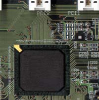 The i820 uses the same i82801AA ICH that the
i810 made use of. The 801AA provides the functions normally reserved to the South Bridge
of a chipset. Here is an excerpt from our i810 review that explains the functions of the
801AA ICH:
The ICH is the connecting force between the PCI bus, the USB ports, as well as a newcomer to the motherboard, the AMR slot. The ICH provides a direct connection to the 2 IDE channels (4 devices), the 2 USB ports, the PCI bus, and the Super I/O which drives the keyboard, mouse, FDD, serial and parallel ports.
Although there are two versions of the ICH, the ICH and the ICH0, it would be very rare that the ICH0 is used on an 820 board. The ICH, supports Ultra ATA 66/33 and supports a maximum of 6 PCI slots with an optional ISA bridge. The ICH0, supports Ultra ATA 33, and a maximum of 4 PCI slots with an optional ISA bridge. Although ISA bridges are supported by the chipset, it is highly unlikely that you'll see too many 820 boards outfitted with ISA slots.
Audio Modem Riser
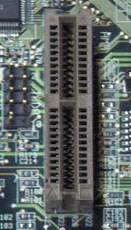 It looks like 1/3 of an AGP slot, when in
actuality it is the latest addition to the acronyms tech junkies will have to remember,
AMR, or the Audio Modem Riser slot. The AMR slot allows users to take advantage of the
chipset’s integrated Audio/Telephony codecs via a single card rather than wasting
money on a software modem (ala Winmodem).
The inclusion of the Audio/Telephony codecs allows motherboard manufacturers to produce Audio/Modem ready mainboards without having to actually test and certify the components on the Audio/Modem cards themselves. Then, after producing and releasing the board, an optional AMR card can be installed that will provide the output ports for the Audio/Telephony devices. The reason this is a more cost effective solution is because the Audio/Telephony devices are software devices that are essentially powered by your CPU. For some users, a soft modem or soft audio device makes sense, because how much of a Pentium III 600 will you be using while you're surfing the net? However, for others, it makes very little sense, such as having a soft audio/modem while playing some Quake 3 Arena on-line.
Motherboard manufacturers will be offering hardware sound/modem devices as an option as well. Chances are that hardware sound will be a preferred option by gamers since you don't usually want to waste all too many clock cycles working on producing audio when they could be boosting your frame rate.
The Firmware Hub (FWH)
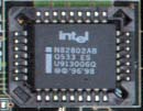 The i820 also brings over the same i82802
Firmware Hub (FWH) as used on i810 boards, and, once again, the explanation is pulled from
our original i810 review:
As you can tell by the name, the FWH is essentially the BIOS of the motherboard. The FWH is a 4Mbit EEPROM device with a bit of "intelligence" to it in that it does more than just store/retrieve predefined and modified settings, the FWH also contains Intel's own Random Number Generator (RNG). Programmers will be able to access the RNG in order to use it in developing encryption algorithms for encrypting credit card numbers for online shopping. Intel's documentation claims that the RNG is used for "greater security," go figure, regardless, the RNG is there.
There is a downside to the FWH, it happens to operate synchronously with the 33MHz PCI bus. This translates into another factor you must consider when you are overclocking the PCI bus to any degree. Although your PCI peripherals may work fine at a PCI bus frequency greater than 33%, if the FWH does not agree then you'll be in a bit of trouble. AnandTech's tests revealed that the FWH on most 820 boards is fairly reasonable when it comes to out-of-spec operation, however we issue no guarantees (it's overclocking, c'mon).
Stability Issues
The delay of the i820 chipset comes as a result of instability on motherboards with 3 RIMM slots, regardless of whether or not they are all populated. The issue does not seem to exist on boards with 2 RIMM slots, but Intel will not confirm nor deny that claim.
At this point it seems like the 820 chipset will launch with the release of Intel’s forthcoming Coppermine processor, which is how it should have been from the start. There is no point to having a 133MHz FSB Pentium III right now because the increase in performance is minimal.
The Memory Translator Hub (MTH)
We’ve mentioned before that the i820 chipset does support SDRAM but the support unfortunately does not come without its costs. In order to support SDRAM on an 820 motherboard a fourth hub must be added to the design, the Memory Translator Hub, or MTH for short.
This MTH allows for the presence of SDRAM DIMM slots on 820 boards but the performance won’t be up to par with SDRAM + BX combos, not to mention that this will obviously raise the price of a motherboard just to gain SDRAM support.
It is very clear that the i820 chipset was intended for use with RDRAM only, however, according to Intel, PC133 SDRAM support is coming in "a future chipset." Take that for what it’s worth, but it seems like Intel has something else up their sleeves.
The Test
Click
here for detailed descriptions of all of the tests run.
Click
Here for a detailed description of the four visual test modes used in the Quake 3
tests.
Windows 98 SE Test System |
|||
Hardware |
|||
CPU(s) |
Intel Pentium III 600 |
Intel Pentium III 600B Intel Pentium III 533B |
AMD Athlon 500 |
| Motherboard(s) | ABIT BX6 R2 | AOpen AX6C | FIC SD11 |
| Memory | 128MB PC133 Corsair SDRAM |
128MB PC800 RDRAM |
128MB PC133 Corsair SDRAM |
| Hard Drive | IBM Deskstar 22GXP 22GB Ultra ATA 66 HDD |
||
| CDROM | Phillips 48X |
||
| Disk Controller | Promise Ultra 66 - Ultra ATA 66 Controller |
||
| Video Card | Diamond Viper V770 Ultra clocked at 150/183MHz (core/mem) |
||
| Ethernet | Linksys LNE100TX 100Mbit PCI Ethernet Adapter |
||
Software |
|||
Operating System |
Windows 98 SE |
||
| Video Drivers | NVIDIA Reference Detonator 2.08 drivers |
||
Benchmarking Applications |
|||
Business |
Ziff Davis Winstone 99 |
||
| Gaming | idSoftware Quake 3 Test 1.08 (OpenGL) |
||
Windows NT 4 Test System |
|||
Hardware |
|||
CPU(s) |
Intel Pentium III 600 |
Intel Pentium III 600B Intel Pentium III 533B |
AMD Athlon 500 |
| Motherboard(s) | Soyo SY-D6IBA2 | AOpen AX6C | FIC SD11 |
| Memory | 128MB PC133 Corsair SDRAM |
128MB PC800 RDRAM |
128MB PC133 Corsair SDRAM |
| Hard Drive | IBM Deskstar 22GXP 22GB Ultra ATA 66 HDD |
||
| CDROM | Phillips 48X |
||
| Disk Controller | Promise Ultra 66 - Ultra ATA 66 Controller |
||
| Video Card | Diamond Viper V770 Ultra clocked at 150/183MHz (core/mem) |
||
| Ethernet | Linksys LNE100TX 100Mbit PCI Ethernet Adapter |
||
Software |
|||
Operating System |
Windows NT 4 + Service Pack 5 |
||
| Video Drivers | NVIDIA Reference Detonator 2.08 drivers |
||
Benchmarking Applications |
|||
Business |
Ziff Davis Winstone 99 |
||
Professional |
3D Studio MAX R2.5 |
||
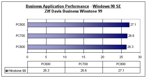
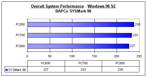
Just to point out the performance differences between the three different grades of RDRAM, we used four of our benchmarks to help illustrate.
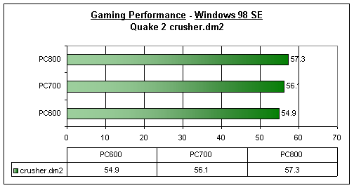
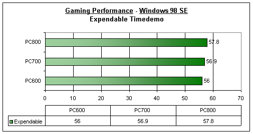
We already know that there is no visible performance increase when using AGP 4X with current game titles (sound familiar?) simply because the amount of AGP texturing is very limited to the point that we don't need 1.06GB/s worth of bandwidth. Therefore there's no point in giving you even more Quake 3 scores for AGP 4X performance.
At the same time, we have also learned that under Windows 98, the performance of the i820 chipset is either equivalent to or slower than the BX by a few percent. So where do the real performance differences emerge? In high bandwidth utilization situations, aka, under Windows NT.
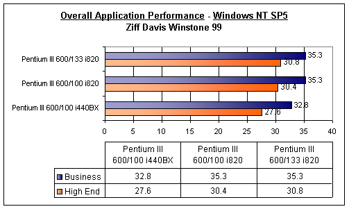
The High End Winstone 99 test proves that the PC800 RDRAM does help in the situations where a lower latency isn't going to be the deciding factor. In applications such as Photoshop and CAD Drafting applications where a lot of data needs to be moved around the RDRAM on the i820 system pulls it ahead of the BX. It is interesting to note that the use of the 133MHz FSB didn't really do all that much for the i820 test bed.
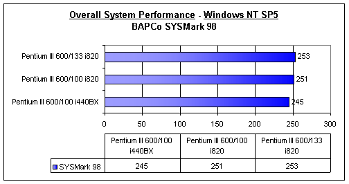
We see a similar situation here, however with the larger amount of tests run in the SYSMark 98 suite, the performance difference is more well defined.
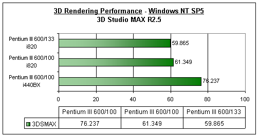
The greatest performance difference comes with the 3D Studio MAX test which is centered entirely around moving a lot of data. Once again, note the relatively tiny performance increase gained by the 133MHz FSB.
Final Words: The Future
The i820 platform has the ability to succeed, but at its current level of performance with the Pentium III B, it can’t beat AMD’s Athlon but when it pairs up with the Coppermine the competition could once again grow to be quite heated.
One thing is for sure, the i820 platform won’t be cheap and the cost is a very important factor to keep in mind. If a Coppermine + 820 platform ends up costing more than an Athlon system then Intel better hope that their Coppermine outperforms the Athlon by a good percentage. It looks like AMD may have won this battle, although a Coppermine 700 with 64KB L1 and 256KB integrated L2 cache could give the Athlon a run for its money.
So what about the weakness of the i820 chipset? RDRAM?
The theory behind RDRAM is that the only time faster memory transfer rates are necessary is when you are running an application that can’t fit entirely within a chip’s cache. In those applications, the theory holds true as we’ve proved in the benchmarks from the Photoshop and 3D Studio MAX scores in particular. When the Coppermine comes around with its 256KB of on-die L2 cache, it should be interesting to see how the matchup of the i820 and the Coppermine turns out, in terms of performance.
For overclocking, with the inclusion of the ½ AGP clock divider, a number of overclocking options once confined to our dreams have now been resurrected. Hitting the 150MHz FSB frequency shouldn’t be that big of a problem, but the main thing to remember is that the limiting factor here will again be the AGP frequency, so reaching the 160MHz FSB frequency will probably not be too successful.
What competition does the i820 have to look forward to? VIA has quietly released their AGP 4X chipset, the VT82C694X with PC133 SDRAM support instead of the RDRAM support that the i820 forces you to deal with. How will that stack up?
We’ve been playing with that chipset for a while now and you’ll be hearing more about it soon enough…
Click Here to Read Even More about the i820 Chipset in our Pentium III B Review

