Original Link: https://www.anandtech.com/show/3809/nvidias-geforce-gtx-460-the-200-king
NVIDIA’s GeForce GTX 460: The $200 King
by Ryan Smith on July 11, 2010 11:54 PM EST- Posted in
- GeForce GTX 400
- GeForce GTX 460
- GPUs
- NVIDIA
At the very end of May we saw NVIDIA’s first effort to expand Fermi beyond the $300 space with the GeForce GTX 465, a further cut-down GF100 core priced at launch at $279. Unfortunately for NVIDIA, it wasn’t even a lackluster launch – while GF100 performs quite well with most of its functional units enabled (i.e. GTX 480), disabling additional units isn’t doing the GPU any favors. Furthermore disabling those units does little to temper the chip’s high power draw – something that’s only reasonable on the higher-end cards – resulting in a card that ate a lot of power while losing to AMD’s Radeon HD 5850.
In short, the GTX 465 is a lesson of how you can only cut down GPU so far. NVIDIA went too far, and ended up with a part that had GTX 285 performance and GTX 470 power consumption.
Today NVIDIA is back in the saddle with something entirely new: GF104 and the GTX 460. The second member of the Fermi family is ready for its day in the sun, and in many ways it’s nothing like we expected. Designed from the start as a smaller chip than GF100, GF104 is the basis of the GTX 460 line of products which fix the GTX 465’s ills while delivering the GTX 465’s performance. It’s what the GTX 465 should have been, and it’s priced as low as $199. And as we’ll see, it’s the first NVIDIA card in a long time that we can give a glowing review for.
| GTX 480 | GTX 465 | GTX 460 1GB | GTX 460 768MB | GTX 285 | |
| Stream Processors | 480 | 352 | 336 | 336 | 240 |
| Texture Address / Filtering | 60/60 | 44/44 | 56/56 | 56/56 | 80 / 80 |
| ROPs | 48 | 32 | 32 | 24 | 32 |
| Core Clock | 700MHz | 607MHz | 675MHz | 675MHz | 648MHz |
| Shader Clock | 1401MHz | 1215MHz | 1350MHz | 1350MHz | 1476MHz |
| Memory Clock | 924MHz (3696MHz data rate) GDDR5 | 802MHz (3208MHz data rate) GDDR5 | 900MHz (3.6GHz data rate) GDDR5 | 900MHz (3.6GHz data rate) GDDR5 | 1242MHz (2484MHz data rate) GDDR3 |
| Memory Bus Width | 384-bit | 256-bit | 256-bit | 192-bit | 512-bit |
| Frame Buffer | 1.5GB | 1GB | 1GB | 768MB | 1GB |
| FP64 | 1/8 FP32 | 1/8 FP32 | 1/12 FP32 | 1/12 FP32 | 1/12 FP32 |
| Transistor Count | 3B | 3B | 1.95B | 1.95B | 1.4B |
| Manufacturing Process | TSMC 40nm | TSMC 40nm | TSMC 40nm | TSMC 40nm | TSMC 55nm |
| Price Point | $499 | $249 | $229 | $199 | N/A |
GF104, the heart of the GTX 460 series being launched today, is the first waterfall part of the Fermi family. As we saw with AMD’s Radeon HD 5000 series last year and NVIDIA’s GeForce 9000 series before that, NVIDIA is in the process of taking the base GF100 design and reducing it for the construction of smaller, lower performing GPUs suitable for use in video cards at lower prices for the larger markets.
The final tally for GF104 is 1.95 billion transistors, which occupies a die space slightly more than that of AMD’s Cypress in the 5800 series. To put this in comparison, this is about 200 million fewer transistors than AMD’s Cypress, or 550 million more than NVIDIA’s older GT200 GPU that powered the GeForce GTX 200 series. This makes the GF104 the biggest GPU we’ve seen for the prices NVIDIA is targeting, a sign of the increasing pricing pressure between NVIDIA and AMD.
GF104 like GF100 before it is not initially being shipped in a “full” configuration. The chip has 2 Graphics Processing Clusters (GPCs) containing 4 SMs each, for a total of 8 SMs adding up to 384 CUDA cores. The GeForce GTX 460 will be shipping with 1 of the 8 SMs disabled, leaving it with 336 enabled CUDA cores. NVIDIA tells us that the reason they’re shipping the first GF104 parts with a disabled SM is due to yields – they wouldn’t be able to meet the demand for cards if they only shipped cards with 8 functional SMs. Unlike GF100, outirght poor yields don’t appear to be a huge factor here. Our impression from discussing the issue with NVIDIA is that GF104 is yielding around where it should be for a chip of its size, with NVIDIA choosing to take a hit on selling “full” chips for a higher price in order to sell more chips overall. In any case it gives them some room for expansion in the future should they decide to release a “full” GF104 based product.
Perhaps the most surprising thing about GF104 is that it’s not a simple reduced version of GF100 like what AMD did with the Evergreen series. Instead NVIDIA made some very significant changes to the design of their SMs for GF104, resulting in a waterfall product that’s undoubtedly Fermi but also notably different from GF100. There’s a lot to discuss here, so we’ll get more in to this in a bit.
Moving on to the cards, NVIDIA is launching 2 cards today. At $229 there is the GeForce GTX 460 1GB, the closest thing we’ll see to a “full” GF104 part for the time being. The GTX 460 1GB has 7 of 8 SMs enabled along with all 32 ROPs, with a 256bit memory bus connecting the GPU to 1GB of GDDR5. The core is clocked at 675MHz core, 1350MHz shader, and 900MHz (3.6GHz effective) memory. The TDP for this part is 160W, with an unofficial idle power draw in the 20W-30W range.
The other GeForce GTX 460 being launched today is the GeForce GTX 460 768MB at $199, a slightly further cut-down card. As NVIDIA’s ROPs are closely tied to their memory controllers, the only way to reduce the amount of memory on a card is to disable memory controllers along with the ROPs. As a result the GTX 460 768MB has less memory than the GTX 460 1GB, but also only 24 ROPs connected to a 192bit memory bus. The shaders remain unchanged, giving the GTX 460 768MB the same compute/shading abilities as the GTX 460 1GB, but only 75% of the ROP capability and memory bandwidth. The clocks are unchanged from the GTX 460 1GB: 675MHz core, 1350MHz shader, and 900MHz (3.6GHz effective) memory.
Given these differences, we’re a bit dumbfounded by the naming. With the differences in memory and the differences in the ROP count, the two GTX 460 cards are distinctly different. If NVIDIA changed the clockspeeds in the slightest, we’d have the reincarnation of the GTX 275 and GTX 260. NVIDIA’s position is that the cards are close enough that they should have the same name, but this isn’t something we agree with. One of these cards should have had a different model number – probably the 768MB card with something like the GTX 455. The 1GB card does not eclipse the 768MB card, but this is going to lead to a lot of buyer confusion. The best GTX 460 is not the $199 one.
Today’s launch will be a mixed bag in terms of availability. $199 has long been known to be a critical price point with buyers, which is what makes this card so important for NVIDIA as it allows them to finally tap that market once more. However to get there they’re using their entire initial run of GF104 to build the 768MB versions of the GTX 460. There should be plenty of 768MB cards available for today’s launch, but the bulk of 1GB cards are roughly 2 weeks late (1 or 2 may show up early if the vendor does rush shipping). So what we have is a hard launch for the GTX 460 768MB, but a soft launch for the GTX 460 1GB. We’re not entirely thrilled with this – particularly as we believe the 1GB cards to be the better buy – but if nothing else it’s better than the GTX 480 launch.
Today’s launch will also be resulting in an interesting mix of price points. NVIDIA has lowered the MSRPs on the GTX 470 and GTX 465, while AMD’s prices have been slowly drifting down over the last month too. As a result we end up with roughly the following:
| July 2010 Video Card MSRPs | ||
| NVIDIA | Price | AMD |
| $700 | Radeon HD 5970 | |
| $500 | ||
|
|
$400 | Radeon HD 5870 |
| $330 | ||
|
|
$300 | Radeon HD 5850 |
| $250 | ||
| $230 | ||
| $200 | Radeon HD 5830 | |
With these prices AMD and NVIDIA both have themselves comfortably stratified until you drop below $250. AMD doesn’t have anything between the 5850 and 5830, while they have a price gap of $80-$100. Meanwhile the 5830 is priced directly against the GTX 460 768MB. NVIDIA’s pricing will be taking advantage of this gap, while giving the 5830 a run for its money at $200.
GF104: NVIDIA Goes Superscalar
When the complete GF100 GPU was presented to us back at CES 2010 in January, NVIDIA laid out a design that in turn had a very obvious roadmap to go with it. With GF100’s modular design, derivatives of the card would be as simple as fabricating GPUs with fewer GPCs and ROPs (at least until you got to the sub-$100 market). This is the route we expected NVIDIA to take with GF104, removing 1 or 2 GPCs to make a smaller chip.
What they threw us instead was a curveball we were not expecting.
Let’s start at a high level. On GF100, there were 4 GPCs each containing a Raster Engine and 4 SMs. In turn each SM contained 32 CUDA cores, 16 load/store units, 4 special function units, 4 texture units, 2 warp schedulers with 1 dispatch unit each, 1 Polymorph unit (containing NVIDIA’s tessellator) and then the L1 cache, registers, and other glue that brought an SM together.
NVIDIA GF100 - Full Implementation, No Disabled Logic
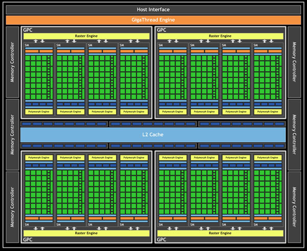
GF104 in turn contains 2 GPCs, which are effectively the same as a GF100 GPC. Each GPC contains 4 SMs and a Raster Engine. However when we get to GF104’s SMs, we find something that has all the same parts as a GF100 SM, but in much different numbers.
NVIDIA GF104 - Full Implementation, No Disabled Logic
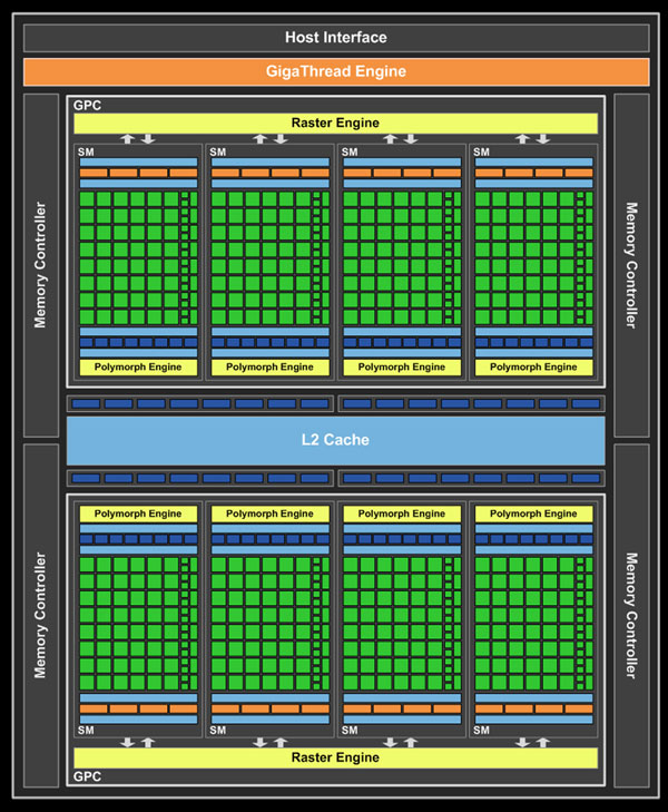
The biggest and most visible change is that NVIDIA beefed up the number of various execution units per SM. The 32 CUDA cores from GF100 are now 48 CUDA cores, while the number of SFUs went from 4 to 8 along with the texture units. As a result, per SM GF104 has more compute and more texturing power than a GF100 SM. This is how a “full” GF104 GPU has 384 CUDA cores even though it only has half the number of SMs as GF100.
One thing we haven’t discussed up until now is how an SM is internally divided up for the purposes of executing instructions. Since the introduction of G80 in 2006, the size of a warp has stayed constant at 32 threads wide. For Fermi, a warp is executed over 2 (or more) clocks of the CUDA cores – 16 threads are processed and then the other 16 threads in that warp are processed. For full SM utilization, all threads must be running the same instruction at the same time. For these reasons a SM is internally divided up in to a number of execution units that a single dispatch unit can dispatch work to:
- 16 CUDA cores (#1)
- 16 CUDA cores (#2)
- 16 Load/Store Units
- 16 Interpolation SFUs (not on NVIDIA's diagrams)
- 4 Special Function SFUs
- 4 Texture Units
With 2 warp scheduler/dispatch unit pairs in each SM, GF100 can utilize at most 2 of 6 execution units at any given time. It’s also because of the SM being divided up like this that it was possible for NVIDIA to add to it. GF104 in comparison has the following:
- 16 CUDA cores (#1)
- 16 CUDA cores (#2)
- 16 CUDA cores (#3)
- 16 Load/Store Units
- 16 Interpolation SFUs (not on NVIDIA's diagrams)
- 8 Special Function SFUs
- 8 Texture Units
This gives GF104 a total of 7 execution units, the core of which are the 3 blocks of 16 CUDA cores.
GF104 Execution Units
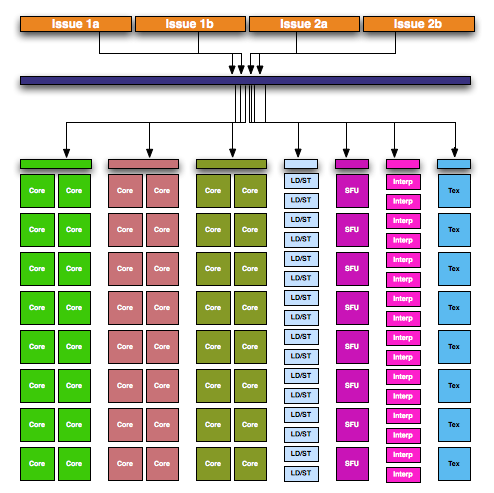
With 2 warp schedulers, GF100 could put all 32 CUDA cores to use if it had 2 warps where both required the use of CUDA cores. With GF104 this gets more complex since there are now 3 blocks of CUDA cores but still only 2 warp schedulers. So how does NVIDIA feed 3 blocks of CUDA cores with only 2 warp schedulers? They go superscalar.
In a nutshell, superscalar execution is a method of extracting Instruction Level Parallelism from a thread. If the next instruction in a thread is not dependent on the previous instruction, it can be issued to an execution unit for completion at the same time as the instruction preceding it. There are several ways to extract ILP from a workload, with superscalar operation being something that modern CPUs have used as far back as the original Pentium to improve performance. For NVIDIA however this is new – they were previously unable to use ILP and instead focused on Thread Level Parallelism (TLP) to ensure that there were enough warps to keep a GPU occupied.
NVIDIA GF100 SM
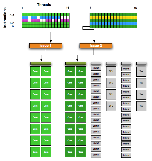
In order to facilitate superscalar operation, NVIDIA made some changes to both the warp scheduler and the dispatch unit for GF104. Each warp scheduler is now connected to 2 dispatch units, giving it the ability to dual-issue instructions. Along with its regular duties, a warp scheduler is now responsible for organizing its superscalar operation by analyzing the next instruction in its warp to determine if that instruction is ILP-safe, and whether there is an execution unit available to handle it. The result is that NVIDIA’s SMs now handle superscalar operation similar to that of a CPU, with the hardware taking the responsibility for dispatching parallel instructions. This in turn means that GF104 can execute a warp in a superscalar fashion for any code and including old CUDA code, allowing it to extract ILP out of old and new code alike. The GF104 compiler in NVIDIA’s drivers will try to organize code to better match GF104’s superscalar abilities, but it’s not critical to the ability.
NVIDIA GF104 SM - Note, more instructions in flight per SM vs. GF100
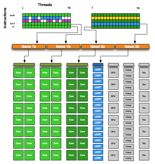
Ultimately superscalar execution serves 2 purposes on GF104: to allow it to issue instructions to the 3rd CUDA core block with only 2 warps in flight, and to improve overall efficiency. In a best-case scenario GF104 can utilize 4 of 7 execution units, while GF100 could only utilize 2 of 6 execution units.
The upside to this is that on average GF104 should be more efficient per clock than GF100, which is quite a remarkable feat. The downside to this is that now NVIDIA has a greater degree of best and worst case scenarios, as requiring superscalar execution to utilize the 3rd CUDA core block means that it’s harder to use that 3rd block than the previous 2. The ability to extract ILP from a warp will result in GF104’s compute abilities performing like a 384 CUDA core part some of the time, and like a 256 CUDA core part at other times. It will be less consistent, but on average faster than a pure 256 CUDA core part would be.
With the addition of superscalar abilities, GF104 marks the slow-but-steady merger of the CPU and the GPU. GF104 is now just a bit more CPU-like than GF100 was, a particularly interesting turn of events since we’re looking at a waterfall part and not a new architecture today.
The Rest of GF104
Besides adding superscalar dispatch abilities to GF104, NVIDIA has also made a number of other tweaks to the Fermi architecture for this GPU.
As a mid-range product, GF104 does not need to do 2 jobs at once. GF100 had to be usable as a desktop/professional graphics GPU, but also as a compute GPU for NVIDIA’s Tesla line of cards. GF104 will not be a Tesla product, so those compute abilities are not as critical. Specifically, NVIDIA has taken a chisel to Tesla’s flagship compute abilities of FP64 and ECC, which in GF100 desktop GPUs were artificially throttled and disabled respectively.
For GF104, ECC is completely gone. Barring the errant burst of solar radiation, the odds of a flipped bit or other error in the operation of a GPU is extremely slim. NVIDIA only added the feature for Tesla customers who demanded increased reliability as they could not accept a silent error in their work. For graphics however this is unnecessary, so the feature has been dropped.
Double-precision floating-point (FP64) on the other hand hasn’t been entirely dropped. Like ECC, FP64 is primarily a Tesla feature, but at the same time NVIDIA believes it to not be in their best interests to remove the feature. From NVIDIA’s perspective without FP64 on their consumer cards developers could not test and debug FP64 code on their desktops and laptops, which in turn would impede development for Tesla and hurt their efforts to expand in to the professional compute space. As a result GF104 has an interesting compromise on FP64.
For GF104, NVIDIA removed FP64 from only 2 of the 3 blocks of CUDA cores. As a result 1 block of 16 CUDA cores is FP64 capable, while the other 2 are not. This gives NVIDIA the advantage of being able to employ smaller CUDA cores for 32 of the 48 CUDA cores in each SM while not removing FP64 entirely. Because only 1 block of CUDA cores has FP64 capabilities and in turn executes FP64 instructions at 1/4 FP32 performance (handicapped from a native 1/2), GF104 will not be a FP64 monster. But the effective execution rate of 1/12th FP32 performance will be enough to effectively program in FP64 and debug as necessary.
Moving on, we have GF104’s texture units. GF100 was an interesting beast when it came to texturing, as it had texture units more efficient than GT200, but fewer of them overall. We don’t have any data that points to GF100 being absolutely deficient on texturing speeds, but at the same time it’s hard to imagine that GF100 was overbuilt to the point that losing 32 texture units wouldn’t hurt.
So for GF104, NVIDIA has doubled up on the number of texture units. A “full” GF104 has the same number of texture units at GF100 (64) in half as many SMs. NVIDIA tells us that this change is largely because texture units are small enough that they can be added without consuming too much additional die space, as opposed to requiring additional texture units such as a specific case of lacking texture performance or having too little texture performance relative to shading performance. But this isn’t something we can prove or disprove. High-detail settings optimized for high-end cards often go heavy on anti-aliasing or shading as opposed to textures, so ultimately we’re not surprised that NVIDIA kept the texture unit count constant while reducing the shader count in moving from GF100 to GF104. The shaders will be missed much less than the texture units would have been.
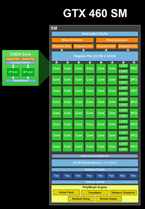
Finally, we have the ROPs. There haven’t been any significant changes here, but the ROP count does affect compute performance by impacting memory bandwidth and L2 cache. Even though NVIDIA keeps the same number of SMs on both the 1GB and 768MB of the GTX 460, the latter will have less L2 cache which may impact compute performance. Compute performance on the GTX 460 may also be impacted by pressure on the registers and L1 cache: NVIDIA increased the number of CUDA cores per SM, but not the size of the Register File or the amount of L1 cache/shared memory, so there are now additional CUDA cores fighting for the same resources. In the worst case scenarios, this can hurt the efficiency of GF104 compared to GF100.
For those of you who are curious, with all of these SM changes between GF100 and GF104 the size of a SM did increase, but by nearly as much as one would think: after adding the additional functional units, infusing the warp schedulers with superscalar dispatch capabilities, and removing unnecessary ECC and FP64 hardware, the size of an SM only increased by 25%. This is a tradeoff NVIDIA could not afford on the already massive GF100, but made sense on GF104 where the performance increase could justify the extra die space.
Meet the GTX 460
A number of differennt GTX 460 cards will be launching today. For the purpose of this article we are focusing on the reference design as it will be the most common, but there are also a number of vendor-customized designs that will be launching alongside the reference cards. For a complete writeup of the vendor cards we've received from EVGA, Asus, and Zotac, please see Part 2 of our launch day coverage.
As we discussed previously, NVIDIA will be launching 2 GTX 460 cards today: the GTX 460 1GB, and the GTX 460 768MB. The cards are virtually identical, with the latter being a GTX 460 without the 7th and 8th GDDR5 memory chips and the ROP count being adjusted accordingly. Both are otherwise built on the same PCB with the same components and same cooler.
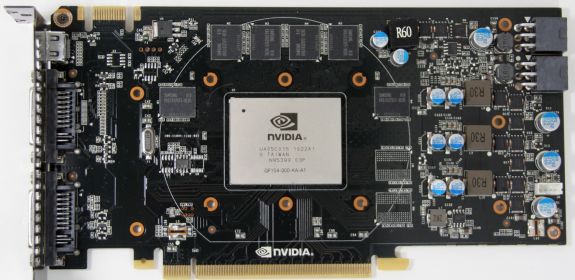
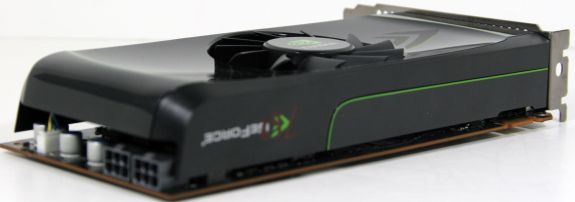
Starting with the PCB, NVIDIA has mounted a GF104 GPU on the center of an 8.25” PCB. This is a notable change from NVIDIA compared to the GTX 200 series, as the reference design for every card in that series used the same 10.5” PCB and cooling apparatus, even on the lower-end cards such as the GTX 260. On densely packed cases 10.5” could be an issue, somewhat limiting the number of cases a GTX 260 could go in to. However at only 8.25” long for the GTX 460, it’s short enough that just about any case that can accept a double-wide card can accept the GTX 460. Furthermore this makes it the shortest reference card at its price point, as the bulk of Radeon HD 5830s (which do not have a reference design) are over 8.5” long. Even the Radeon HD 5850 with its virtually identical TDP of 151W is over an inch longer.
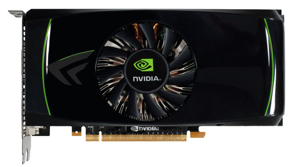
On our sample cards NVIDIA equipped the cards with 128MB 4GHz Samsung GDDR5 chips. With the cards’ memory only clocked at 3.6GHz effective this leave some room for overclocking, but as with GF100 the limit is NVIDIA’s memory controller rather than the chips. Any notable memory overclocks are just as likely to reduce performance due to error detection and retransmission as they are to improve performance.
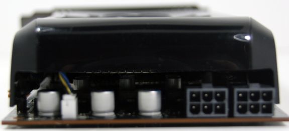
Both the 1GB and 768MB GTX 460s require 2 6pin PCIe power plugs, which are mounted facing the rear of the card. As the ATX power limit for a card with 1 plug is 150W, this makes 2 plugs required on the 160W TDP 1GB card while on the 150W TDP 768MB card it’s both a holdover from the 1GB card and an insurance bet against the card drawing more power.
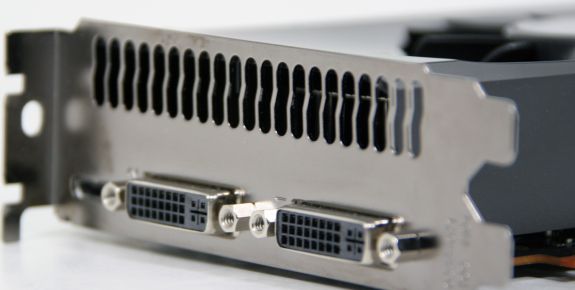
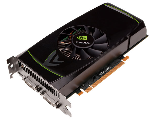
On the front of our reference cards is a port configuration identical to the reference GTX 480 and GTX 470: 2x DVI ports and a mini-HDMI port. NVIDIA went with this configuration as they believe that it’s more useful to have a mini-HDMI port than a mini-DP port due to HDMI-enabled monitors, and this hasn’t changed on the GTX 460. However like the GTX 480 and GTX 470, the GF104 GPU can only drive 2 of those 3 outputs at once.
The GTX 460 is 3DVision Surround capable just as the other GTX 400 series cards, but also like those cards this requires 2 cards in SLI to driver the requisite number of monitors. This launch effectively lowers the entry price for 3D Vision surround down from around $520 (2x GTX 465) to $400 (2x GTX 460). However we would not suggest using the feature with 768MB cards, as the extra 256MB of RAM helps a great deal at the higher resolutions created by 3DVision Surround.
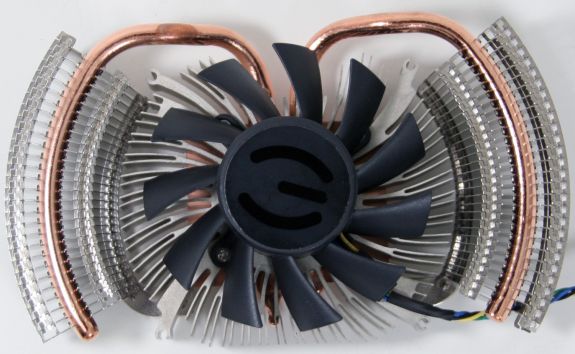
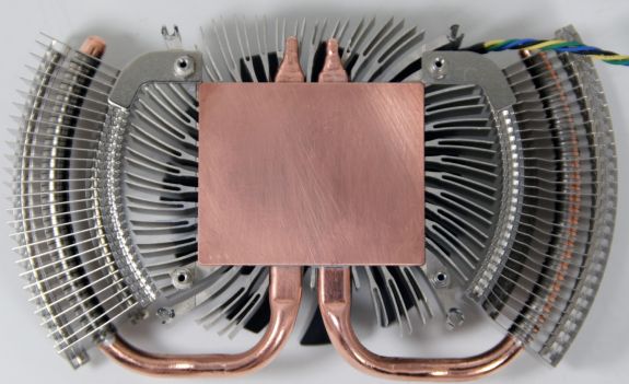
Moving beyond the PCB, we have the GTX 460’s cooler. Not unlike GF104’s revised architecture, this too caught us a bit off-guard. NVIDIA has for the longest time used a blower configuration on their mid-range and higher cards, with a rear mounted blower fully exhausting hot air outside of the case. GTX 460 deviates from this in a major way, replacing the blower with a center-mounted fan. The fan sits atop a dual-heatpipe heatsink, with the heatpipes leading to raised fins on either side of the card. In turn these heatpipes are attached to a copper base which makes contact with the heatspreader capped GPU.
As a result of this design the GTX 460 is not fully exhausting, as a center fan will push air towards both ends of the card. The rear of the card is not sealed, but the card’s cover does have a plastic lip coming down roughly as far as the fan is tall. This in turn means the blades of the fan sit at the same height as the lip, blocking direct airflow out the back. With this design the card is still exhausting at least some air out of the rear of the card, but it shouldn’t be as much as a fully-open card such as our custom Asus GTX 460. Ultimately since this isn’t a fully exhausting design, it does mean that airflow within the case is a bigger issue, but we don’t believe it’s as important as it is for fully-open cards. On the positive side, this design is well suited for use with cases that have a fan behind the card (such as on our Thermaltake Spedo), as this allows a rear fan to blow fresh air directly in to the card.
One other quirk with this design is that the plastic cover for the card is not perfectly flat, but rather it’s slightly concave. We can only surmise that this is to give the card more room to draw in air in cramped situations, although in the case of our SLI setups the covered GTX 460 still ended up running much warmer. We should also note that this only applies for cards using the reference cooler – NVIDIA isn’t requiring partners to use the reference cooler, and a number of partners will be rolling out with custom coolers.
With a $199 MSRP and 150W TDP, the 768MB GTX 460 is also the first card to be of a suitable design for HTPC use. Although we don’t expect very many GTX 460s to be used for that (rather it would be for the unannounced GF106) NVIDIA is already putting plans in to motion for HTPC cards. The GTX 460 will offer full bitstreaming audio capabilities, something the GF100 GPU powering the other GTX 400 series cards could not do. This means that the GTX 460 will be able to bitstream DTS Master Audio and Dolby TrueHD along with the 8 channel LPCM audio capabilities supported by the previous GTX 400 series cards. This brings NVIDIA up to par with AMD, who has offered bitstreaming on the entire range of Radeon HD 5000 series cards.
Much like the launch of 3D Vision Surround however, this feature is late. It is not supported in the initial shipping drivers for the GTX 460 and will be made available at a later unknown date. We’ll be sure to test it along with the rest of the GTX 460’s HTPC capabilities once it’s available.
Finally, NVIDIA has been taking an interesting marketing angle with the GTX 460. In our briefings with NVIDIA, they have been heavily promoting the overclockability of these cards, and their partners have been hard at work binning cards to take advantage of this. As a result a number of cards being launched today will have some kind of factory overclock, and there should be further headroom for end-user overclocking. NVIDIA tells us that most – but not all – cards should be good for around 800MHz core. We’ll take a look at this in-depth in our overclocking section, but of the 6 cards we have, all of them surpassed this. This won’t be like the Radeon HD 5970 where a specific overclock is practically guaranteed, but if you can put up with a bit more heat and power consumption, the odds of 800MHz or more are looking very good.
The Test
For our test we are using NVIDIA’s latest 256-series drivers, currently at version 258.80. As far as performance goes these drivers are virtually identical to earlier 256-series drivers on the GTX 400 series, so performance has not significantly changed since the launch of the drivers alongside the GTX 465. As the 256-series drivers did improve performance across a number of games for the GTX 480 and GTX 470, numbers have been updated where applicable.
As for our Radeon cards, we are continuing to use the 10.3a drivers. Radeon 5000 series performance has not changed for the games in our suite since those drivers were released.
Included in our test results are our vendor cards from Asus, Zotac, and EVGA. You can read the full review for those cards in Part 2 of our launch coverage.
For testing the GTX 460 in SLI, we used our 1GB reference card in SLI with Zotac’s 1GB card. This is suitable for performance but not for noise testing. Testing the reference 768MB GTX 460 in SLI was not possible due to the lack of a suitable matching card; however we do have the EVGA GTX 460 768MB SuperClock in SLI.
| CPU: | Intel Core i7-920 @ 3.33GHz |
| Motherboard: | Intel DX58SO (Intel X58) |
| Chipset Drivers: | Intel 9.1.1.1015 (Intel) |
| Hard Disk: | OCZ Summit (120GB) |
| Memory: | Patriot Viper DDR3-1333 3 x 2GB (7-7-7-20) |
| Video Cards: |
AMD Radeon HD 5970 AMD Radeon HD 5870 AMD Radeon HD 5850 AMD Radeon HD 5830 AMD Radeon HD 5770 AMD Radeon HD 5750 AMD Radeon HD 4890 AMD Radeon HD 4870 1GB AMD Radeon HD 4850 AMD Radeon HD 3870 NVIDIA GeForce GTX 480 NVIDIA GeForce GTX 470 NVIDIA GeForce GTX 465 NVIDIA GeForce GTX 295 NVIDIA GeForce GTX 285 NVIDIA GeForce GTX 275 NVIDIA GeForce GTX 260 Core 216 NVIDIA GeForce 8800 GT NVIDIA GeForce GTX 460 1GB NVIDIA GeForce GTX 460 768MB Zotac GeForce GTX 460 1GB Asus ENGTX460 768MB EVGA GeForce GTX 460 768MB SuperClocked |
| Video Drivers: |
NVIDIA ForceWare 197.13 NVIDIA ForceWare 257.15 Beta NVIDIA ForceWare 258.80 Beta AMD Catalyst 10.3a |
| OS: | Windows 7 Ultimate 64-bit |
Crysis: Warhead
Kicking things off as always is Crysis: Warhead, still the toughest game in our benchmark suite.Even 2 years since the release of the original Crysis, “but can it run Crysis?” is still an important question.
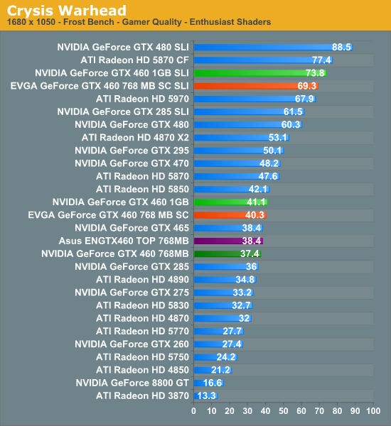
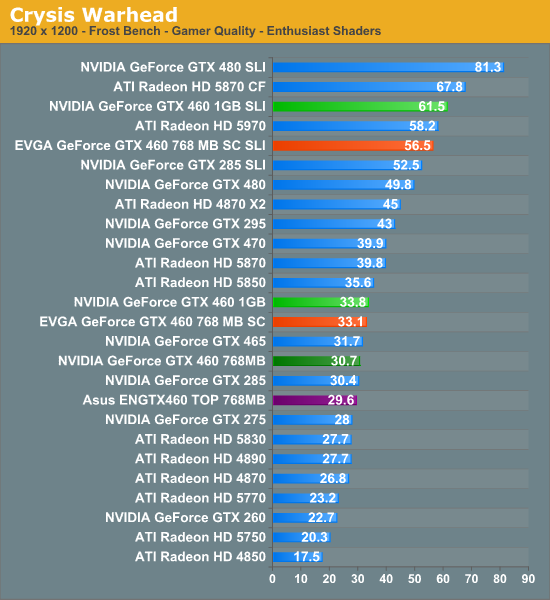
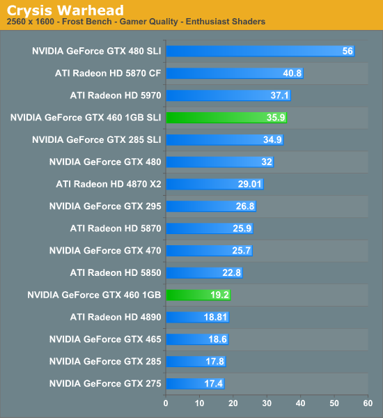
Crysis can be particularly memory-dependent, which in this case highlights the difference between the 768MB and 1GB GTX 460. 2560x1600 is not a viable option on the 768MB card here (or in most other games) due to the lack of VRAM, while at lower resolutions we can still clearly see the impact of having less RAM, less L2 cache, and less ROP power. At both 1680 and 1920, the 1GB GTX 460 is roughly 10% faster than the 768MB card. This much less than the 33% lead the 1GB GTX 460 has in terms of RAM/L2/ROP, but it’s still clear that there is a price to pay on the 768MB GTX 460.
Meanwhile the Radeon 5830 - already a hobbled card due to having half the ROPs of a full Radeon HD 5870 – takes a hard loss here. The 768MB GTX 460 comes ahead at 1920 by roughly 14% even with its RAM disadvantage. AMD definitely has their work cut out for them. As for the Radeon 5850, the 1GB GTX 460 trails right behind it until we hit 2560, where AMD’s continued advantage at high resolutions helps the card pull away some.
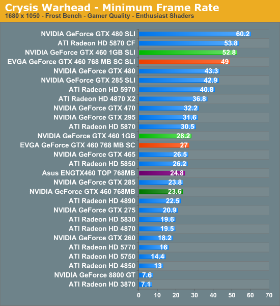
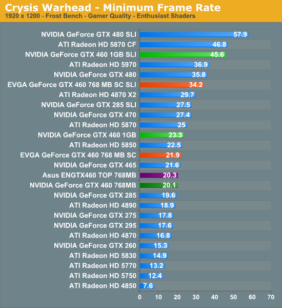
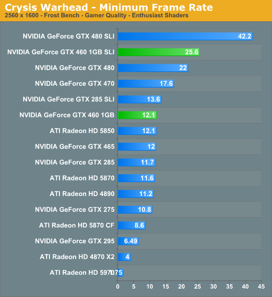
Looking at the minimum framerates, the difference in RAM/L2/ROPs becomes more pronounced. Here the 1GB GTX 460 has a 15% advantage at 1920, and strangely enough even beats a 5850 here. With the greater overhead of SLI this becomes even more of an issue, with our ragtag SLI set of 1GB GTX 460s beats our pair of factory overclocked EVGA 768MB GTX 460s by 33%. Finally the 5830 fares even worse, losing to the 768MB GTX 460 by 35%. In Crysis there is no substitute for more RAM and more ROPs.
BattleForge: DX10
Up next is BattleForge, Electronic Arts’ free to play online RTS. As far as RTSes go this game can be quite demanding, and this is just at DX10.

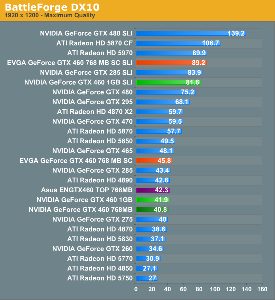
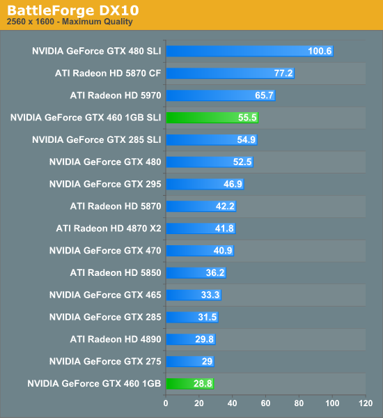
BattleForge switches things up some. No longer are we RAM/L2/ROP dependent as much as we are on raw shader power. This gives the 1GB GTX 460 only the slightest advantage over the 768MB card, while the factory overclocked cards clearly dominate here.
This also gives us a situation where we can gauge the GTX 460 and GTX 465 in a shader-bound test and see just how well the GTX 460 can do. The result in the favor of the GTX 465 by quite a bit, where it beats the 1GB GTX 460 by nearly 15%. With the need to extract ILP from the GF104 GPU to fully utilize the GPU’s CUDA cores, this looks to be approaching a worst-case scenario for the GTX 460, as it even falls behind last year’s GTX 275 and Radeon HD 4890.
As for the Radeon 5000 series, AMD’s situation improves here. The 5830 still loses, but only by 10%. Meanwhile the 5850 pulls ahead of the 1GB GTX 460 by 18%.
BattleForge: DX11
While BattleForge can be tough under DX10, under DX11 it’s even more brutal. Here we use the DX11 renderer and turn on screen space ambient occlusion (SSAO) to its highest setting, which uses a DX11 ComputeShader.
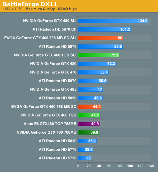
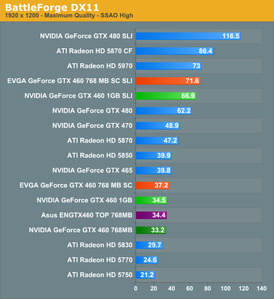
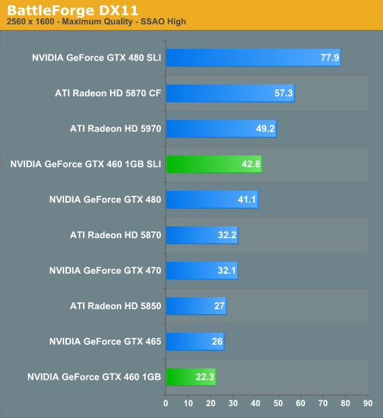
By moving to DX11 on BattleForge we can not only test a card’s shaders for graphics, but also computing through DirectCompute. The addition of a ComputeShader doesn’t seem to be benefitting anyone here, with the GTX 465 leading the GTX 460 by 15%, a tiny gap between the two GTX 460s, and finally the 5830 bringing up the rear by 11%. This will be one of the only games that favors the GTX 465 over its heir apparent.
HAWX
Ubisoft’s aerial action game is one of the less demanding games in our benchmark suite, particularly for the latest generation of cards. However it’s fairly unique in that it’s one of the few flying games of any kind that comes with a proper benchmark.
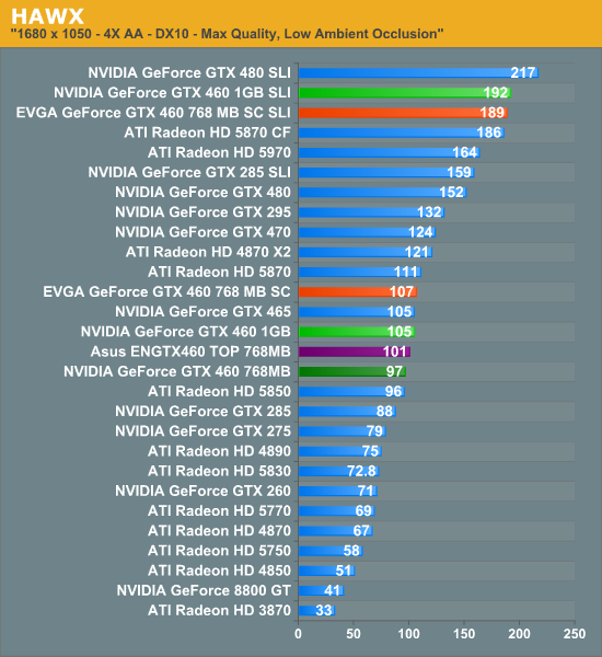
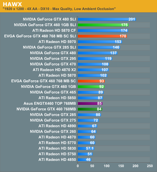
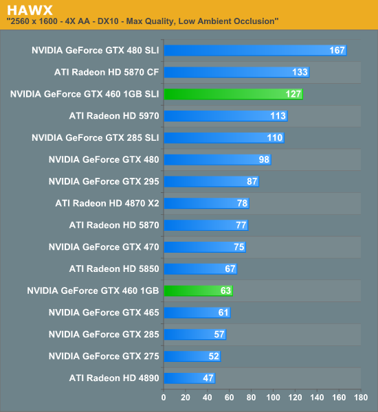
HAWX is a more balanced game and less overall demanding game, giving us yet another look at another scenario. Once more the advantages of the 1GB card shine through, while the overclocks on our other cards can close the gap. The GTX 465 once more falls to the GTX 460 1GB, and for AMD it doesn’t look good, as this is a game NVIDIA traditionally does well in. Here the 768MB GTX 460 simply crushes the 5830, and even the 5850 falls to the 1GB GTX 460.
Left 4 Dead
Introduced in 2004, Valve’s Source engine continues to live on in new Valve games. At this point even newer Source games like Left 4 Dead are rarely GPU limited to a significant degree, but we keep it on here due to the fact that we’re expecting at least one more Source game next year’s in Portal 2.
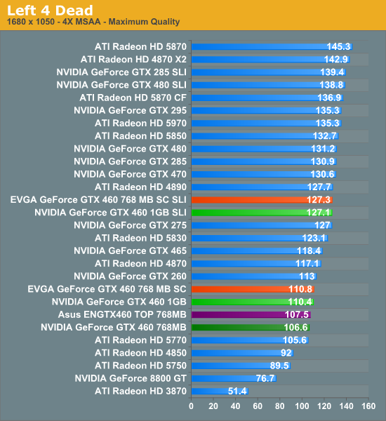
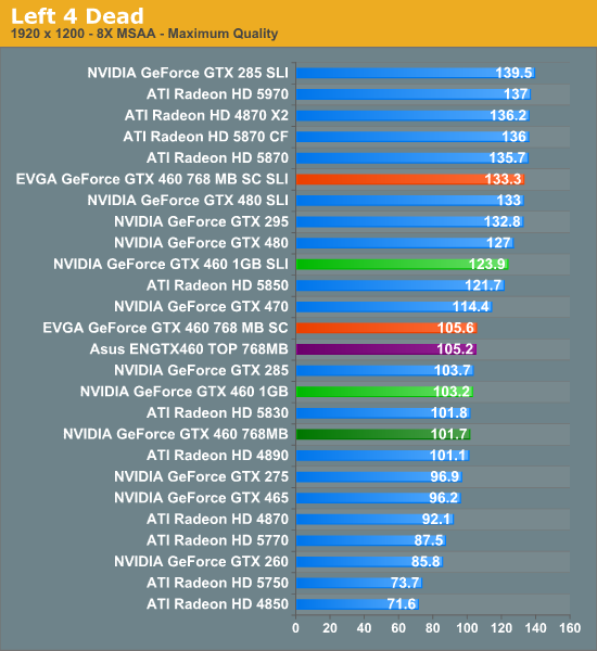
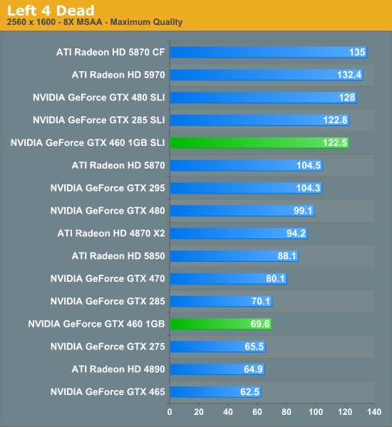
Without much of a reliance on GPUs to speak of, our cards can do little to separate themselves here. The advantages of the 1GB GTX 460 are more or less lost, and overclocking doesn’t do a great deal to separate things either. With the launch of the GTX 465 we speculated that it was held back by a lack of texturing capabilities, and these results seem to support that position, with the GTX 465 falling behind the pack by a few percent.
However this is really a game that does better under AMD’s cards. The 5830 springs to life here in a dead-heat with both GTX 460 cards, while the 5850 shoots well ahead. The GTX 460 would seem to do better on shader-heavy games than the 5830.
Battlefield: Bad Company 2
The latest game in the Battlefield series - Bad Company 2 - is another one of our new DX11 games and has been a smash hit at retail. It’s also surprisingly hard on our GPUs, enough so that we can say we found something that’s more demanding than Crysis. As BC2 doesn’t have a built-in benchmark or recording mode, here we take a FRAPS run of the jeep chase in the first act, which as an on-rails portion of the game provides very consistent results and a spectacle of explosions, trees, and more.
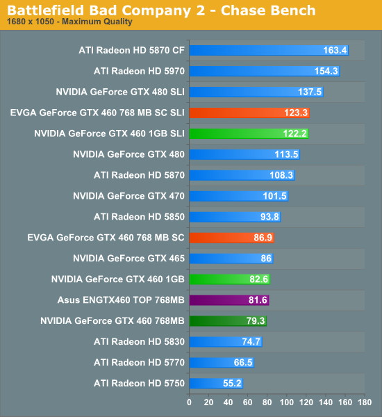
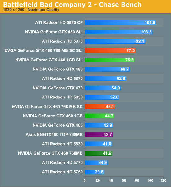
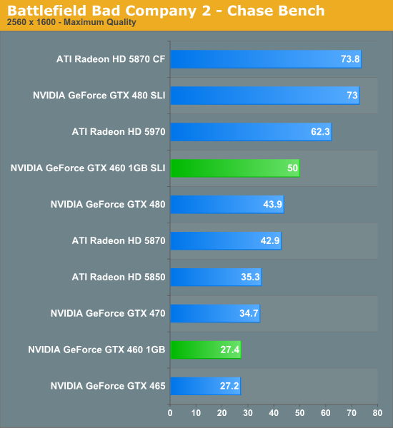
Bad Company 2 is a game where at the launch of the GTX 400 series NVIDIA started well behind before finally catching up with the 256-series driver release. It’s still not a game where they shine in, but it does at least keep them competitive. Here the Radeon 5830 basically ties the 768MB GTX 460, while the extra RAM/L2/ROP of the 1GB card gives it a 7% lead. At that delta, overclocking the GTX 460 can close the gap. Meanwhile the GTX 465 and 1GB GTX 460 return to trading blows, with the GTX 460 edging out the GTX 465.
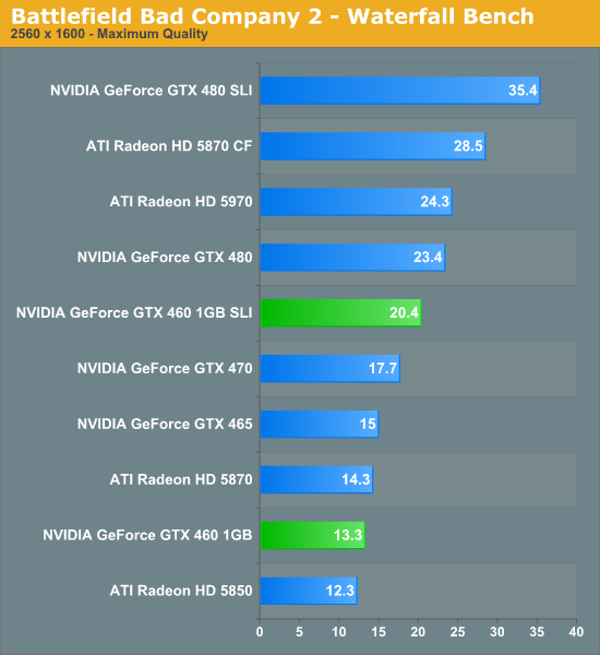
As for our worst case scenario Bad Company 2 waterfall benchmark, we get an interesting shakeup. As has been the case with the other GTX 400 series cards, the 1GB GTX 460 does better here than it does on the Chase benchmark, putting it between the Radeon 5850 and 5870. However in turn the GTX 465 edges the GTX 460 out for a slight lead, in which case we’re probably shader bound.
STALKER: Call of Pripyat
The 3rd game in the STALKER series continues to build on GSC Game World’s X-Ray Engine by adding DX11 support, tessellation, and more. This also makes it another one of the highly demanding games in our benchmark suite.
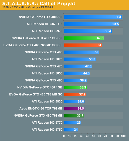
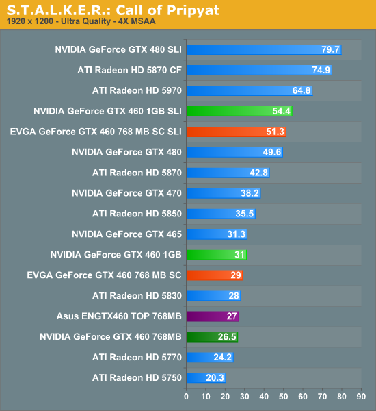
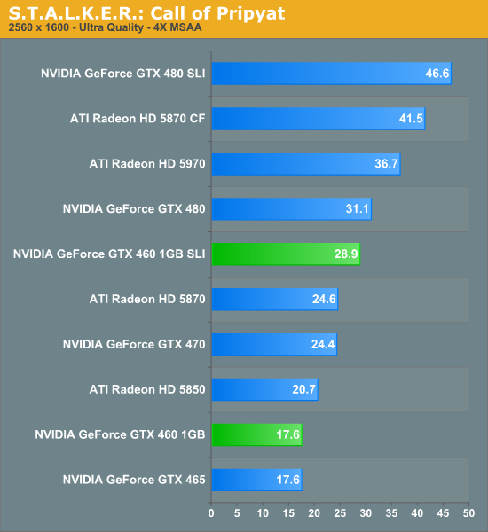
With the launch drivers for the GTX 465 it ended up taking a nosedive in this game. That has since been resolved, giving us another close competition between the GTX 465 and GTX 460. Here the 1GB GTX 460 is neck-and-neck with the GTX 465, while the 768MB GTX 460 suffers for its lack of RAM/L2/ROP, letting the 1GB card pull ahead by 17%. This also results in the GTX 465 falling to the Radeon 5830 by around 5%.
DIRT 2
Codemasters latest racing game marks the return of a racer to our benchmark suite. As the first DX11 racer, DIRT 2 makes pretty through use of the DX11’s tessellation abilities, not to mention being the best looking racer we have ever seen.
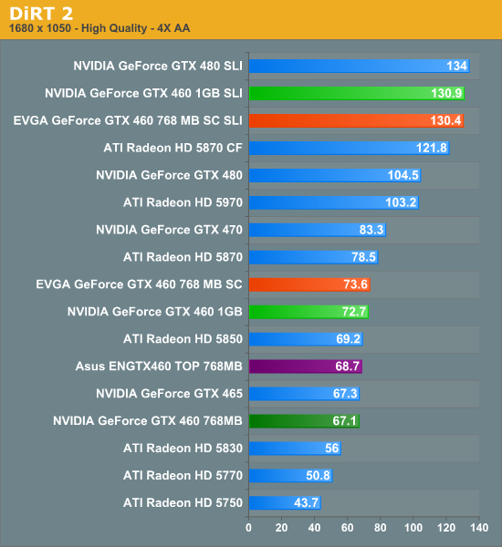
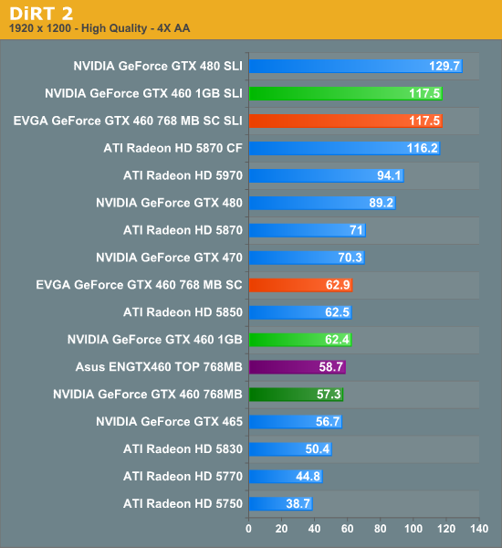
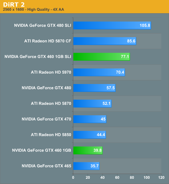
DIRT 2 is a game that NVIDIA’s cards do well at, so long as they’re not overly crippled like the GTX 465. Here the 1GB GTX 460 is effectively tied with the Radeon 5850, while the 768MB GTX 460 trampled the 5830 by 14%. Among NVIDA’s cards the 1GB GTX 460 pulls off a 9% advantage over its cheaper sibling, and the GTX 465 falls to even the 768MB GTX 460 here by a frame.
We’re also seeing the first signs of being CPU limited, with a pair of GTX 460s coming to within 10% of a pair of GTX 480s.
Mass Effect 2
Electronic Arts’ space-faring RPG is our Unreal Engine 3 game. While it doesn’t have a built in benchmark, it does let us force anti-aliasing through driver control panels, giving us a better idea of UE3’s performance at higher quality settings. Since we can’t use a recording/benchmark in ME2, we use FRAPS to record a short run.
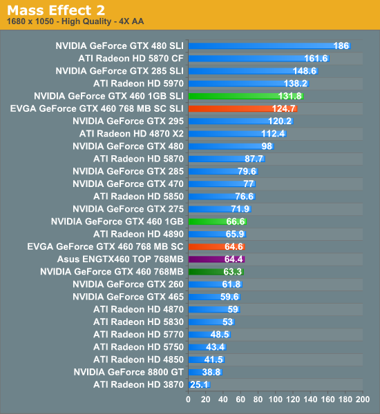
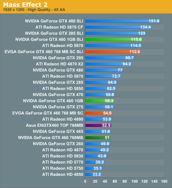
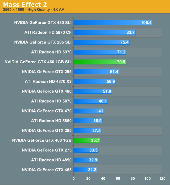
Mass Effect 2 ends up being another game with a lot of stratification. Working our way from the top the 1GB GTX 460 has a clear advantage over the 768MB GTX 460 even with an overclock, giving it a 15% lead at stock clock speeds. Meanwhile the 768MB GTX 460 has a 16% lead over its equally priced competitor, the 5830. In spite of the 5830 taking a sizable loss here though, the 5850 keeps a 7% lead over the closest GTX 460, while the GTX 465 is at parity with the 768MB GTX 460.
Curiously, we’re still seeing something we saw with the GTX 465 at its launch: the stellar performance of the GTX 285. Even with the 1GB GTX 460’s better performance over the GTX 465, it still loses to the GTX 285.
Wolfenstein
Finally among our revised benchmark suite we have Wolfenstein, the most recent game to be released using the id Software Tech 4 engine. All things considered it’s not a very graphically intensive game, but at this point it’s the most recent OpenGL title available. It’s more than likely the entire OpenGL landscape will be thrown upside-down once id releases Rage next year.
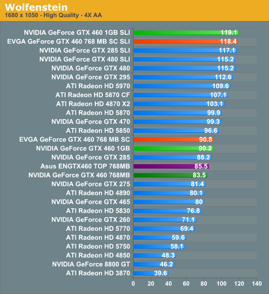
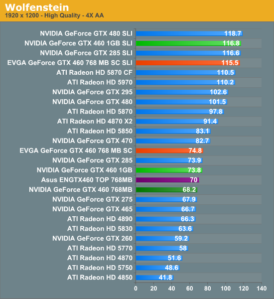
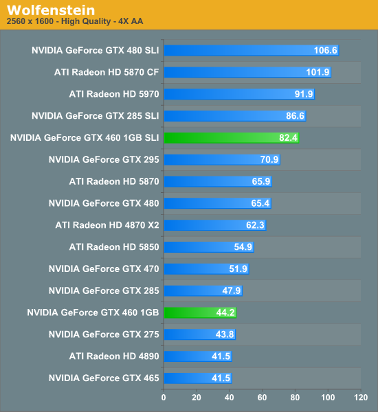
Light on the shader use, this game is more about the ROPs, which returns unsurprising results. The 1GB GTX 460 enjoys an 8% lead over the 768MB version, while the 768MB version enjoys a 7% lead over the 5830. Overclocking is fairly effective here, with the factory overclocked EVGA GTX 460 pulling ahead of the 1GB reference GTX 460.
Compute & Tessellation Performance
With our earlier discussion on the GF104’s revised architecture in mind, along with our gaming benchmarks we have also run a selection of compute and tessellation benchmarks specifically to look at the architecture. Due to the fact that NVIDIA added an additional block of CUDA cores to an SM without adding another warp scheduler, the resulting superscalar design requires that the card extract ILP from the warps in order to simultaneously utilize all 3 blocks of CUDA cores.
As a result the range of best case to worst case scenarios is wider on GF104 than it is GF100: while GF100 could virtually always keep 2 warps going and reach peak utilization, GF104 can only reach peak utilization when at least 1 of the warps has an ILP-safe instruction waiting to go, otherwise the 3rd block of CUDA cores is effectively stalled and a GTX 460 performs more like a 224 CUDA core part. Conversely with a total of 4 dispatch units GF104 is capable of exceeding GF100’s efficiency by utilizing 4 of 7 execution blocks in an SM instead of 2 of 6.
Or in other words, GF104 has the possibility of being more or less efficient than GF100.
For our testing we’re utilizing a GTX 480, a GTX 465, and both versions of the GTX 460, the latter in particular to see if the lack of L2 cache or memory bandwidth will have a significant impact on compute performance. Something to keep in mind is that with its higher clockspeed, the GTX 460 has more compute performance on paper than the GTX 465 – 907GFLOPs for the GTX 460, versus 855GFLOPs for the GTX 465. As such the GTX 460 has the potential to win, but only when it can extract enough ILP to keep the 3rd block of CUDA cores working. Otherwise the worst case scenario – every math instruction is dependent – is 605GFLOPs for the GTX 460. Meanwhile the GTX 480 is capable of 1344GFLOPs, which means the GTX 465 and GTX 460 are 63% and 45%-67% as fast as it on paper respectively.
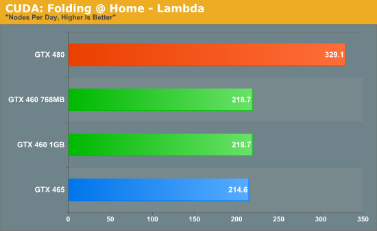
We’ll start with Stanford’s Folding@Home client. Here we’re using the same benchmark version of the client as from our GTX 480 article, running the Lambda work-unit. In this case we almost have a tie between the GTX 460 and the GTX 465, with the two differing by only a few nodes per day. The GTX 465 reaches 65% of the performance of the GTX 480 here, which is actually beyond the theoretical performance difference. In this case it’s likely that the GTX 480 may be held back elsewhere, allowing slower cards to shorten the gap by some degree.
With that in mind the GTX 460 cards achieve 66% of the performance of the GTX 480 here, giving them a slight edge over the GTX 465. Because we’ve seen the GTX 465 pull off better than perfect scaling here it’s very unlikely that the GTX 460 is actually achieving a perfect ILP scenario here, but clearly it must be close. Folding@Home is clearly not L2 cache or memory bandwidth dependent either, as the 768MB version of the GTX 460 does no worse than its 1GB counterpart.
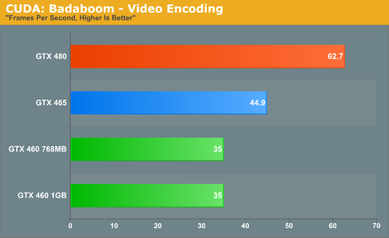
Next up on our list of compute benchmarks is Badaboom, the CUDA-based video encoder. Here we’re measuring the average framerate for the encode of a 2 minute 1080i video cap. Right off the bat we’re seeing dramatically different results than we saw with Folding@Home, with the GTX 460 cards falling well behind the GTX 465. It’s immediately clear here that Badaboom is presenting a sub-optimal scenario for the GTX 460 where the GPU cannot effectively extract much ILP from the program’s warps. At 56% the speed of a GTX 480, this is worse off than what we saw with Folding@Home but is also right in the middle of our best/worst case scenarios – if anything Badaboom is probably very close to average.
Meanwhile this is another program with the lack of memory bandwidth and L2 cache is not affecting the 768MB card in the slightest, as it returns the same 35fps rate as the 1GB card.
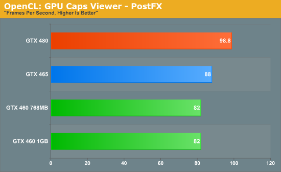
Our third and final compute benchmark is the PostFX OpenCL benchmark from GPU Caps Viewer. The PostFX benchmark clearly isn’t solely compute limited on the GTX 400 series, giving us a fairly narrow range of results that are otherwise consistent with the Badaboom. At 82fps, this puts the GTX 460 below the GTX 465 by around 7%, once again showcasing that the superscalar GTX 460 has more trouble achieving its peak efficiency than the more straightforward GTX 465.
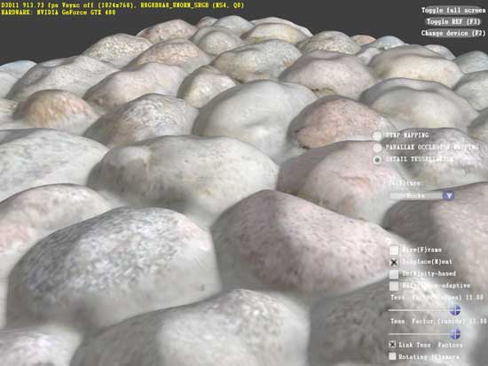
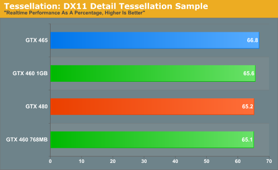
Our final benchmark is a quick look at tessellation. As GF104 packed more CUDA cores in to a SM, the GPU has more than half the compute capabilities of GF100 but only a straight 50% the geometry capabilities. Specifically, the GTX 460 has 45% of the geometry capabilities of the GTX 480 after taking in to account the number of active SMs and the clockspeed difference.
With the DirectX 11 Detail Tessellation sample program, we’re primarily looking at whether we can throw a high enough tessellation load at the GPU to overwhelm its tessellation abilities and bring it to its knees. In this case we cannot, as the GTX 460 scales from tessellation factor 7 to tessellation factor 11 by basically the same rate as the GTX 480 and GTX 465. This means that the GTX 460 still has plenty of tessellation power for even this demanding sample, but by the same measure it showcases than the GTX 480 is overbuilt if future games target GTX 460 for tessellation.
All things considered our compute and tessellation results are where we expected them to be. That is to say that the GTX 460’s wider range of best and worst case scenarios will show up in real-world programs, making its performance relative to a GTX 465 strongly application dependent. While the GF104 GPU’s architectural changes seem to be well tuned for gaming needs and leading to the GTX 460 meeting or beating the GTX 465, the same can’t be said for compute. At this point it would be a reasonable assumption that the GTX 465 is going to outperform the GTX 460 in most compute workloads, so the relevance of this for buyers is going to be how often they’re doing compute workloads and whether they can deal with the GTX 465’s lower power efficiency.
Power, Temperature, & Noise
As we’ve discussed in previous articles, with the Fermi family GPUs no longer are binned for operation at a single voltage, rather they’re assigned whatever level of voltage is required for them to operate at the desired clockspeeds. As a result any two otherwise identical cards can have a different core voltage, which muddies the situation some. All of our GTX 460 cards have an idle voltage of 0.875v, while their load voltage is listed below.
| GeForce GTX 460 Load Voltage | |||||
| Ref 768MB | Ref 1GB | EVGA 768MB #1 | EVGA 768MB #2 | Asus 768MB | Zotac 1GB |
|
0.987v
|
1.025v
|
0.987v
|
1.000v
|
0.987v
|
1.000v
|
Our cards end up ranging from 0.975v to 1.025v, a variance of 0.05v. The 1GB cards with additional functional units on average require more voltage to operate, with the lowest of our samples requiring 1.0v. Otherwise 3 of our 4 768MB cards require 0.975v.
On a side note, since we’re using non-matching 1GB GTX 460s here for SLI testing, we’ve added an asterisk for all the power & temperature results. Our results should be very close to what a proper set of matching reference cards would get, but we can’t guarantee that.
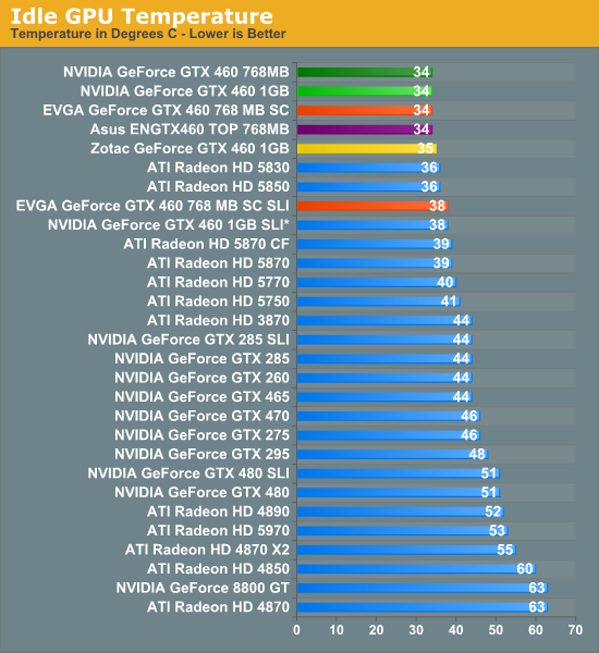
We’ll start with idle temperatures. With an unofficial idle TDP in the 20W range, the GTX 460 series is fairly comparable to the Radeon 5850, but with a more breezy cooler. As a consequence we can see it edge out the rest of our cards here, with all of the open GTX 460s coming in at 34C for idle. Meanwhile the blower-based Zotac card comes in a hair warmer at 35C. Even with a blower, these end up being the coolest mid-range or better cards we have ever tested, besting even the Radeon 5850.
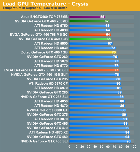
Meanwhile at load the good news continues for the GTX 460 series. The GTX 480 may have been a toasty GPU, but that’s not the case for the GF104 GPU at the heart of the GTX 460 series. Our reference cards do only slightly worse than 60C in Crysis, while Asus’s non-reference card gets that even lower thanks to a more proactive fan. Zotac’s blower doesn’t fare so well here though, coming in at a still respectable but nevertheless higher 73C.
Compared to AMD’s cards the GTX 460 does very well here. The Radeon 5850 is still the sweet spot for a balance of performance and heat, but the GTX 460 manages to do better in terms of heat at a price of lower gaming performance. Meanwhile our Radeon 5830 isn’t even a contender here; as a salvaged Cypress part, it just can’t compete with a part designed for cooler performance from the start. Among all the cards we’ve tested equal to or faster than the 8800GT however, the GTX 460 sets the new bar for how cool a high performance card can operate.
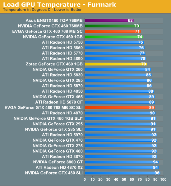
The results with Furmark match those of Crysis, it’s just a bit hotter. The interesting story here is going to be SLI temperatures: our 768MB and 1GB SLI cards hit 89C and 91C respectively. This isn’t a problem for NVIDIA’s GPUs (we see single GTX 480 cards do worse) but it’s a massive jump from a single card. For these reasons we would strongly suggest keeping these cards further spaced apart if you have a motherboard that supports it. The GTX 460 reference cooler just isn’t up to the task of pulling in fresh air if it’s next to another card.
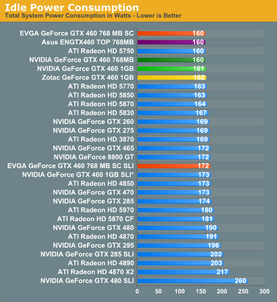
Our idle power numbers continue to lower the bar for GPUs of this performance class, although at this point we’re hitting the efficiency limits of our PSU at low wattages. Our 768MB GTX 460s end up sharing the 160W mark with the Radeon HD 5750, while for 1W more you have the 1GB cards.
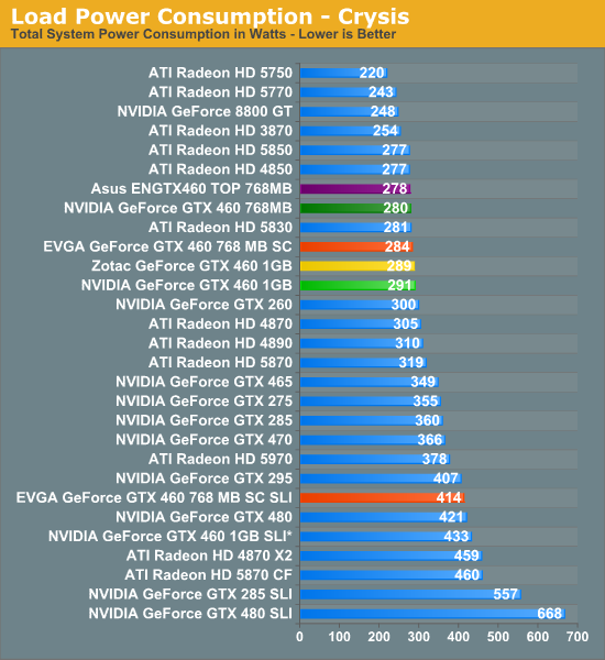
When looking at load power consumption, it’s always interesting to compare the power drawn with the temperatures. While the GTX 460 did very well here with regard to temperature, its power consumption reflects the fact that its GPU is still Cypress-sized. Under Crysis at a 280W load the 768MB part is comparable to the Radeon 5830 and the 1GB part adds around 10W to that. Meanwhile the Radeon 5850 manages to pull just a bit less power here, while the GTX 465 draws some 60W-70W more than the GTX 460. Gmae performance with those two cards may be close – power consumption is not.
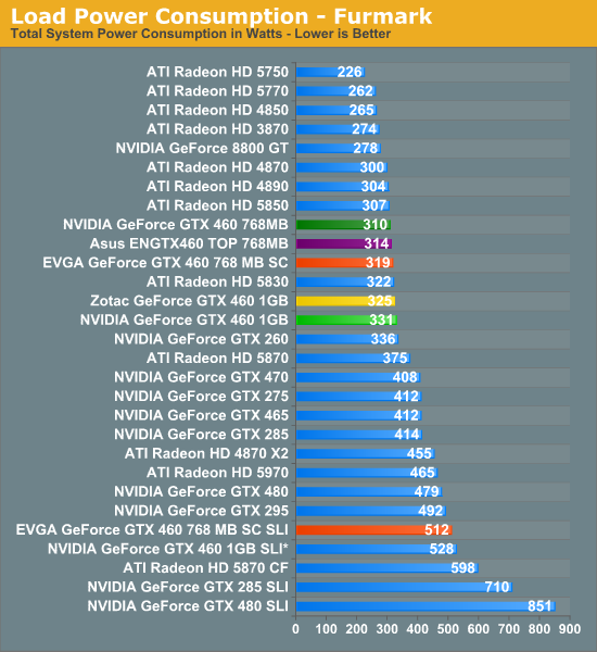
As for Furmark the power consumption goes up but the ordering does not. Our 1GB cards now draw 20W more than 768MB cards, but the Radeon 5830 is still in the middle of the pack while the Radeon 5850 comes out ahead. The GTX 465 is now 80W-100W hotter than the GTX 460. Overall with a “proper” Radeon 5000 series card NVIDIA still can’t match AMD on a performance per watt basis, but they can come very close.
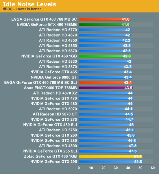
Finally we have our look at noise. With cool running cards we often have to look at fan noise to ensure that they aren’t accomplishing that trick by sounding like a jet engine, and in the case of the GTX 460 that’s clearly not the case. Besides being some of the coolest cards we’ve tested at this performance level the GTX 460 cards are also just as quiet as the rest of the best of the cards we’ve tested, hugging the 42dB sound floor in our testing environment. The 1GB reference card is marginally louder, while the partner customized cards are only slightly louder yet. The only card to really flop here is the Zotac GTX 460, which is at entirely the wrong end of our charts. Blowers can be quiet, but the Zotac’s is not – it’s simply a loud card. Unfortunately this kind of an idle noise level is going to put the card out of the running for a lot of buyers.
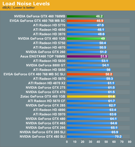
Load noise is more or less like our idle noise results. The 768MB GTX 460 registers the lowest result we’ve ever seen for a card of this performance level, coming in at 46.2dB and the EVGA card right behind it. The 1GB card does end up being louder (likely to compensate for cooling 2 more GDDR5 chips) but it’s still in good company. Asus’s card cracks 50dB, as it’s tuned for cooling over noise, explaining our earlier temperature results. Unfortunately the Zotac card is once again the odd man out at 61dB, roughly as loud as our GTX 470 is. It’s neither cooler than our reference cards nor quieter, which doesn’t bode well for this stock-clocked card.
Overclocking
Last but not least on our tour of the GeForce GTX 460 is a look at the overclocking abilities of the card. As we discussed earlier, NVIDIA is heavily promoting the overclockability of the card to the press, proclaiming that they are regularly able to get most cards up to 800MHz. We’re in a unique situation today to put that to the test, as along with our 2 reference cards, we have an additional 4 vendor cards from our GTX 460 roundup to tinker with. With 6 cards on hand we have a non-definitive but still very useful sample set to work with to verify just how overclockable these cards are, and what kind of a power penalty this entails.
For the purposes of this section we are focusing on the overclockability of the core, but not the memory. NVIDIA’s weaker GDDR5 memory controller coupled with the tendency for memory overclocking to reduce performance through the need to use error detection and retransmission makes memory overclocking much more difficult and often a bust entirely.
As not all of our cards are exactly alike, we’ll quickly run down the differences between the various cards
- 1x NVIDIA GTX 460 768MB Reference
- 1x NVIDIA GTX 460 1GB Reference
- 2x EVGA GTX 460 768MB SuperClocked: Reference PCB and cooler, factory overclocked
- 1x Zotac GTX 460 1GB: Reference-derived PCB, custom blower-style cooler
-
1x Asus ENGTX460 768MB TOP: Custom PCB, custom cooler, factory overclocked, voltage tweak
| Stock Clock | Max Overclock | Stock Voltage | Overclocked Voltage | |
| GTX 460 768MB Reference | 675MHz | 840MHz | 0.987v | N/A |
| GTX 460 1GB Reference | 675MHz | 825MHz | 1.025v | N/A |
| EVGA GTX 460 768MB SuperClocked #1 | 763MHz | 850MHz | 1.000v | N/A |
| EVGA GTX 460 768MB SuperClocked #2 | 763MHz | 840MHz | 0.975v | N/A |
| Zotac GTX 460 1GB | 675MHz | 835MHz | 1.000v | N/A |
| Asus ENGTX460 768MB TOP | 700MHz | 930MHz | 0.975v | 1.062v |
| GTX 460 1GB SLI | 675MHz | 800MHz | N/A | N/A |
| EVGA GTX 460 768MB SuperClocked SLI | 763MHz | 840MHz | N/A | N/A |
Among our 5 cards without voltage tweaking capabilities, all of the cards are closely clustered together in terms of the final stable overclock, with only a 25MHz difference between the top and bottom cards. The 1GB cards ended up with slightly lower overclocks than the 768MB cards, which is likely a product of the 1GB cards containing further enable ROPs and L2 cache than the 768MB cards. Meanwhile the best overclock on a card we got without a voltage tweak was one of our EVGA cards, which was able to go to 850MHz. On average we were able to attain a 24% overclock over the GTX 460 reference clock of 675MHz, and in the case of the EVGA cards a 10% overclock over their factory speed of 763MHz.
The lone standout in the group is the Asus card, which has voltage tweaking capabilities that allow us to increase the core voltage beyond the GPU’s VID. Asus’s SmartDoctor software allows for the card to be overvolted to 1.087v in 0.0125v increments, however in testing we found that anything over 1.062v would ultimately cause the card to fall back to 405MHz, which we believe to be the card’s VRM protection kicking in after the VRMs overheated. At 1.062v we were able to get the card to up 930MHz, a 33% overclock from the factory overclocked speed of 700MHz, and 38% faster than the GTX 460 reference clock of 675MHz.
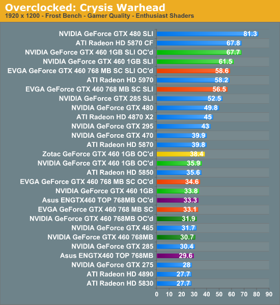
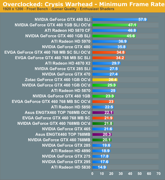
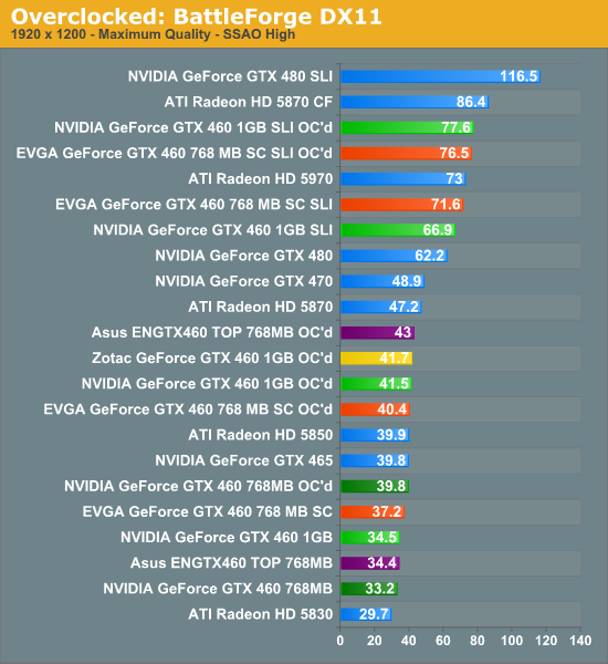
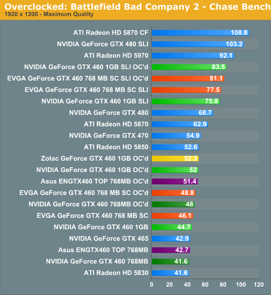
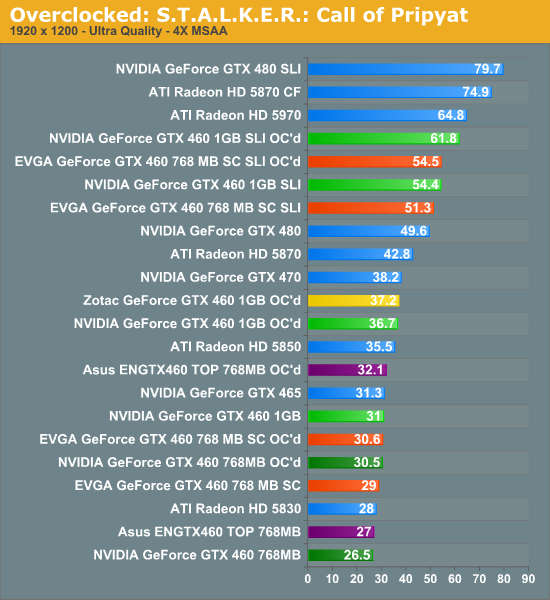
Overall the impact of overclocking is heavily game dependent. Core overclocking favors games that are ROP/shader limited and has little effectiveness on games that are limited by the total available RAM or by memory bandwidth. For this reason out of our subset of games core overclocking was most effective on Battleforge and Bad Company 2, while only moderately effective on Crysis and STALKER. On Crysis and STALKER overclocking was at best only marginally more useful than having a 1GB card. And even with its greater core overclock, the Asus ENGTX260 is not immune to this effect once the 1GB cards are overclocked – it still falls behind an overclocked 1GB card ¾ of the time.
Currently the sweet spot would look to be a 1GB card with a lesser overclock. The additional RAM/L2/ROPs more than makes up for the higher overclocks the 768MB cards can attain in most situations.
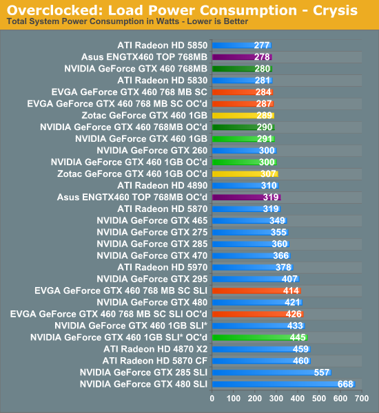
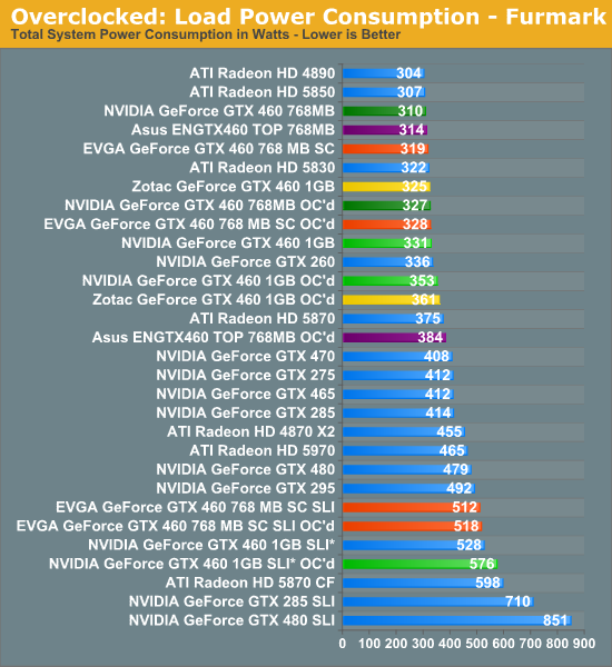
For the cards without voltage tweaking capabilities, the power consumption penalty for overclocking is very minor due to the fact that power consumption increases with voltage much faster than it does with frequency. For the stock-clocked cards this is a 15W-25W penalty, while the factory overclocked cards are even lower (thanks to binning) at just 9W. Meanwhile as expected the Asus card with its voltage tweaking capabilities ends up witnessing a larger jump in power consumption in return for its greater overclock capabilities: 70W.
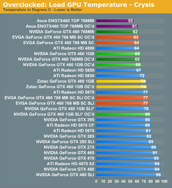
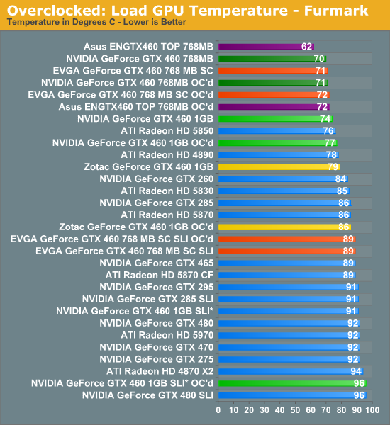
With only a minor increase in power consumption and the use of very efficient coolers, the GTX 460 only experiences a minor rise in temperature when overclocking without voltage modification. All of our cards with the exception of the Zotac under Furmark only rise in temperature by a few degrees, leaving temperatures well in the safe range for these cards. Even the Asus card with voltage modification stays fairly cool thanks to its more aggressive fan, rising by up to 10C under Furmark but still only becoming as warm as our stock-cooled cards in the first place.
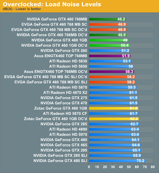
Last but not least we have the noise factor. Thanks to the very low increase in power consumption these cards experience when overclocking, the coolers on these cards have to do very little to handle the extra heat. For the cards without voltage modding, the amount of noise generated increased by less than 1.5dB, and in the case of our EVGA cards didn’t increase at all. This results in our GTX 460 cards remaining as some of the quietest mid and high-end cards we’ve ever benchmarked, even with a 24% overclock.
The Asus card is of course the exception to the rule here, once again due to a combination of the more aggressive cooler and voltage modification. Here the amount of noise generated shoots up by 4.4dB when overclocked, which is a fair trade for the overclock but is definitely going to be more noticeable than the rest of the cards in our collection.
With all of this taken in to consideration, there’s little we can do to argue with NVIDIA’s claims about the GTX 460’s overclocking capabilities. One thing we need to make clear before going any further though is this: overclocking is not guaranteed. In our briefings with NVIDIA, they have told us that they know not every GTX 460 can hit 800MHz+, which in turn is part of the reason why the stock clock is only 675MHz. We believe a majority of cards will be strong overclockers, but this cannot be applied to all cards. Buying a GTX 460 is still going to rely on the luck of the draw, only the odds are very good at the moment. So if you absolutely must have an overclocked card, then a factory overclocked card is still the way to go.
At this point if you do receive a strong card it makes little sense not to overclock thanks to the very small increase in power consumption (and as a result, temperatures and noise) that overclocking causes. This is as close to as free of an overclock as there can be for a video card, so run with it and enjoy performance approaching a Radeon HD 5850.
Finally, if you are going to overclock, what kind of a card should you be shooting for? As it turns out the reference cooler does a very good job of hitting a balance between cooling needs and noise, while Zotec’s cooler does worse and Asus’s cooler does better at a cost of additional noise. We will add that we believe that overclocked 1GB cards are a better way to go just like we believe that 1GB cards are the way to go when at stock clocks, but ultimately this becomes a matter of affordability.
Conclusion
The retirement of production of 55nm GPUs created a hole in the market where neither AMD nor NVIDIA could really compete well. NVIDIA could never get a massive GPU down to $200, while AMD’s smaller Cypress GPU is profitable enough at that point, but their product lineup dictates that it needs to be a heavily cut-down version of that GPU which doesn’t always work out if you have to cut-down too much of the wrong thing. The Radeon 5830 was a hard sell when launched at $239, but at $200 it’s enjoyed a niche that comes to an end today.
By launching a more market-appropriate GPU for the $200-$250 market, NVIDIA has come in with a GPU that doesn’t need to be heavily cut-down to fit in to the market. At $200 the GeForce GTX 460 768MB is clearly the card to get, offering better performance than the Radeon 5830 with fantastic cooling and a reasonable power draw. AMD has little choice but to bring down 5830 prices further – besides Eyefinity it has nothing to separate itself from the otherwise superior GTX 460.
However NVIDIA also has the 1GB version of the GTX 460, with more RAM, more L2 cache, and more ROPs for $30 (15%) more. The 1GB GTX 460 isn’t 15% faster, but at the same time it’s difficult to ignore it. We already have games such as Crysis and Stalker that benefit from the additional capacity of the GTX 460, and this is the future of gaming. For as fantastic of a card as the 768MB GTX 460 is, it has one potential pitfall: it’s 768MB. It’s not a huge problem today, and NVIDIA will tell you it’s not a huge problem tomorrow either, but here we must disagree.
To purchase a $200 card with only 768MB of RAM today is shortsighted; it’s less RAM than last year’s $200 GTX 275 and Radeon 4890 cards had, and it’s going to come up short in tomorrow’s games. The difference is 256MB, but we’re willing to bet between that 256MB of RAM and the additional L2 cache and ROPs that the 1GB advantage will only grow from here. We would rather spend another $30 now for better performance in many of today’s games, knowing that we also will have a better shot at playing tomorrow’s games. NVIDIA’s marketing arm would seem to secretly agree – most of the 1GB cards will be coming with a pack-in game, while the 768MB cards will not. If nothing else we can’t accuse NVIDIA of giving too little for the extra $30.
I think the only way to come across from this launch at all disappointed is when looking at the overall performance levels of the card. The GTX 460 does not completely subdue last year’s $200 cards, and this is part of a larger pattern. DX11 functionality requires additional die space over DX10 functionality, so most of the additional transistors afforded by the transition to 40nm fabrication has been spent on that functionality rather than on improving performance. As a result this year’s $200 cards aren’t a great deal faster than last year’s cards; this isn’t the high-end market where GPU dies (and prices) had room to grow. For everything but the high-end, this year is a feature year and not a performance year.
Meanwhile it’s here that we bid farewell to the GTX 465. It was an underperforming card from the start, and the GTX 460 can meet it or beat it on most games. It has a respectable advantage in compute performance, but this is strongly application-dependent and goes hand-in-hand with the card's higher power draw. At this point we see little reason to purchase it over a cooler, quieter, and cheaper 1GB GTX 460.
Elsewhere, it will be interesting to see how (if at all) AMD respond to the launch of the GTX 460. They still have the upper-hand at performance-per-watt, and with just how similar the GTX 460 and the Radeon 5850 are in terms of die size and power consumption there’s clearly some flexibility on their part to change things. The Radeon 5830 must come down in price or go away entirely, it’s what happens to the 5850 that’s the question. We’ve seen the GTX 460 lock horns with the 5850, and while the 5850 is undoubtedly the faster gaming card the $300 price point no longer makes as much sense as it once did with a $230 1GB GTX 460 below it. AMD either needs a 5840, or a price drop on the 5850 to bring its price more in line with its performance.
At the end of the day NVIDIA has created a very powerful card for a market that has been overlooked for most of this year, and right now they’re setup to benefit from it. The GTX 460 is well priced, well performing, and cool running - 3 qualities we haven’t been able to attribute all at once to an NVIDIA card in quite some time. With launches and pricing like the GTX 460, the competitive landscape that we enjoyed through 2008 and 2009 is finally taking shape once more, and we couldn’t be happier.

