Original Link: https://www.anandtech.com/show/2727/evga-x58-classified-first-look
EVGA X58 Classified - First Look
by Rajinder Gill on February 27, 2009 5:00 AM EST- Posted in
- Motherboards
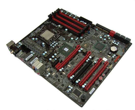
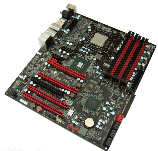
EVGA's Classified X58 motherboard has been a centerpiece of X58 discussions in various forums since the start of 2009. We managed to get an engineering sample board a few weeks ago and have some initial overclocking tests to show today. Let's take a quick look at the current layout and features before we have a look at a few early benchmark runs.


Our board arrived before EVGA finalized the stock cooling design, so we have had to resort to using third party solutions to cool areas of the board for these initial test runs. We are waiting on a retail board from EVGA before we comment on thermal performance and power consumption.
Hardware wise, EVGA added NVIDIA's NF200 into the mix that allows four x16 electrical interface PCI-E slots. As many of you already know, the NF200 is a PCI-E 2.0 x16 bridge-chip solution, which does add extra latency to the data transfer process. However, that's not a huge issue in the overall package.
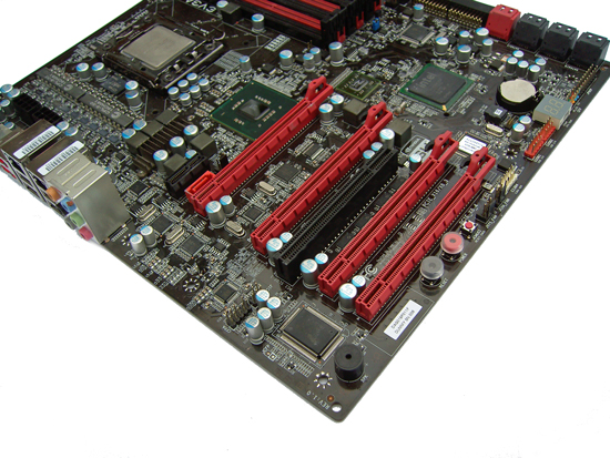
This board is set to become EVGA's flagship board by offering a slew of extreme overclocking friendly features. This holds true for the 10-phase Volterra CPU power, 3-phase memory power, and 3-phase VTT designs to onboard jumpers that override cold boot quirks for LN2 cooling. The product focus is squarely aimed at multi-GPU enthusiasts and those that benchmark more for competition than fun. The slot configuration allows running three dual slot GPUs and a single slot PhysX card or other PCI-E peripheral. A PCI-E x1 slot is available for audio duties, even if the GPU slots are completely loaded.
This board is clearly for those with deep, deep pockets. The launch price is expected to be around $400~$450, putting it off the radar for most. EVGA provides a plug-in remote PCB, supporting power, reset, CMOS clear, a hex POST code LED display, on-the-fly VCore adjustment, and PCI-E disable jumpers. The remote buttons come in handy when benchmarking the board out of a PC case, especially when the lowest PCI-E slot is occupied.
A new addition that EVGA just completed for the final retail board is the presence of an onboard ROM that can store memory SPD files. The user can select at BIOS POST to override the memory module base SPD. EVGA has developed an OS software tool that allows users to interchange SPDs with one another if a particular SPD file known to offer superlative performance for a memory chip/PCB combination is available. Our test board does not contain this technology, so we will have to wait for the arrival of our retail board to test this unique feature.
We have been throwing everything we can at the board using the latest test BIOS. So far, things have been smooth during the test process, mainly because the EVGA X58 SLI board's launch has provided insight to the EVGA team and us in getting this board up and operating quickly. Peripheral compatibility has been excellent on this board. We have not discovered a single device that was not recognized or refused to work properly. S3 resume states have worked for us all the way up to 215 BCLK (as far as we tested to date), which cures a problem on the X58 SLI board.
Unfortunately, we still do not have an official release date from EVGA, but we expect it sometime in March (subject to change, obviously). At stock speeds, this board offers similar performance to other X58 motherboards in a variety of applications and games. Our short preview today will cover SLI gaming performance to see if the NF200 is a handicap and a few overclocking results using subzero and water-cooling, which is relevant as this board is targeted at the competitive overclocking crowd.
We are also providing a descriptive analysis of the BIOS overclocking options and how they work not only on this board but also on the X58 platform in general. We will follow up with a revised BIOS guide when the board launches. In the meantime, let's take a quick look at our results today.
Test Setup
| EVGA X58 Classified | |
| Market Segment | Enthusiast and Extreme Benchmarking |
| CPU Interface | LGA-1366 |
| CPU Support | LGA-1366 Nehalem i7 Series of Processors |
| Chipset | Intel X58 |
| BCLK Speeds | 133~500 MHz in 1MHz increments |
| DDR3 Memory Speed | 800, 1067, 1333, 1600, 1867, 2133, 2400, 2667, 2933 Frequency Ratios |
| Uncore Frequency | Full i7 Processor IMC multipliers supported, Options available as per CPU |
| PCIe Speeds | Auto, 100MHz - 140MHz in 1MHz increments |
| Core Voltage | Auto, 1.00V to 2.24V in 0.00625V increments |
| CPU Vdroop Compensation | Enabled, Disabled |
| CPU Clock Multiplier | Dependant on Processor, all available multipliers supported |
| DDR3 DRAM Voltage | Auto, 0.70V ~ 3.39V in 10mV increments, 1.50V standard |
| DRAM Timing Control | tCL, tRCD, tRP, tRAS, + 17 additional timings + Chipset Configuration |
| DRAM Command Rate | Auto, 1T, 2T |
| IOH Voltage | 1.10V - 1.875V in 25mV increments |
| ICH Voltage | Auto, 1.05V ~ 1.825V in 25mV increments |
| CPU VTT (Uncore) Voltage | Auto, 1.17V ~ 2.17V in 25mV increments |
| CPU PLL Voltage | Auto, 0.60V ~ 2.70V in 75mV increments, 1.80V Base |
| IOH PLL Vcore | Auto, 0.60V ~ 2.70V in 75mV increments, 1.80V Base |
| QPI PLL Vcore | Auto, 1.10V ~ 1.875V in 25mV increments, 1.10V Base |
| IOH/ICH Voltage | Auto, 1.50V ~ 2.275V in 25mV increments, 1.50V Base |
| NF200 Voltage | Auto, 0.70v~1.075V in 125mV increments, then 1.20V~2.70V in 25mV increments. 1.20V Base |
| Memory Slots | Six 240-pin DDR3 DIMM Slots Triple-Channel Configuration Regular Unbuffered DDR3 Memory to 12GB Total |
| Expansion Slots | 4 - PCIe 2.0 x16, Supports up to NVIDIA 3-way SLI Technology + PhysX 1 - PCIe (1.x) x1 1 - PCI Slot 2.2 |
| Onboard SATA/RAID | 6x SATA 3.0Gbps Ports - Intel ICH10R Hot Plug and NCQ Support; RAID 0, 1, 5 RAID 0+1 Support; Intel Matrix Technology Support |
| Onboard IDE Additional SATA | 2xJMicron JMB363 PATA Controller (up to 2 UDMA 133/100/66 devices) 1 External eSATA port + 3 Internal JMB363 SATA Ports |
| Onboard USB 2.0/IEEE-1394 | 10 USB 2.0 Ports - (8) I/O Panel, (2) via headers 1x 1394a Ports - (1) I/O Panel, (1) via header |
| Onboard LAN with Teaming | Dual Realtek RTL8111C PCIe Gigabit Ethernet Controllers |
| Onboard Audio | Realtek ALC 889 -8 Channel HD audio codec |
| Power Connectors | ATX 24-pin, Dual 8-pin ATX 12V |
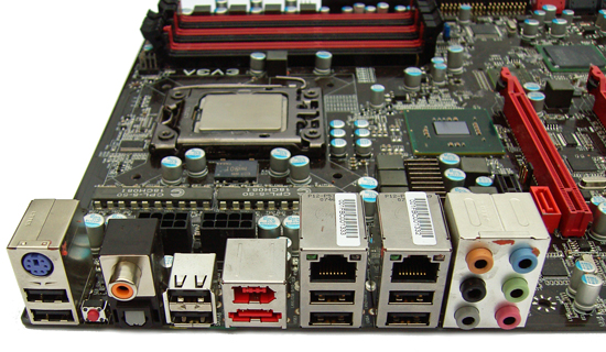
| I/O Panel | 1 x PS/2 Keyboard 1 x eSATA 1 x SPDIF - Coaxial Out, 1 x Toslink Optical Out 1 x IEEE 1394 2 x RJ45 6 X Audio Out 8 x USB 2.0/1.1 |
| Fan Headers | 1 CPU + 4 Additional Headers |
| Fan Control | Full Fan speed Control Via BIOS |
| BIOS Revisions Used | IX58S213 |
These are the current specifications and features planned for this board. We will go over these in detail once the retail board arrives and we can ensure nothing major has changed.
| Standard Test Bed Intel X58 Configuration |
|
| Processor | Intel Core i7 - 920 - 2.66GHz |
| RAM | Corsair TR3XGG1600C8D - 6GB DDR3-1600 G.Skill F3-12800CL9T-6GBNQ - 12GB DDR3 Patriot Viper PVT36G1600ELK - 12GB DDR3 |
| Hard Drive | Western Digital Caviar Black 1TB |
| Video Card | ASUS GTX-280 |
| System Platform Drivers | Intel - 9.1.0.1007 |
| Storage Drivers | Intel - 8.6.0.1007 |
| Video Drivers | NVIDIA - 182.06 |
| CPU Cooling | Vigor Monsoon III, 2X PA120.2 rads + DD Perta Top Pump for Water |
| Power Supply | Corsair - HX1000 |
| Optical Drives | Sony BDU-X10S, LG GGC-H20L |
| Case | ABS Canyon 695 |
| Motherboards | ASUS Rampage II Extreme - BIOS 1104 EVGA X58 Classified - BIOS IX58S213 EVGA X58 SLI - BIOS IX58SZ1N |
| Operating System | Windows Vista 64-bit Ultimate - SP1 |
| . | |
Our test setup today has a unique combination of cooling devices; otherwise, it is our standard test bed for the X58 products.
The Wet Stuff
We used water-cooling for our 24/7 stability runs. This is the same configuration we used when testing the EVGA X58 SLI. Using our i7-920 CPU, we were determined to find the maximum Prime95 stable overclock achievable on both boards by using the 19x multiplier (for BCLK addicts) and later the 21x multiplier to find the limits in raw CPU frequency. It is not surprising that both boards managed to overclock pretty close to one another considering our cooling system. The main differences between the boards are when we installed three GTX 280 cards along with a 6GB (3x2GB) memory configuration.
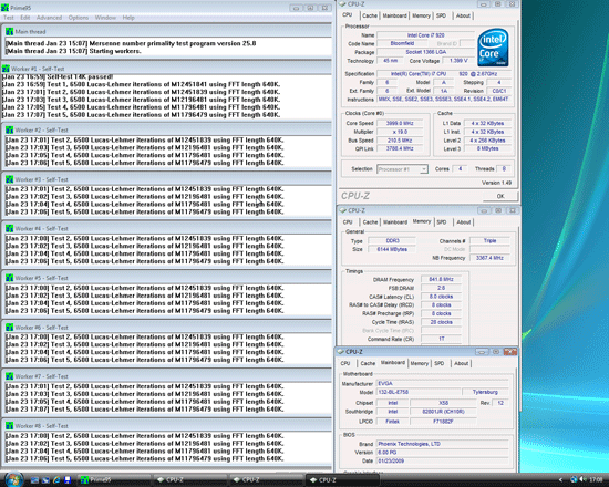

It's mostly academic, but the Classified pulls away by a small margin with 6GB of memory installed, although both boards will run 3x1GB at 215 BCLK. The EVGA X58 SLI board would not run any 8-thread CPU or 3D tests past 215 BCLK for us, while the Classified happily chugs along at 222 BCLK for 3DMark06 and 3DMark Vantage while retaining full stability in other applications. We could increase BCLK up to 227 for suicide runs in these particular benchmarks, but this would create stability problems in other programs.
The Cold Stuff
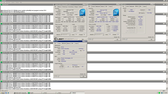
We used a test room with low ambient temperatures (16C) for the following benchmarks. We used water-cooling when the CPU was operating at 4.5GHz or below and Cascade cooling for benchmarks over this processor speed.
Conventional cooling methods will not show much gain in terms of how far you can push your CPU even with the X58 Classified board in your system. Thermal limitations of the Core i7 will surpass some of the benefits that the improved power circuitry of the Classified board will provide for overclocking users. What you will find is that the more robust nature of the X58 Classified becomes apparent when all slots are completely loaded in a heavily overclocked system.


Does the NF200 hurt performance?
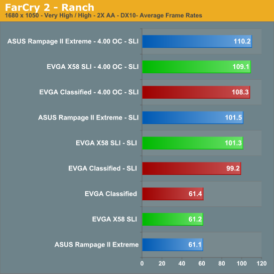
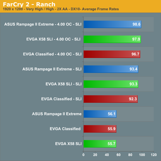
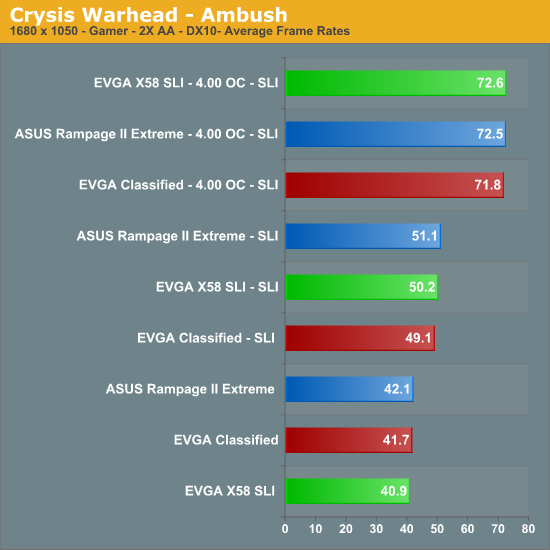
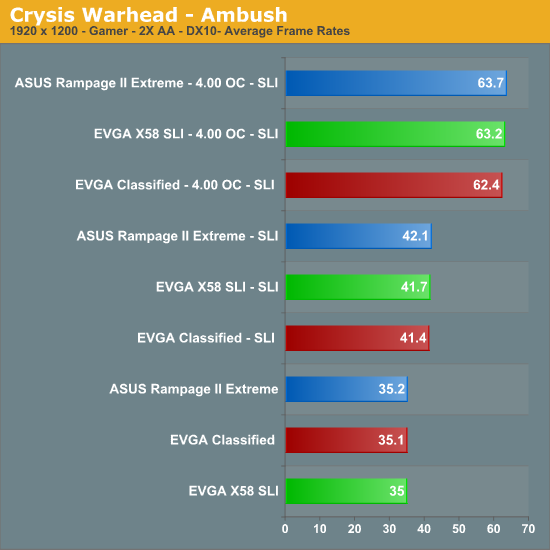
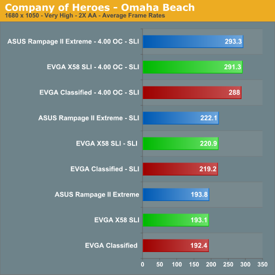
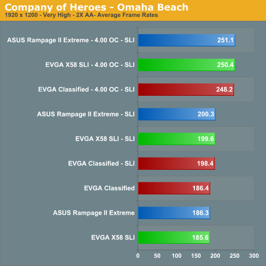
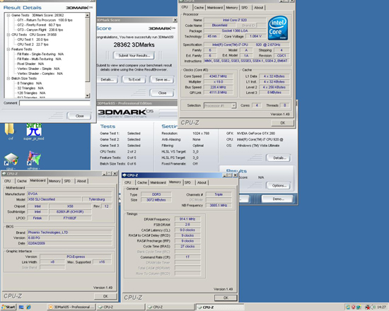
We are still testing SLI performance with the latest 182.06 driver release and the new BIOS we just received from EVGA. The performance penalties we are currently seeing with the NF200 equipped X58 Classified board average about 1%~3%. In other game benchmarks where we are not GPU limited, we have not noticed any performance differences between the boards.
BIOS Breakdown


Extreme Cooling
This function is only to be used when the CPU is cooled to subzero temperatures. Three settings are available depending upon the temperature range the CPU will be operating at for benchmarking. An alternative to this BIOS function is to move the onboard X-Cool jumper to pins 2-3, although the effects can be a little different to those offered in the BIOS. Our particular i7-920 CPU prefers the X-Cool jumper left at position 1-2, needing no change in the BIOS to reach the limits of thermal shutdown conditions. On the other hand, our i7-965XE processor prefers the X-Cool jumper at position 2-3. For us, we found we were able to boot and run our i7 processors another 10~15 degrees lower on the Classified than the cold boot limits imposed by other boards with these same CPUs.
PCI Express Frequency
This is useful when pushing the board beyond 222 BCLK. A setting of 102MHz will allow the BCLK frequency to be ramped past 222MHz using the E-LEET tuning program in the OS. For speeds past 230 BCLK, we used a setting of 114MHz. You can then boot into the OS at 220 BCLK and apply BCLK changes to take you directly to the desired CPU frequency. The use of high PCI-E bus frequencies does affect 3D stability however; too high and 3D benchmarks will lock mid-run. Settings over 117MHz or so give rise to SATA problems at times, so it's a case of edging up slowly and keeping your fingers crossed if you're going for an all out attempt at a maximum BCLK setting.
Profiles
Eight CMOS profile slots are available for saving your settings. Unfortunately, there is no way to name the saved profile for easy reference, which would have been a nice touch. Still, having these banks on hand makes it easy to re-apply previous settings when experimenting.
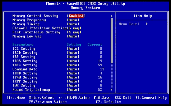
Memory Control Setting
Enabled: Allows manual control of Memory Frequency, Channel Interleave, and Rank Interleave.
Memory Frequency: This is the memory multiplier ratio to BCLK. It's self-explanatory based on the ratios and speeds listed. For those just starting on the i7 platform, a memory ratio of 10 (1333) and a base BCLK speed of 133 will result in a DDR3-1333 (10x133) memory speed as one example. As you clock up bus speeds, you will need to lower the memory ratio to keep your memory operating within specifications.
Memory Timing: EVGA has managed to find a number of memory controller presets based on the applied memory frequency. Our testing to date has shown no real performance gains between any of the presets other than stability, so we're veering towards calling this a signal timing offset rather than a latency adjustment. At stock processor speeds (133 BCLK), one can use the appropriate memory divider and MCH frequency setting to obtain the stock memory frequency. If you intend to experiment with individual MCH frequency settings then do note that if using the 1867 and 2133MHz presets that memory frequency must be close to the speed of the MCH preset. As an example:
BCLK 133MHz
Memory Multiplier 2:14
Uncore Multiplier 28
MCH "strap" = 1867
MemFreq =1867MHz
…POSTs
BCLK 133MHz
Memory Multiplier 2:10
Uncore Multiplier 20
MCH "strap" = 1867
MemFreq =1330MHz
…Fails to POST.
But:
BCLK 186MHz
Memory Multiplier 2:10
Uncore Multiplier 20
MCH "strap" = 1867
MemFreq =1860
…also will POST.
If memory frequency is below MCH "strap" frequency using the 1867 preset, then the minimum consistent boot up memory frequency is in the region of 1770MHz. Memory speeds over the MCH preset frequency are not as susceptible to non-post situations. The 1600MHz preset seems to be the most scalable and stable preset in our testing to date. Values in between the presets are catered for using the "by DRAM ratio" setting, which scales signal timing offsets in conjunction with memory frequency and BCLK.
Channel Interleave: Higher values divide memory blocks and spread contiguous portions of data across interleaved channels, thereby increasing potential read bandwidth as requests for data can be made to all interleaved channels in an overlapped manner. For benchmarking purposes when using three memory modules, a 4-way interleave may surpass the scoring performance of setting 6-way interleave depending on the benchmark and operating system used (32-bit vs. 64-bit). We did find however that a 6-way interleave was capable of a higher overall BCLK for Super PI 32M than using a 4-way interleave setting (unless of course you run single- or dual-channel and appropriate channel interleaving thus decreasing load upon the memory controller).
Rank Interleave: Interleaves physical ranks of memory so that a rank can be accessed while another is being refreshed. Performance gains again depend on the benchmark in question. For 24/7 systems using triple-channel memory configurations there is no advantage to setting this value below 4 while Channel Interleave should be left at 6 for best overall system performance.
The rest of the memory parameters pretty much default to optimum levels; moving away from these values can in some instances make matters worse in terms of system stability rather than performance. The current BIOS defaults are just about optimal for most overclocking. The highest performance advantage comes from changing the primary memory timings. There's little to no gain in fiddling with any of the secondary timing ranges, other than moving tRFC out to a value of 88 or more if running 12GB (6x2GB) of memory.
More BIOS Stuff
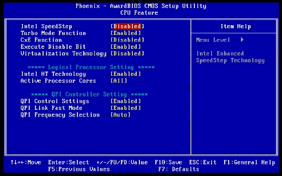
Intel SpeedStep: You can set this to Enabled for 24/7 overclocking. This setting will change the CPU multiplier dynamically depending on the processor load. A fine control of idle and full CPU load changes is available under the Vista OS in the power management option.
Turbo Mode: This locks the turbo state multiplier to "on" irrespective of system loads. When this function is active, an i7-920 processor will retain a 21X multiplier on all four physical and logical cores, regardless of the selected multiplier on the frequency/voltage control screen.
CxE Function: For maximum performance in score oriented benchmarking, set CxE to Disabled. The multiplier idle~ramp period, power saving, and cache flushing employed by some C-states increase L3 cache latency, which reduces scores in sensitive benchmarks. For 24/7 use there is no harm in activating SpeedStep and C1/C1E states to conserve a small amount of power during low CPU load and idle conditions. These functions should be used in conjunction with CPU power VDroop to maximize system stability. VDroop is a proverbial hornets' nest of often-misinformed opinions, so we will take a brief look at VDroop and where things can become a little nasty on certain motherboards.
C states and SpeedStep are reliant on stable power delivery to the CPU during multiplier step changes. Using VDroop with these two functions enabled ensures that CPU voltage delivery remains within specified tolerances. The Nehalem architecture is also able to dynamically alter VID values according to TDP (total power and current drawn). Hence, the inclusion of these functions on all i7 boards by default; it is how Intel designed these processors to work. Here is a very simple illustration of how this takes place.
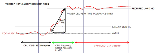
VID denotes applied VCore while VCC denotes the real-time voltage level; these are not to exact scale and are for illustrative purposes only.
The hold period of SpeedStep together with current and power load sensing by the processor allows VCC to settle before the maximum clock multiplier is enforced while VID tolerances remain observed. Voltage excursions that are drastically above or below VID not only can breach processor warranty tolerances with voltage spikes, but also give rise to increased power supply settling times as the PWM circuit feedback loop reacts to the initial power delivery error. During any form of oscillation, the power supply bandwidth is compromised for a small period of time at the resonating frequency. Ultimately, this increase in power line settling time can result in system instability and bring about the shortening of component lifespan. This is the exact reason that Intel set forth design tolerance margins that have to be observed to satisfy stock operation. It is up to the board manufacturers to include and satisfy these safety margins according to the capabilities of the circuits they choose.
Running a board with "no VDroop" under these types of condition may not only violate VID delivery guidelines but can also make the system unstable. Most PWM controllers are designed according to VRM 11.1 spec (they have to be at this point). The VDroop function is a pivotal part of the engineering and development process of these controllers, and configuring this function properly on a board maximizes the performance of the controller in question. It is for this reason that disabling VDroop on some boards may actually cause the voltage to rise when the processor goes into a load state. Disabling VDroop essentially changes the way the controller was designed to work. Custom implementations are obviously possible that surpass the Intel specification guidelines by a wide margin; however, VDroop and settling time are still important facets of high speed and high current operation.
In the following scenario (without VDroop), and with SpeedStep disabled, not only must the PWM controller stabilize VCC when the processor enters load state, but it also has to ramp VCore upwards to reach stable VID for the applied processor frequency - a double whammy for the PWM controller and output FETs. The CPU is overclocked and sitting at a static 4GHz speed regardless of idle or load conditions.
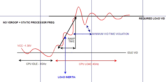
If VCC breaches the minimum processor frequency dependant VID for long enough the result is a system crash. The user will usually counter this effect by adding more voltage so that the idle VID is closer to the required load VID.
Fortunately, not all boards ramp VCC like this with VDroop disabled; if you happen to have one that does, enabling VDroop is not a bad idea at all. In the case of an overclocked processor, real-time software loads that modulate rapidly cause havoc for the PWM controller and FETs, as they fight the inertia of the load change and attempt to raise VID (VCC) while trying to stabilize the load line - not good. Compounding problems further is users seeing voltage fluctuations or a stable voltage as reported by onboard sensors contradicting any of the power delivery guidelines. Unfortunately, these sensing devices are only satisfactory for reporting a crude average voltage value and are nowhere near fast enough to show the real time VCC fluctuations that are occurring in the KHz ~MHz region. Simply put, voltages reported by the BIOS/sensor and software should not be trusted when trying to confirm the presence of voltage spikes on the VCC line.
With all this in mind, we always utilize VDroop for all of our "everyday" overclocking results. On this platform, we do so even when using LN2 cooling as the i7 architecture does not seem to need bucket loads of voltage to reach its full overclocking potential. Suitably engineered boards incorporate VDroop in a manner where VCC sags by around 0.07V under full load even when you apply 1.6V~1.7V in BIOS. So long as you know what the approximate full load VCore is, you can work around it without a problem. In fact, on boards that support dynamic VID changes when the processor is overclocked, we utilize this function for our 24/7 overclocks.
The Classified implementation of SpeedStep and C power states at the time of publication support dynamic VID at stock processor voltage (set to AUTO in BIOS). Once you move past the AUTO value for VCore, VID will remain at the BIOS applied voltage without changing dynamically at idle or load states. That means you don't quite get the IDLE VCore reduction when the processor is overclocked using any other voltage apart from AUTO in the BIOS. This is one of the compromises in having a board designed to push components as far as they will go by using a PWM controller geared for high current delivery far beyond stock speeds.
The 10-phase Volterra solution seems more than qualified to handle an overclocked Nehalem CPU's slew rate demands with its freakish over-engineered specifications. Using the "without VDroop" function on this board does not result in VID being raised during load conditions. However, for the sake of best power delivery and system stability, we still recommend you use VDroop for the best overclocking potential. No matter how good a controller is, VDroop will always help deliver the most stable power to the CPU.
Shocking BIOS options
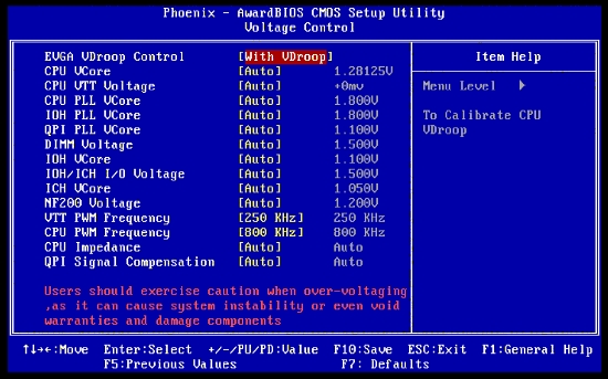
CPU VTT: Stock VTT voltage defaults to 1.17V or so. The scale runs in 10mv steps, allowing you to add or subtract from the base value. VTT voltage drives the integrated memory controller and the QPI link bus. This voltage will need to be increased as you increase memory frequency and increase BCLK (QPI frequency). Remember to keep this voltage within 0.5V of VDIMM to prevent damage to the integrated memory controller.
CPU PLL VCore: 1.8V base; we found no benefits to increasing this voltage for overclocking. Clean power to PLL circuits is essential for ensuring that external influences over the accuracy of clock signals is minimized. It seems EVGA have done a good job with regards to all PLL voltage rails on the Classified. In terms of overclocking headroom and PLL's, clean power always trumps more voltage, thus there's no need to tinker with these voltages to any great extent on this board, apart from perhaps QPI PLL. Even then, you'll probaby find the level of voltage required for maximum BCLK potential is far below what some other boards need to get the same clocks...
IOH PLL VCore: Input/Output Hub Phase Locked Loop voltage. The default voltage is 1.8V. For the most part this voltage can be left at stock unless chasing maximum QPI frequencies for benchmarking. For 24/7 use we recommend you stick with a maximum of 1.89V. Processors/IOHs needing more than 1.89V to remain stable are best run at a lower BCLK and higher CPU multiplier to bring them back into their comfort zone.
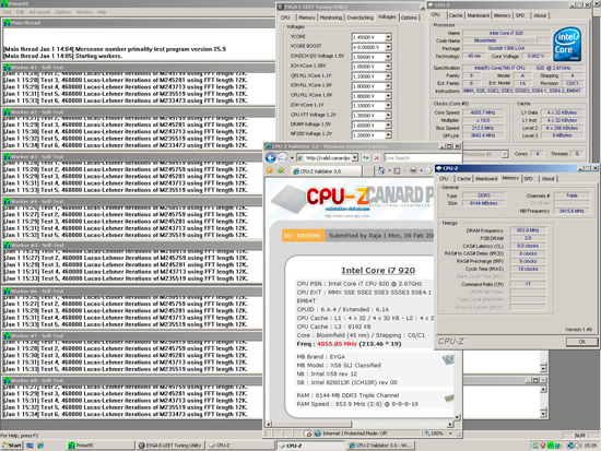
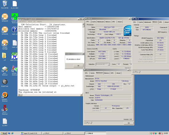
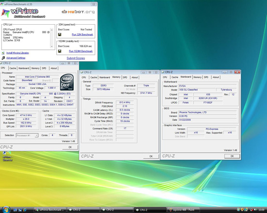
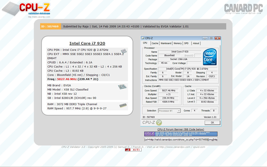
QPI PLL VCore: Quick Path Interconnect Phase Locked Loop voltage. For 24/7 overclocking this voltage can be left at stock in most instances. Again, if you need to use more it's probably wise to pull back a little on QPI frequency to a speed that requires no more than 1.2V. For benchmarking, we used 1.45V to reach 239 BCLK for a CPU-Z shot.
IOH VCore: Input/Output Hub voltage uses a 1.10V base. Stock values usually suffice for 24/7 overclocking even when using multiple graphics cards; we had no problems in reaching a stable 200 BCLK X20 for 4GHz CPU speed. For more extreme QPI frequencies this voltage will need to be increased. For 3D benchmarking past 220 BCLK we used 1.45V. We needed 1.50V to reach 239 BCLK. Values over 1.50V failed to POST or locked up in the OS; use only as much voltage as you need.
IOH/ICH I/O Voltage: IOH to Intel Southbridge termination voltage. We left this voltage at stock and did not see any overclocking improvements from increasing it on this board. Base value is 1.50V.
ICH VCore: 1.05V base voltage; again this voltage can be left at default.
NF200 Voltage: 1.2V stock. We left this voltage at stock for all overclocking.
VTT PWM Frequency: Changes the switching frequency of the VTT voltage line. Higher switching frequencies can help facilitate lower output ripple, and reduce overshoot while providing a higher frequency power bandwidth to the CPU. Setting a higher frequency with this BIOS option may improve overclocking headroom somewhat depending on the current drawn. For overclocking past 220 BCLK we generally used 490KHz; for speeds below this a 250KHz switching frequency worked fine for us and also reduces the heat output from the PWM FETs.
CPU PWM Frequency: CPU PWM (VCore supply) switching frequency. Stock is 800KHz, which is more than sufficient for 99% of overclocking. For subzero benchmarking you may wish to increase the switching frequency to see if it helps stability during heavy 8-thread CPU loads. The side effect in doing so is increased heat from the power FETs, although the temperature increase is quite small due to the use of a 10-phase power delivery circuit, especially as the FETs are indirectly cooled via the CPU power plane when the processor temperature is well into the negative region.
CPU Impedance: Sets the level of signal compensation for the QPI bus to the CPU. Higher QPI frequencies often demand a higher signal current, which means that compensation levels have to be changed in order to counter any signal line reflections caused by PCB traces and input impedance mismatches. The options available for this function are AUTO and Less. On the Classified, we found that QPI frequencies approaching 4GHz can benefit from a reduction in setting Less, even more so if the CPU frequency is well above 4.5GHz. Leave at AUTO for most 24/7 overclocking at BCLKs under 200MHz. For subzero cooling at high system speeds, set this value to Less to see if it helps with overclocking headroom.
QPI Compensation: Sets the level of signal compensation for the QPI bus to the IOH. There are three options for this function, those being AUTO, Less, and More. We found that IOH compensation is far more sensitive to changes in compensation values than the CPU. A setting of Less for high BCLKs and QPI frequencies almost always brings about additional system stability during benchmarking (at least in our experience). For all other purposes, this value can be left to AUTO.
Initial Thoughts
That is all we have for you at this time as the final retail release is rumored to be sometime in March with review samples arriving right beforehand. Users will need to gauge if they think spending an additional $100~$150 on the Classified is justified over excellent boards from ASUS, Gigabyte, DFI, and even EVGA in the $300 price range. This board will provide slightly higher QPI frequency abilities when overclocking with air- or water-based cooling solutions. It also has the ability to handle high capacitive loads (slots loaded completely) with ease. So far, the NF200 bridge chip has not been an adverse liability on graphics performance. Yes, there is a slight latency penalty, but it is not noticeable in most conditions.
For the ever demanding benchmarking community, you'll need to find a CPU that can take advantage of the 600W peak power this board can deliver. 8-thread CPU tests over 5GHz CPU speeds draw in excess of 400W peaks on this platform. Thus far, it's been hard to divide the various X58 boards in our labs into certain overclocking categories because there are very few "pre-screened" processors available from Intel that allow both high QPI and core speeds under chilled conditions. Our various retail processors do not fall into this category, although we have a couple of excellent processors for air- or water-cooling. However, they are not the same when run at subzero temperatures as some of the processors in the hands of the more fanatical benchmarking personnel found at various forums.
Below 4.5GHz, most of the X58 motherboards available are usually not a limiting factor. Perhaps we'll have to wait until the release of the upcoming D0 processor stepping before we can really start to see a gap between i7 motherboard capabilities in the 4GHz~4.5GHz range. EVGA's own results with higher quality processors have the board running 8-thread CPU tests at over 5GHz with an SLI configuration, so the potential is certainly there on this board.
We have found the X58 Classified to be the easiest board to use for subzero cooling. All of the other boards we have (ASUS, Gigabyte, Foxconn, and DFI) seem to present us with earlier cold boot limits, memory limits, and/or power up limits, which combine to make benchmarking at subzero temperatures very tricky.
The Classified's slot layout will appeal to those that run multiple graphics cards and still need room for a RAID controller or sound card. Most of the users we have spoken with over the past few weeks are weighing these types of options. Testing to date has indicated a multitude of peripherals work fine on this early sample with the current BIOS, so one would hope that retail release continues or betters this state of affairs.
If money is no object, the X58 Classified and its overclocking features make this board the new king of the hill. There is nothing on the horizon quite like it or as robust in no-nonsense power delivery for high processor clocks (even in early production form). With a high launch price, estimated to be in the $400~$450 region, EVGA knows they cannot afford any slip ups and rightly so.


