Original Link: https://www.anandtech.com/show/2484
ASUS Striker II Formula under the Microscope
by Rajinder Gill on March 19, 2008 4:00 AM EST- Posted in
- Motherboards
As SLI is only available on NVIDIA chipsets, users who are inclined to adopt multi-GPU systems are always intrigued to find out just what they can expect from NVIDIA's chipset when it's teamed up with a couple of their midrange or top-end graphics cards. (There's also Intel's Skulltrail platform and mobile offerings, of course, which add nForce 100 bridge chips to get around the NVIDIA chipset requirement.) Over the next week, we're going to pit EVGA's reference design 780i motherboard against the custom design ASUS ROG board known as the Striker II Formula to see which is the better overall solution, or do they each perform well in certain usage scenarios? That's what we'll find out.
Things are certainly becoming interesting within the multi-GPU market, even with SLI licensing restrictions in place. There is something of a challenge to multi-GPU capable motherboard solutions, as both ATI and NVIDIA have dual-GPU graphics cards available now. This will provide users with flexibility of choice, allowing the use of virtually any current PCI-E motherboard/chipset whilst still enjoying a single card variant of SLI or CrossFire.
Much of the success of the dual-GPU cards rests upon comparative pricing and driver integration, just as it does with dual-card or even triple-card SLI. Our testing over the past few months has shown that there is definitely room for improvement when using any form of dual- or multi-GPU rendering in today's games. Having said that, even if we take driver level optimizations and multi-GPU frame rate gains into consideration, the demand for multi-GPU solutions is still apparent, further bolstered by games like Crysis, thus creating an avid interest in SLI capable platforms.
 |
If NVIDIA has managed to get the 780i chipset "right", it may well offer users a viable alternative to Intel's own DDR2 chipset solutions. That's quite a mammoth task, especially since NVIDIA continues to use a chipset bus architecture that allows for either synchronous or asynchronous overclocking of the processor and memory.
Naturally, users of the older NVIDIA 680i based motherboards have aired concerns of issues pertaining to Front Side Bus and Memory Bus related "holes". They would also like to know just how stable the new NVIDIA boards are when overclocked using quad-core processors. NVIDIA has been working to improve these aspects on their 780i product, and we aim to put this to the test today.
Overall system performance is often marred by the additional chipset latency offset required to run the memory bus and FSB asynchronously. As with Intel chipsets, there are rules that determine just how tRD, memory dividers, and memory CAS (Column Address Strobe) must align to assure that the data transfer between the memory bus and FSB can take place. Users who wish to delve deeper into the technicalities and mathematics of tRD and CAS are encouraged to read this article. Although we are dealing with a different topology here, the concept of data transfer and timing is essentially the same, though additional delays and rules apply when both buses are out of sync with each other.
As there are so many similarities between the 680i and 780i, we'd expect and hope that some of the experience gained over the past 18 months by both NVIDIA and ASUS using the 680i chipset will carry through to the 780i motherboards. Moreover, what does opting for the custom solution from ASUS get you for the extra expenditure over the reference design? Let's take a first look at the ASUS Striker II Formula.
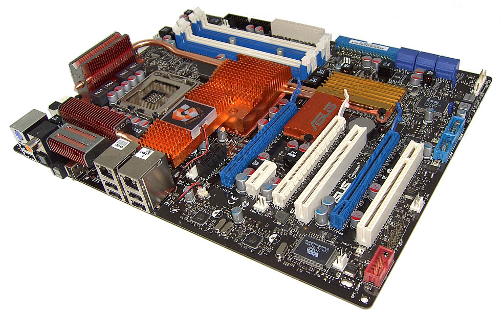
Board Layout and Features - ASUS Striker II Formula
 |
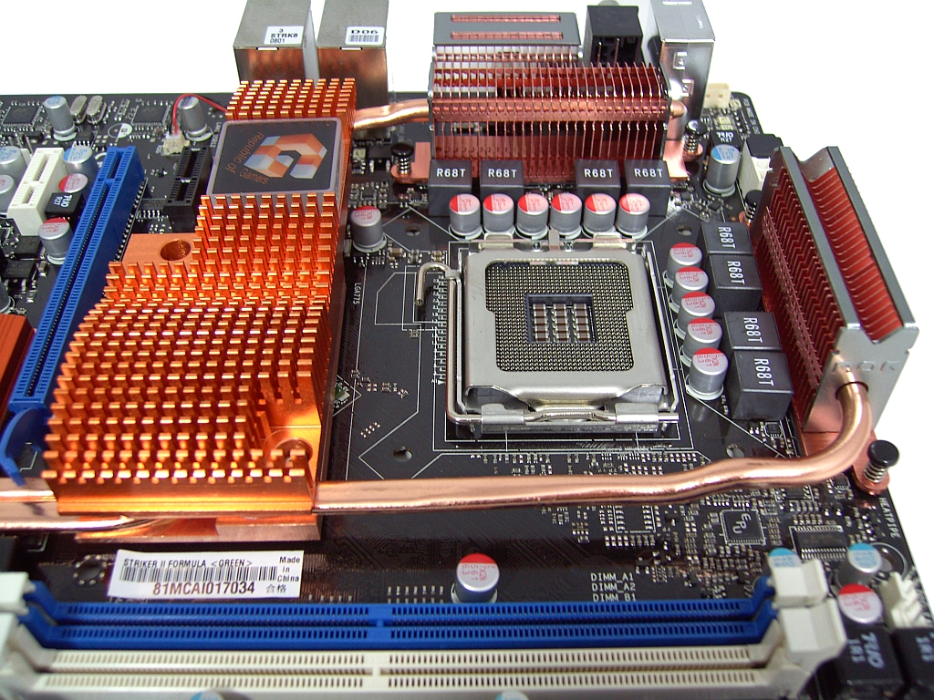 |
ASUS sticks with the tried and tested 8-phase CPU power circuit they have used for the past two years along with the regular array of heatsinks and heatpipes. Most air-cooling solutions should fit fine, though access to thumbscrews will be a little tight for coolers like the Tuniq Tower. The EPS 12V connector is at the top corner of the board. The CPU fan header is near the memory slots in the lower right corner of the picture. Seven system fan headers are located across the board to provide a variety of locations for attaching fans. Fan control is offered in the BIOS and via ASUS' own software, though the level of customization does not match that of abit's µGuru utility.
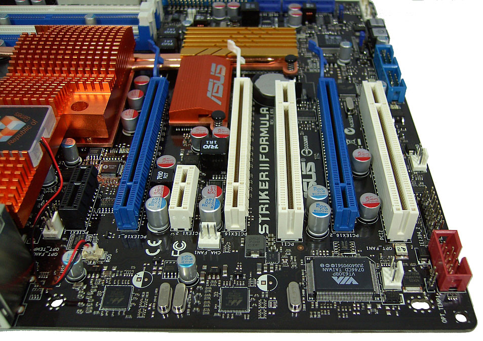 |
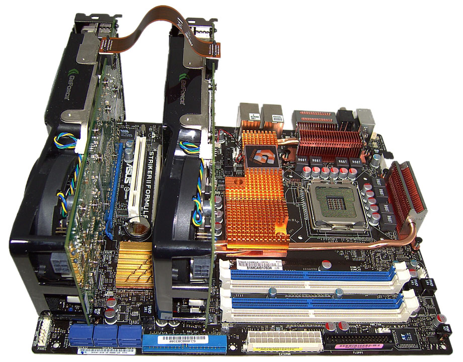
The PCI-E 2.0 compatible slots are far enough apart to allow a third graphics card to be used in the white PCI-E 1.1 x16 slot. The supplied Supreme FX II soundcard uses the black PCI-E x1 connector above the top PEG slot. Using dual graphics cards allows the use of the central PCI slot. When three air-cooled graphics cards are used, all other expansion slots (apart from the soundcard connector) are blocked.
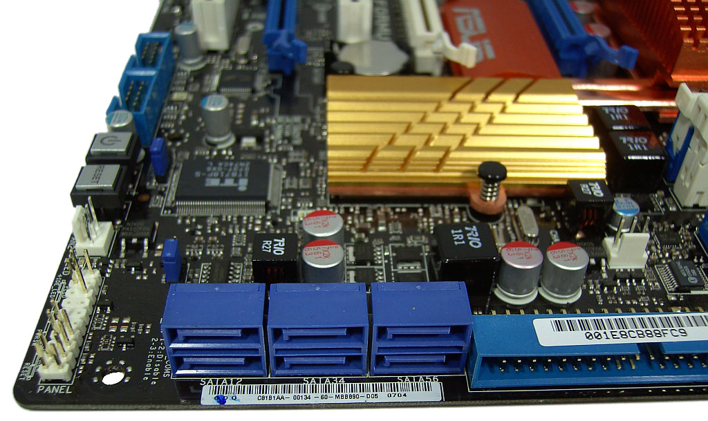 |
Six 3Gbps SATA ports capable of RAID 0, 1, 0+1, 5 and JBOD arrays are located at the edge of the board. The IDE connector is placed to the right of the SATA ports and has enough clearance from the PEG slots to allow access at all times. Power and reset buttons are at the lower edge of the board, for users who run open testbeds.
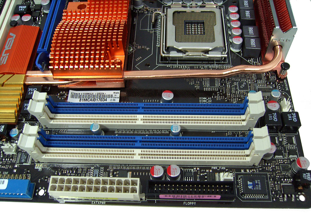 |
The ATX 12V connector is adjacent to the memory slots, with the 3.5" floppy connector placed to its right. Interestingly enough ASUS has employed a 2-phase memory power circuit using the low RDS MOSFETs we often see on their DDR3-based motherboards. This should allow extra overhead when using double density modules for 8GB memory overclocking - we will test this in a few pages.
Specifications - ASUS Striker II Formula
| ASUS R.O.G. Striker II Formula | |
| Market Segment | Gamer /Performance |
| CPU Interface | Socket T (LGA-775) |
| CPU Support | LGA775-based Core2 Duo, Core2 Extreme, or Core2 Quad recommended, including next-generation 45nm compatibility (06/05B/05A processors) |
| Chipset | NVIDIA nForce 780i SLI |
| CPU Clock Multiplier | 6x ~ 11x, downward adjustable for Core2, upward to 31x for Extreme, half-multiplier support for 45nm processors |
| FSB Speeds | Auto, 533-2000 (divide by 4) in 1 MHz Increments |
| System Bus Speeds | 1333/1066/800 MHz |
| DDR2 Memory Dividers | Sync Mode, 2:1, 5:4, 3:2, 1:1 and Multiple Async Dividers |
| FSB Strap | Automatic TRD adjustments based upon FSB speeds |
| PCIe Speeds | Auto, 100MHz ~ 200MHz in 1Mhz increments |
| PCI Speeds | Locked at 33.33MHz |
| DRAM Voltage | Auto, 1.80V ~ 3.40V in 0.02V increments, 1.80V standard |
| DRAM Timing Control | Auto, Manual - DRAM Timing Options (tCL, tRCD, tRP, tRAS, tRFC + 7 subtiming settings) |
| DRAM Command Rate | Auto, 1T, 2T |
| Core Voltage | Auto, 1.10000 to 1.81250 in 0.00625V increments |
| CPU PLL Voltage | Auto, 1.50 ~ 3.00v in 0.02V increments, 1.50V standard |
| FSB Termination Voltage | Auto, 1.20V to 1.70V in 0.02V increments, 1.20V standard |
| North Bridge Voltage | Auto, 1.20V ~ 3.00V in 0.02V increments, 1.20v standard |
| South Bridge Voltage | Auto, 1.50V ~ 1.85V in 0.05V increments, 1.50V standard |
| 1.2V HT Voltage | Auto, 1.20V ~ 1.95V in 0.05V increments, 1.50V standard |
| Bridge Core Voltage | Auto, 1.20V ~ 1.55V in 0.05V increments, 1.20V standard |
| Loadline Calibration | Enabled, Disabled |
| CPU Voltage Reference | Auto, Default ,+10mv ~ +160mv in 10 mv steps. -05mv ~ -315mv in 0.05mv steps |
| NB Voltage Reference | Auto, Default ,+10mv ~ +160mv in 10 mv steps. -05mv ~ -315mv in 0.05mv steps |
| Memory Slots | Four
240-pin DDR2 DIMM Slots Dual-Channel Configuration Regular Unbuffered, non-ECC DDR2 Memory to 8GB Total |
| Expansion Slots | 2
- PCIe 2.0 x16, SLI support 1 - PCIe (16x) x1, 1 PCIe X1 Slot for Supreme FX II Audio Card 2 - PCI Slot 2.2 |
| Onboard SATA RAID | 6 SATA 3Gbps Ports |
| Onboard IDE (PATA) | 1 x UltraDMA 133/100/66/33 |
| Onboard USB 2.0/IEEE-1394 | 10 USB 2.0 Ports - 6 On Rear I/O Panel - 4 Onboard
Connectors 2 IEEE-1394(a) Ports - (1) I/O Panel, (1) via Header |
| Onboard LAN (with Teaming) | Dual Gigabit LAN |
| Supreme FX II Audio Card | ADI 1988B - 8-channel HD Audio CODEC |
| Power Connectors | ATX 24-pin, 8-pin ATX 12V |
| I/O Panel | 1 x PS/2 Keyboard 2 x SPDIF - (1) Optical Out, (1) Coaxial Out 1 x IEEE-1394a 2 x RJ-45 (LAN) 6 x USB 2.0/1.1 1 Clear CMOS Switch |
| Fan Headers | 8 - (1) CPU, (1) Power, (3) Chassis, (3) Optional/Misc. |
| Fan Control | CPU and Chassis Fan Control via BIOS/Extreme Tweaker, PC Probe II monitoring |
| Thermal Sensor Headers | 3 Onboard Thermal Sensor Headers for Temperature Monitoring |
| BIOS Revision | 1001, 1101 |
Over a year ago, the NVIDIA 680i reference board gave the Striker Extreme 680i a run for its money. This time, ASUS has refined the power delivery circuitry to key areas of the Striker II Formula motherboard (memory and chipset power), giving it an apparent technical edge.
At present, online pricing of the Striker II places the board around the $300 mark, while the EVGA 780i A1 boards are priced at $259 direct from the EVGA site or around $230 at other online vendors. We have tested both boards in the labs and initial comparisons do show a marked difference in component and engineering choices between boards. The ASUS motherboard uses better components all around (something you would expect at the price). The question is whether these changes will justify the additional expenditure to the consumer.
Ultimately, we feel that the choices are going to come down to a couple of things. While the NVIDIA reference boards generally have the upper hand for BIOS base-code fixes (these eventually filter down into the non-reference boards), the rest will be determined by how hard you intend to push each board for overclocking and if you get a return for the extra ~$70 that the Striker II costs over its EVGA counterpart.
Making a decisive judgment call on overall overclocking potential is not easy though. The NVIDIA chipsets have shown remarkable variance in overclocking headroom from board to board in the past. A disparity as large as 25MHz FSB between boards of the same model is not unheard of between brands. In order to keep this variance to a minimum, ASUS screens the SPP units for their R.O.G. boards to ensure the best chipsets are utilized.
At first glance, we would say that comparing dual-core overclocking with up to 4GB of memory is like splitting hairs, as both boards would appear to have sufficient engineering to cope with these kinds of loads. The big question will be over the much-publicized Penryn overclocking ability that hounded the NVIDIA 680i chipset motherboards. The change that threw 680i-based boards off guard was centered on lower processor reference voltage levels (known as GTL) for the 45nm Intel CPUs. The 65nm CPUs require a reference voltage in the range of 67% of VTT, while the 45nm process requires around 63-64% of VTT (termination voltage) to achieve stability. Changes like these require a component level rework on boards that lack EPROMs and/or the required divider networks onboard that can be switched via BIOS coding to offer fine voltage changes to GTL reference voltage levels.
A larger cache size for the 45nm processors (especially the quad-core processors) also places more of a capacitive load upon the chipset, requiring additional signaling drive, again something that just can't be added via a BIOS workaround if the hardware is not adequate. This is why the early 680i boards are not stable with the 45nm processors or even the 1333MHz FSB 65nm units. Essentially, we are still working with the same Northbridge (680i) with improved GTL reference value adjustments to give higher stable FSB speeds with Penryn processors.
We would like to think that 400FSB with a 45nm quad-core processor will keep NVIDIA's solution competitive with the overclocking ability of the Intel chipset based boards. Our primary aim to test this today is to strap a 4GB and 8GB memory load to a QX9650 processor and see how well the board will work for stressful loops of PCMark Vantage and games like Crysis.
These tests will be repeated on the EVGA 780i board over the coming week, with a full report and cross comparison of both boards. We had hoped to have the EVGA results today, but our board failed before we could complete our torturous overclocking routines. It appears we had a weak SPP as the board gradually failed to overclock our quad-core processor, and at the bitter end it refused to even run at stock speeds. We sent the board off for a quick burial, but not before a 21 water gun salute.
Testbed Setup
| ASUS
Striker II Formula Setup Standard/Overclocking/Benchmark Testbed |
|
| Processor | Intel E8500, 1333FSB 9X Multiplier, Intel QX9650
Quad CPU, 12MB Cache 1333FSB Unlocked multiplier - 9X Default |
| CPU Voltage | 1.200V ~ 1.450V |
| Cooling | Water cooling: Swiftech Apogee GTX, PA120.3 Rad, 3 X Laing DDC Ultra Petra Top pumps in series, 3x Panaflo 120mm Fans 7-10V |
| Power Supply | OCZ 1000W |
| Motherboards | ASUS Striker II Formula |
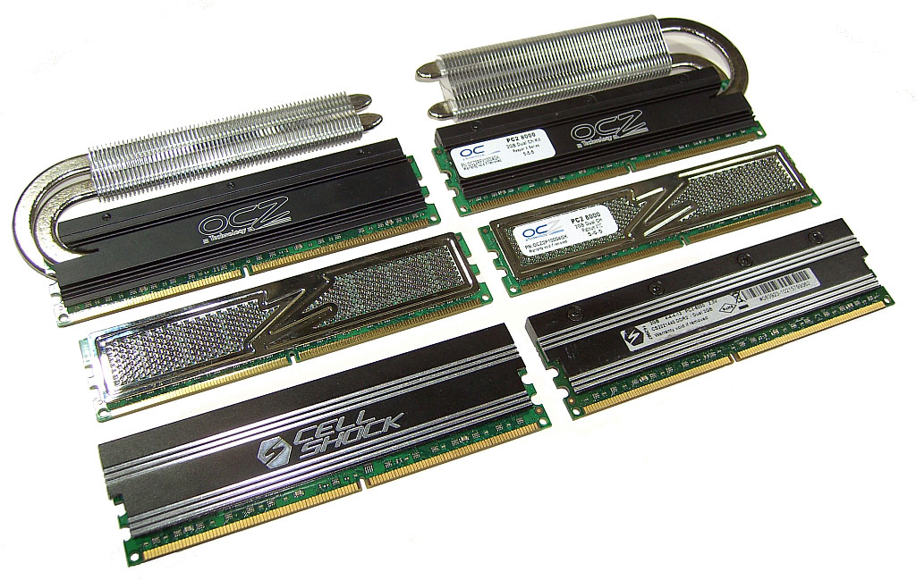
| Memory | OCZ Reaper-X 1000MHz 2X2GB kit, OCZ Platinum XTC PC2 8000 2x2GB, Cell Shock PC2 8000 4-4-4-12 2X1GB |
| Memory Settings | Various - as shown |
| Video Cards | ASUS 8800 GTS 512 G92 - Underclocked to match NVIDIA base clock levels for test comparison to 790/X48 chipset board scores |
| Video Drivers | 169.28Drivers (Vista 64-bit) |
| Hard Drive | Western Digital 7200RPM 250GB SATA 3/Gbps 16MB Buffer |
| Optical Drives | Plextor PX-B900A, Toshiba SD-H802A |
| Case | Lian Li -75 |
| BIOS | 1001, 1101 |
| Operating System | Vista 64-bit SP1 (4GB/8GB Memory), XP 32-bit SP3 (2GB Memory) |
| . | |
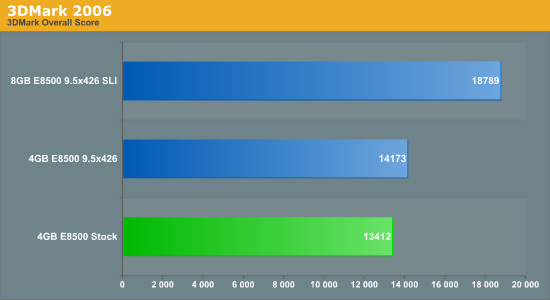
We performed 4GB and 8GB memory testing under the Vista 64-bit operating system using SP1. Our GPUs had to be underclocked to 650/1625/970 in order to match the GPU clock speeds used in the 790i launch article. This provides us with a broad range of scoring comparisons across a variety of boards for this review.
We tested in both single-GPU and SLI configurations with stock and overclocked processor speeds. Our primary concern in this review is to focus on absolute system stability, rather than outright benchmarking potential (though we may venture into testing this at a later date). We installed a new operating system image and software load between processor changes in order to eradicate any chances of driver or software conflicts.
We run each test five times and throw out the high and low scores and average the remaining three scores for our comparisons. We focused primarily on PCMark Vantage to represent a real-world type of system load that most of us subject our PCs to on a daily basis. Gaming tests use on Crysis, Unreal Tournament 3, and Company of Heroes. All three of these titles utilize different gaming engines, each representing a varying load to the entire system. We also crosschecked stability with OCCT's brutal CPU and memory tests.
PCMark vantage proved to be the most stressful test for our systems to pass; we had instances where the full two hour test of OCCT 2.01 passed, but PCMark Vantage would fail the gaming test repeatedly within a few seconds of launch. This is mainly because stress tests like Prime95 and OCCT do not stress the PCI-E bus, so we can only claim a form of 2D stability with this test at best. A broad suite of tests must be run to ensure any form of system stability for an everyday personal computer system. Component choices and variance in MCPs (chipsets) and other items will determine how close user boards will come to our overclocked results today; some boards may achieve more and others less.
We selected a few memory kits from our labs that represent the more popular current purchasing choices, coupled with one of the best 2x1GB performance kits from Cell Shock for a short test of Windows XP SP3 and stability/performance when running these modules. OCZ supplied the 2x2GB kits for our 8GB stress testing. Although this is not regarded as an everyday configuration, such a heavy load ensures that the stability of the board is tested to the fullest extent. 2x2GB modules are certainly all the rage at present with very aggressive pricing, to the point that we think 4GB should be a standard configuration for most systems, especially those running Vista.
We have grown quite fond of these kits in the labs; they operate up to DDR2-1000 speeds with very low levels of voltage, making for a cool running system with ample data manipulation potential. OCZ has also licensed a software tool called SPD-Z for flashing the SPD of these modules with performance related timing changes should the need arise on newer motherboards. Also, newer performance oriented 2GB modules from the likes of OCZ, G.Skill, and others are starting to hit the market that will approach DDR2-1200+ speeds that we will be testing shortly.
 |
Performance Results
| PCMark Vantage 64-Bit Performance Suite | |||
| 4GB Stock E8500 | 4GB E8500 426x9.5 | 8GB E8500 8.5x475 | |
| PCMark Score | 4867 | 5594 | 5822 |
| Memory Score | 4066 | 4546 | 4593 |
| TV and Movies | 3377 | 3896 | 3768 |
| Gaming Score (non SLI) | 4644 | 6053 | 5942 |
| Music Score | 4579 | 4810 | 4889 |
| Communications Score | 5166 | 6561 | 6551 |
| Productivity Score | 4022 | 5540 | 5068 |
| Company of Heroes Performance | ||
| 4GB Stock E8500 | 8GB E8500 8.5x475 | |
| 1280x1024 SLI | 243.3 | 303.1 |
| 1900x1200 SLI | 200.9 | 220.0 |
| 1280x1024 1GPU | 185.0 | 192.5 |
| 1900x1200 1GPU | 121.0 | 120.2 |
| Crysis High Quality Performance | ||
| 4GB Stock E8500 | 8GB E8500 8.5x475 | |
| 1280x1024 SLI | 49.64 | 62.19 |
| 1900x1200 SLI | 44.33 | 53.55 |
| 1280x1024 1GPU | 50.68 | 58.92 |
| 1900x1200 1GPU | 40.46 | 42.80 |
| Unreal Tournament 3 Performance | ||
| 4GB Stock E8500 | 8GB E8500 8.5x475 | |
| 1280x1024 SLI | 132.43 | 173.04 |
| 1900x1200 SLI | 126.44 | 155.01 |
| 1280x1024 1GPU | 131.67 | 151.52 |
| 1900x1200 1GPU | 100.89 | 103.63 |
Although the gaming frame rates are not quite on par with the 790i chipset under similar circumstances, the discrepancy is hardly enough to warrant dumping a lower cost SLI solution to favor the latest and greatest newcomer unless you absolutely must have the best performance.
To Sync or Not to Sync, that is the Question
One thing that has remained fairly unique to the NVIDIA chipsets is their ability to run the memory bus and FSB asynchronously from one another. In truth, the chipset just selects the nearest available memory divider to what the user inputs into the BIOS memory speed option. Basically, NVIDIA employs a lot of memory dividers and this gives them what appears to be a lot more freedom for overclockers.
For asynchronous memory speeds to work properly, additional tRD offsets must be employed to ensure that bus-to-bus data transfers fall within the timing window set by CAS (Column Address Strobe), the applied divider, and tRD. The result of this is usually a performance penalty, which is especially apparent when there are fewer memory cycles to FSB cycles (using a "down" divider) within a given period. In short, a percentage of the FSB cycles will pass without any data transfer taking place, while the MCH has to wait for a memory cycle to become available. The diagrams below should help us visualize this taking place a little better.
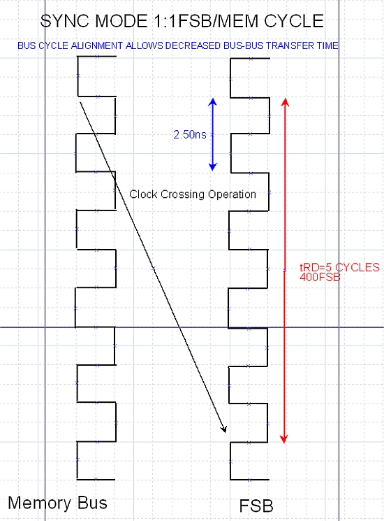
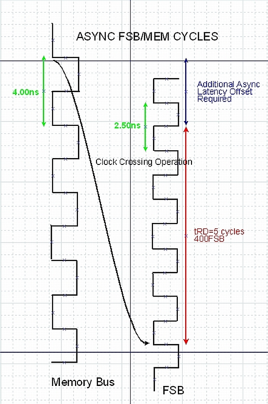
In sync mode, no additional tRD offsets are required, because a memory cycle is always available to the FSB to make a data acquisition. This makes it far easier to predict the rules of which CAS and tRD combinations will work together. However, when we expand this to include a myriad of divider combinations it's no surprise why many users have stumbled across "memory holes" on the 680i chipset that result in the motherboard not booting when certain combinations of timings are used. Users are again encouraged to read this article to obtain an understanding of tRD/memory divider and CAS relationships.
NVIDIA has worked very hard to eradicate these holes, and one of the key ways to employ a failsafe is to prohibit the manual adjustment of tRD via BIOS, rather opting for a static tRD value based upon the FSB speed selected by the end user. This way, the BIOS engineers can predict the possible permutations of memory timing and FSB speeds and ensure that the board is at least able to boot.
Moving on, the use of "up" dividers (where there are more memory cycles than FSB cycles in a give time frame), is not something we consider totally evil, as there are at least enough memory cycles to saturate the FSB with data. It is wise to generally aim for Sync mode wherever possible and at the most use an up divider if necessary. The Striker II generally tops out in Sync mode around 975MHz when overclocking. Of course, 2T timing rates are mandatory for 24/7 use when the memory bus is operating at this speed. 1T command rate is really only available for use below DDR2-850 speeds and requires judicious levels of VMCH to hold stability. 8GB overclocking is obviously bound by the rules of 2T command rates for operation at this time.
"Stable" Dual-core and Quad-core Overclocking Results
E8500 on Windows XP SP3 with Cell Shock's 2x1GB Kit
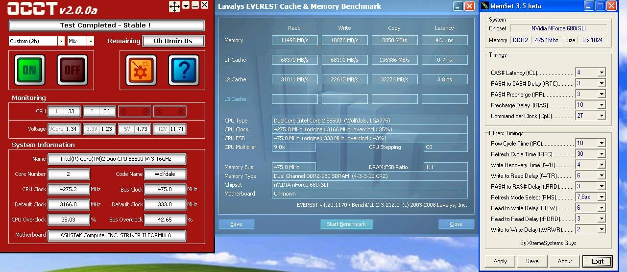 |
For dual-core processors running the XP operating system, the interesting zone is certainly around 475FSB running in sync mode. Don't be fooled by the memory speed at 950Mhz; remember 1:1 mode allows the most efficient form of data transfer via the MCH. For the Cell Shock modules - which use Micron's top D9GKX DDR2 bin - these speeds are a breeze. What's more, the speed comes at a voltage that the board and modules can easily operate at on a 24/7 basis.
We found that more than 2.15V on our modules was not necessary to hold these speeds 100% stable. The modules are certainly capable of a lot more, but it is nearly impossible to achieve it within warranty specifications. Of course YMMV (Your Mileage May Vary), but in general, if you have good DDR2 modules that are aggressively binned, this is the sweet-spot for operation on this board. We tested with a VMCH (Northbridge Voltage) at a mere 1.3V on our board to hold this setting steady. For us, this represents the greatest level of performance return per watt of energy expenditure.
E8500 with 8GB of OCZ's finest on Vista 64-bit
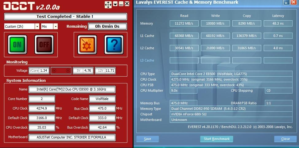 |
This was the shocker for us, using 8GB of OCZ memory with a dual-core E8500. The modules only required 1.95V to hold this speed, while VMCH was at 1.4V - both respectable. The read speeds are higher than we have managed on any Intel chipset using 8GB of memory. Sure, this is not mainstream yet, but we think that testing with 8GB offers an opportunity to check a board's stability much more than 2GB configurations. We have seen lower access latency on earlier Striker II BIOS releases; however, the stability was not there at these voltages. Things are a bit more sensible now and the board passed everything we threw at it - including multiple Crysis and PCMark Vantage test runs over the course of the last two weeks. Now the question is what happens when we replace the dual-core with a quad-core processor.
QX9650, 8GB, and Vista 64-bit equals trouble
This is where things enter the twilight zone. Finding stability at higher FSBs with quad-core CPUs can be quite a challenge on the 680i/780i chipset. On the back of our 8GB memory overclocking success using the E8500, we decided to go straight for the jugular and use 8GB of memory with the QX9650. Let's start with what we thought would be a stable configuration.
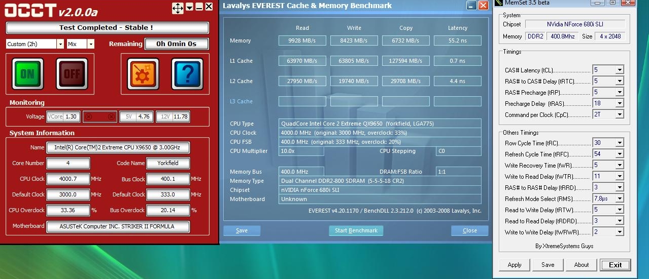 |
Although the transition in processors and configurations seems small when you look at the screenshots on the page, it does not show how long it took us to acquire this screenshot. Our initial attempts were all made by trying to dial in all the memory timings ourselves. Eventually we realized that tWTR needs to be very loose when using the QX9650 and set manually to 11 at the minimum. After repeated attempts, we let the board set the rest of the secondary timings via memory SPD. We stumbled across OCCT's base test with a pass, but Crysis failed in its first loop. PCMark Vantage also threw a "fit" when the 3D Gaming test began. We tried everything we could to get 3D stability but no amount of memory timing adjustments or component voltages brought us to the promised land of 3D stability.
The next step was to lower CPU multipliers and reduce CPU speed in order to coax a little more overhead from the Northbridge. Again we failed, all the way down to 3.2GHz when using 1600QFSB (400FSB). As the QX9650 has the advantage of an unlocked multiplier, we decided to use the 10x multi and a lower FSB speed. We even went down to using a 4GB configuration with the 2X2GB modules and found the same overall FSB wall. In the end we found that 3.5GHz with an FSB of 1400QFSB (350MHz) was the highest we could achieve and still pass PCMark Vantage. It seems that FSBs in the region of 400MHz have marginal stability with the quad-core processors when stressed with actual application benchmarks. We ran out of time to test with a 2GB configuration but will include this in part two when we take a close look at the abilities of EVGA's 780i board once we coax it back to life.
Initial Thoughts
Initial BIOS releases from ASUS were certainly a little rough around the edges, with each release completely changing how the board operates. The 1101 BIOS release is pretty much dead-on for dual-core CPU overclocking and general day-to-day use. During our time with the board, we were subjected to five different BIOS revisions, each with their own sweet-spots for performance and idiosyncrasies. Performance with the 1101 BIOS is generally good, and stability and peripheral device operation is excellent as we will see in the comparison article.
NVIDIA's 780i is on a par with the Intel X38/X48 DDR2 boards when it comes to dual-core CPU overclocking in the performance zone. ASUS has managed to supply clean power to the memory banks that allows us solid performance and 8GB memory overclocking potential, something we have not managed on other boards with the same settings.
It will be interesting to see how the reference boards measure up to the strengths of the Striker II Formula. For now, we would not hesitate to recommend this board for a dual-core SLI-based gaming system. Although 790i may be robbing this platform of the limelight, the real-world performance figures of both platforms are not enough to convince gamers that they need to make a jump over to the new DDR3-based chipset unless they have money burning in their pockets.
For the quad-core CPUs, we see the 780i coping with the 45nm Penryns in the same way we experienced when the 680i was first introduced to 65nm quad-core processors. As we expected, refinements to the GTL reference voltage circuitry has improved things a little, but the basic characteristics of the 680i SPP remain intact. The stable FSB limits of the 780i boards are still lower than we'd like - especially compared to Intel boards.
It's also interesting to note that the board behaves quite differently in its reboot cycles and failed overclock recovery when a quad-core CPU is used for testing. These effects generally begin to manifest as FSB speeds approach 400FSB, while speeds over this may require a CMOS reset to get the board up and running again. Then you can return to the prior settings before the overzealous overclocking attempt.
Our experiences using the EVGA 780i board so far have shown similar tendencies in certain ways, so the fault is down to the BIOS base code or the SPP itself. "Memory hole" issues are almost non-existent, with the Penryn quad-cores being the only ones to show any real flaws in the current BIOS. We still have some testing left to do, and our conclusion hinges upon the capabilities of the EVGA board when subjected to similar forms of testing. (The failure of the original board is naturally a concern already, however.) Of course, we are seeing the revised 750i and 650i boards hold their own in SLI performance in the midrange sector, so our final roundup of NVIDIA's current products for Intel owners should be interesting.


