Original Link: https://www.anandtech.com/show/2427
ASUS ROG Rampage Formula: Why we were wrong about the Intel X48
by Kris Boughton on January 25, 2008 4:30 AM EST- Posted in
- Motherboards
Every once in awhile, something comes along that is simply brilliant in its simplicity. For ASUS, that time could be now. ASUS plans to continue in their tradition of early adoption of new chipsets with a mid-February release of their upcoming Rampage Formula motherboard, a board that will make use of Intel's recently announced X48 Express chipset and DDR2 memory. Although DDR3 has been available for purchase for many months now, exceedingly low DDR2 prices have made purchasing 4GB or even 8GB of memory quite affordable - the latter still costing less than 2GB of good DDR3 memory. Coupled with the fact that the Rampage Formula provides a relatively easy upgrade path for current DDR2 owners, we can see why this board will be an attractive choice for anyone looking to build their next high-performance gaming system.
Like other recent offerings from ASUS, the Rampage Formula is part of the Republic of Gamers (ROG) line of motherboards, aimed squarely at the enthusiast looking to tune all levels of system control in order to extract every ounce of possible performance. We were a little surprised to see that ASUS seems to have needed very little engineering work in order to make use of Intel's higher-binned X48 chipset - the Rampage Formula and the currently available Maximus Formula (which uses the X38) share almost everything in common with the exception of the Northbridge. On one hand this makes sense, as the X48 is little more than an X38 binned for ultimate performance; on the other hand we would have liked to see a few additional improvements in component choices and layout.
Because of this, those that already own an X38 ASUS motherboard may find no compelling reason to upgrade. However, gamers ready for a complete system overhaul looking to build with the absolute best quality board should strongly consider the Rampage Formula. Compatibility was excellent with no real gripes to speak of - the board flawlessly made use of every CPU and memory kit we installed for testing. Coupled with one of Intel's new 45nm quad-core or dual-core CPUs and a pair of ATI 3000-series Radeon cards in CrossFire, this board provides a solid centerpiece for a formidable gaming rig.
We would be delinquent in not noting the impending release of the Rampage Formula's DDR3-based companion, the Rampage Extreme. We anxiously await our chance to bring you an early first-look at what it has to offer. We fully expect that it will best even the most refined X48/DDR2 board. Our experience has always been that the X38/X48 chipsets simply work better when teamed with DDR3 memory. For whatever reason, we find that for absolute ease of overclock and rock-solid stability nothing beats an X38/X48 DDR3 board. Unfortunately, DDR3 prices can be a rather large obstacle for some, especially when dealing with the higher speed bins.
For now, we are happy to report that our early dealings with the ASUS Rampage Formula have been extremely satisfying, especially considering the relatively short amount of time given to BIOS maturity. In fact, we feel there are no significant obstacles impeding the release of this board. Additionally, we must applaud ASUS for the industry-leading effort they have put forth in incorporating a few new settings into the BIOS that give the user the ability to easily unlock otherwise hidden memory performance with just a quick finger twitch.
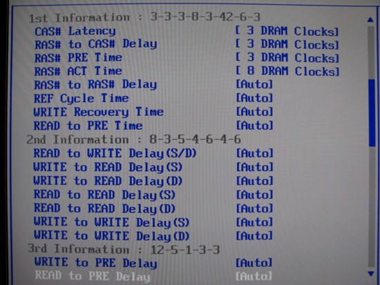
What are these settings you ask? Simply put, the ability to select a MCH Read Delay (tRD) from within the BIOS, as well as a means for adjusting the timing of each individual memory phase associated with the selected memory divider. You may know this setting by its more common name, often referred to as "Performance Level". While some motherboard makers have been making use of these settings for quite some time, never before has it been as de-obfuscated as it is today.
Hopefully we can finally say goodbye to the frustration of blindly adjusting these settings with the hopes of achieving the desired end goal - an accomplishment we can all appreciate. Our hopes are that other vendors follow suit and work quickly to update their offerings to provide this level of control in a similar manner. For those that are interested, we will touch on the performance improvements that can be seen as well as the other implications involved with making use of these settings a little later on.
With X48, the tier one giants - ASUS included - are gearing up for another round of lightning-fast motherboard releases. It appears as though they are now simply waiting on the green flag from Intel before they release these boards to the world. The fickle-free operation and high probability of success when overclocking that comes with teaming an Intel processor with an Intel chipset makes picking up an ASUS Rampage Formula an easy choice. One thing's for sure, ASUS is on a roll, and they don't appear to be slowing down for anyone.
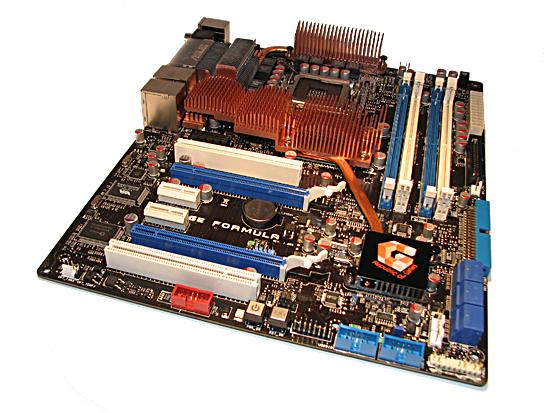
Board Layout, Features and Specifications
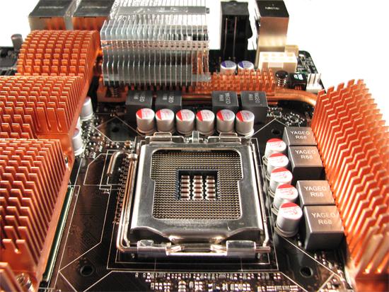
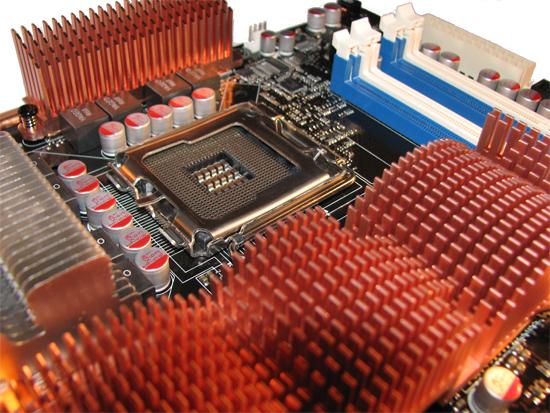
The ASUS Rampage Formula makes use of a beefy 8-phase PWM solution. The copper heatsink covering the MOSFETS is actually not thermally coupled to the Northbridge or the Southbridge as the cooling solution consists of two separate blocks. The hold-down mechanism for the X48's high quality heatsink is comprised of four tension screws attached to a backplate on the opposite side of the board. Besides changing the thermal paste ASUS utilized, we feel there is nothing that needs modification by the end user as long as overclocking aspirations are within reason.
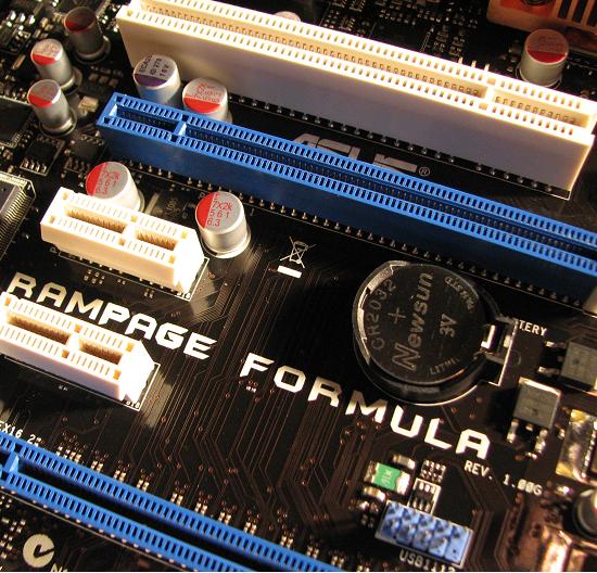
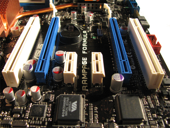
Two full x16 PCI-E 2.0 slots are available for official CrossFire support and the spacing is appropriate. We would have liked an additional PCI slot, for a total of three, instead of the three x1 PCI-E 1.x slots.
Six onboard SATA headers are on the right side of the board, each at 90 degree angles. This made inserting and removing cables easy, even with two full-length video cards installed.
One feature we particularly like is the volt-minder LEDs - one each for the CPU, Northbridge, Southbridge, and memory slots. Each can be one of three colors - green, yellow, or red - and they are useful for determining at a glance the approximate voltage being fed to each component. Green represents "safe" voltages, yellow is elevated (high), and red means "crazy high." Crazy high is just that too, as the board won't set the light red for the CPU voltage until it eclipses about 2.025V.
| ASUS R.O.G. Rampage Formula | |
| Market Segment | Gamer / Extreme Performance - $299.99 (estimated) |
| CPU Interface | Socket T (LGA-775) |
| CPU Support | LGA775-based Core2 Duo, Core2 Extreme, or Core2 Quad recommended, including next-generation 45nm compatibility (06/05B/05A processors) |
| Chipset | Intel X48 Northbridge (MCH) and ICH9R Southbridge |
| CPU Clock Multiplier | 6x ~ 11x, downward adjustable for Core2, upward to 31x for Extreme, half-multiplier support for 45nm processors |
| Front Side Bus Speeds | Auto, 200 ~ 800 in 1MHz increments |
| System Bus Speeds | 1600/1333/1066/800 (MHz) with Official DDR-1066 Support |
| DDR2 Memory Dividers | 1:1, 6:5, 5:4, 4:3, 3:2, 8:5, 5:3, and 2:1 (dependent upon strap setting) |
| FSB Strap | Auto, 200, 266, 333, 400 |
| PCIe Speeds | Auto, 100MHz ~ 180MHz |
| PCI Speeds | Locked at 33.33MHz |
| DRAM Voltage | Auto, 1.80V ~ 3.40V in 0.02V increments, 1.80V standard |
| DRAM CLK/CMD Skew CA/CB | Auto, Manual (Advance/Delay 50ps ~ 350ps in 50ps increments) |
| DRAM Timing Control | Auto, Manual - 20 DRAM Timing Options (tCL, tRCD, tRP, tRAS, tRFC + 15 sub-timings) |
| DRAM Command Rate | Auto, 1N, 2N |
| DRAM Static Read Control | Auto, Enabled, Disabled |
| Ai Clock Twister | Auto, Light, Moderate, Strong |
| Ai Transaction Booster | Auto, Manual |
| Common Performance Level | 1 ~ 31 (settings above 14 prevent POST) |
| CH A/B Phase Pull-In | Based on Memory Divider, All Phases Adjustable (Enabled/Disabled) |
| Core Voltage | Auto, 1.10000 to 1.60000 in 0.00625V increments then 0.05V increments |
| CPU PLL Voltage | Auto, 1.50 ~ 3.00v in 0.02V increments, 1.50V standard |
| FSB Termination Voltage | Auto, 1.20V to 2.00V in 0.02V increments, 1.20V standard |
| North Bridge Voltage | Auto, 1.25V ~ 1.85V in 0.02V increments, 1.25v standard |
| South Bridge Voltage | Auto, 1.050V ~ 1.225V in 0.025V increments, 1.050V standard |
| SB 1.5V Voltage | Auto, 1.50V ~ 2.05V in 0.05V increments, 1.50V standard |
| Loadline Calibration | Auto, Enabled, Disabled |
| CPU Voltage Reference | Auto, x0.63, x0.61, x0.59, x0.57 |
| NB Voltage Reference | Auto, x0.67, x0.63, x0.60, x0.57, x0.56, x0.53, x0.51, x0.49 |
| Memory Slots | Four 240-pin DDR2 DIMM Slots Dual-Channel Configuration Regular Unbuffered, non-ECC DDR2 Memory to 8GB Total |
| Expansion Slots | 2 - PCIe 2.0 x16, Supports ATI CrossFire
Technology 3 - PCIe (1.x) x1, (1) is Compatible with Add-in Audio Card 2 - PCI Slot 2.2 |
| Onboard SATA RAID | 6 SATA 3Gbps Ports - ICH9R (RAID 0, 1, 5, 10) |
| Onboard IDE (PATA) | JMicron JMB368 PATA Controller (up to two UDMA 133/100/66 devices) |
| Onboard USB 2.0/IEEE-1394 | 12 USB 2.0 Ports - (6) I/O Panel - (6) via
Headers 2 IEEE-1394(a) Ports - (1) I/O Panel, (1) via Header |
| Onboard LAN (with Teaming) | Realtek RTL8110SC - PCI Gigabit Ethernet
controller Marvell 88E8056 PCI Express Gigabit Ethernet controller |
| Onboard Audio | ADI 1988B - 8-channel HD Audio CODEC |
| Power Connectors | ATX 24-pin, 8-pin ATX 12V |
| I/O Panel | 1 x PS/2 Keyboard 2 x SPDIF - (1) Optical Out, (1) Coaxial Out 1 x IEEE-1394a 2 x RJ-45 (LAN) 6 x USB 2.0/1.1 1 Clear CMOS Switch |
| Fan Headers | 8 - (1) CPU, (1) Power, (3) Chassis, (3) Optional/Misc. |
| Fan Control | CPU and Chassis Fan Control via BIOS/Extreme Tweaker, PC Probe II monitoring |
| BIOS Revision | v0108 |
| Board Revision | 1.03G |
The ASUS Rampage Formula provides an impressive range of setting specifications. We would go so far as to say that more than a few of these are simply ridiculously high; however, there are sure to be a few people that require these options. A couple of the higher settings to pay attention to: CPU voltage well above 2.0V, CPU PLL voltage to 3.0V (sure to kill your chip super quick), FSB Termination voltage to around 2.0V, and DRAM voltages over 3.4V. While we certainly must commend ASUS on their fine range of control we also feel the need to strongly caution users when working with some of these settings. It's entirely possible to damage or destroy your chipset, CPU, or memory when moving to the extreme limits of these ranges; sometimes less is more.
As we have discussed before Loadline Calibration is best left disabled, especially when using the newer 45nm CPUs. Our testing has shown these settings induce power instabilities, even when using lower voltages. In addition, when enabled the option sometimes requires more CPU voltage than would otherwise be necessary, meaning increased power dissipation and higher temperatures.
Of note, the Rampage Formula allows for half-multiplier usage. This is particularly useful when working in the higher FSB ranges. Because all Core 2 Duo/Quad CPUs are downward unlocked, every half multiplier between the processor default value and 6 can be used, with the exception of 6.5x. For the Extreme processors, this limitation has been relaxed allowing for multipliers as high as 31x in half steps. Besides providing finer CPU frequency control, half-multipliers permit a wider choice of final multiplier/FSB combinations, which can help when choosing the best operating point for the processor and memory. Now that we have experienced what these new values have to offer, it will be hard to work with anything else.
As we pointed out before, "Ai Transaction Booster" is completely revamped for this board series. Setting this option to manual allows the user to take full control of the "Common Performance Level", meaning that all memory phases will baseline at the value as set. Each individual phase can then be "pulled-in" or left as is. "Pulling-in" a phase reduces just that phase's associated tRD value (performance level) by one. Like memory timings, lower values are tighter and thus provide better memory read performance and lower latencies. If all phases are pulled-in, this is the equivalent of selecting the next lower common performance level and performs identically to this new setting. Thus, pulling-in particular phases can allow the user to affect a minor performance improvement if selecting the next lower common performance level is not possible.
BIOS Screenshots and Interesting Settings
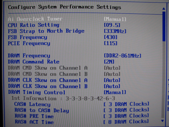
ASUS boards are known for their high level of customization and the Rampage Formula is no exception. The main menu that provides a majority of the options normally associated with overclocking is renamed "Extreme Tweaker", which we feel is entirely appropriate. Users can adjust everything from here, from bus speeds to voltages and memory timings to MCH parameters. Although a few options with indeterminate purposes still exist (for example, "Ai Clock Twister"), for the most part ASUS has done an excellent job in clearly labeling what each setting does.
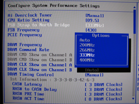
The ASUS Rampage Formula comes with official FSB1600 support, a feature attached to the use of the upcoming X48 chipset release. Those that want to use the next Intel Core 2 Extreme, the QX9770, will need to buy a board built around X48 if they want a platform validated for 400MHz FSB operation. We found the Rampage required no additional MCH voltage when running at this FSB setting.
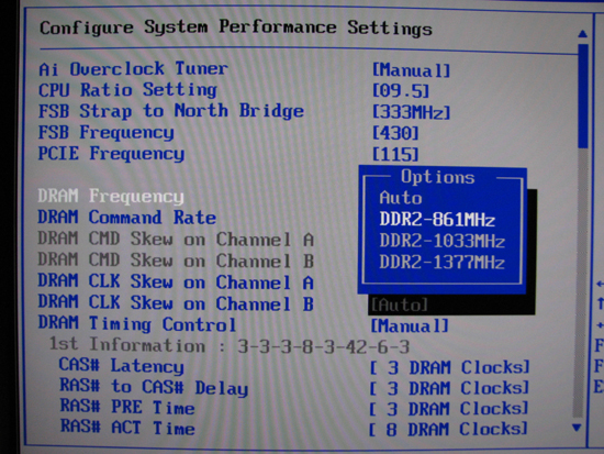
The standard compliment of DDR2 dividers is included in the Rampage Formula's BIOS. We will go into more detail about these later in the review. In any case, even with the fastest DDR2 available, we are not left wanting when it comes to options for pushing our memory.
The BIOS includes adjustment options for all primary memory timings - 20 in all. Most of the time a majority of these can be set to "Auto" - ASUS' tuning is already quite good. However, experienced users and memory experts alike will enjoy the expansive level of control allowed.
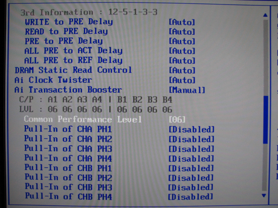
Here we can get a good look at what we consider the most significant change to the standard ASUS BIOS offering in years. "Common Performance Level", more correctly known as MCH Read Delay (tRD), allows the user to specifically establish a desired value, something that was not entirely possible in the past. Earlier versions of "Ai Transaction Booster" only allowed the user to apply an offset, which made controlling tRD difficult when the base value was unknown.
Additionally, each FSB bus cycle "phase" for each channel can be further manipulated. "CHA" and "CHB" refer to the two independent memory channels in a dual-channel memory configuration. Installing only one memory DIMM, or certain combinations of mismatched memory module pairings across all four expansion slots, results in the motherboard defaulting to single-channel operation; otherwise there are two memory channels in operation, which enhances overall system performance. The number of phases per channel depends on the memory divider in use (each channel will always have the same number of channels though) - a 3:2 memory divider has two phases, 4:3 has three, and 8:5 has five, for example. We will explore the theory behind this truth shortly.
Setting a single channel/phase "Pull-In" to enabled has the effect of lowering that particular phase's associated tRD value to one below the Common Performance Level (the "base" tRD). Leaving the setting disabled leaves the phase unadjusted, in which case it is the same as the base tRD. Much like memory timings, lower tRD values bring greater performance. As we will see, these settings primarily allow users to squeeze out any unclaimed performance benefit possible with the current tRD when the next "lower" Common Performance Level is unachievable. Do not feel as though you need to understand what all of this means right now, as we will cover all of this and much more in excruciating detail soon enough.
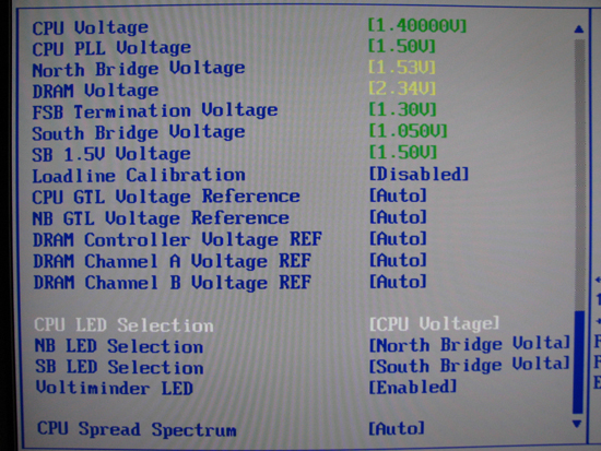
With no less than seven onboard voltage adjustments, the Rampage Formula is a tweaker's dream come true. Because ASUS motherboards do make a habit of "adjusting" some of these values automatically at times, we recommend you manually set all voltages to the bottom of their ranges unless otherwise required. This best practice just makes good sense and ensures nothing receives more voltage than intended by the user. Again, we must also strongly caution against the use of "Loadline Calibration." We recommend you leave this option disabled, especially when installing a 45nm CPU.
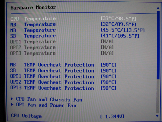
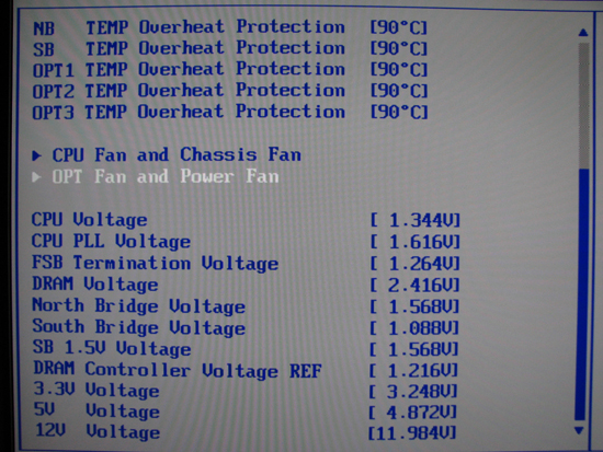
ASUS' implementation of their in-BIOS hardware monitor is extremely informative. You can simultaneously check temperatures for the CPU, motherboard (PWM), Northbridge (NB), and Southbridge (SB) as well as quickly review the effect that prior voltage adjustments had on actual voltage levels. Although we found most reported voltages were fairly accurate, obtaining the most precise readings possible still requires the use of a digital multimeter (DMM).
Regarding voltages, we found two concerns worth mentioning. Firstly, the reported CPU PLL voltage appears to be non-functional as it always reads the same, regardless of setting. Second, like many other ASUS offerings the motherboard consistently overvolts the memory by 0.08 ~ 0.10V. We do not see any real problem with this, as long as the user is aware it's happening.
The Basics of Strap Selections, Dividers and Derived Memory Speeds
We have discussed MCH Read Delay (tRD) and its effects on memory read performance before. About a year ago, this particular setting allowed some vendors to design boards that seemed to outperform competing companies' products consistently on a clock-for-clock basis. This was around the time that the enthusiast community first realized the importance of "straps". Some found that by setting a lower strap while running an equivalent Front Side Bus (FSB) that they were able to achieve better performance, higher frame rates, and better benchmark completion times all without the help of any additional tuning.
For those that are unfamiliar with what we mean by strap, consider the following example. Suppose you have two different CPUs, each with a different default FSB, as is the case with first-generation Core 2 processors (266MHz) and current 45nm Core 2 processors (333MHz). If you were to install these processors in identical systems each would be capable of running the same memory speeds (at least DDR2-667 and DDR2-800), regardless of the processor's default FSB. For the 266MHz default FSB processor, this would require a 5:4 and 3:2 divider respectively, while the 333MHz FSB variant would need 1:1 and 6:5. These ratios are necessary in order for the motherboard to set up allowable memory subsystem to system data bus interface configurations.
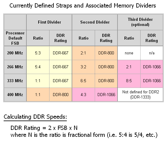
Because of this, the motherboard does not need to know anything about the installed processor and memory, other than the default FSB and the memory's SPD rating, which are both read programmatically prior to Power On Self Test (POST). For example, a 266 FSB processor paired with DDR2-800 memory will make use of the associated 266 strap's second divider - as would a 333 FSB processor. Would you be surprised to learn this works exactly the same way for a 200 FSB processor? Well, it does, and in fact it does not matter which processor type is installed - all combinations work and allow for the same exact memory speeds - DDR2-667 and DDR2-800 (and sometimes DDR2-1066).
If slower memory is detected the system simply uses the first divider in order to achieve DDR2-667 speeds. In the case of faster memory, the third divider is used for DDR2-1066 - which is sometimes available, depending on the strap in use. (All 266, 333, and the upcoming 400 MHz FSB parts will be able to make use of this new official memory speed, as recently announced by JEDEC.) One final note, "down" dividers are no longer possible with Intel platforms and as such the lowest supported memory speed for systems that will make use of the QX9770 (when it arrives) will be DDR2-800, unless the user chooses to underclock the FSB.
As we can see, this system allows for maximum component interchangeability and configuration flexibility all through the use of relatively straightforward selection logic. Check the table below for more information on how to derive these numbers.
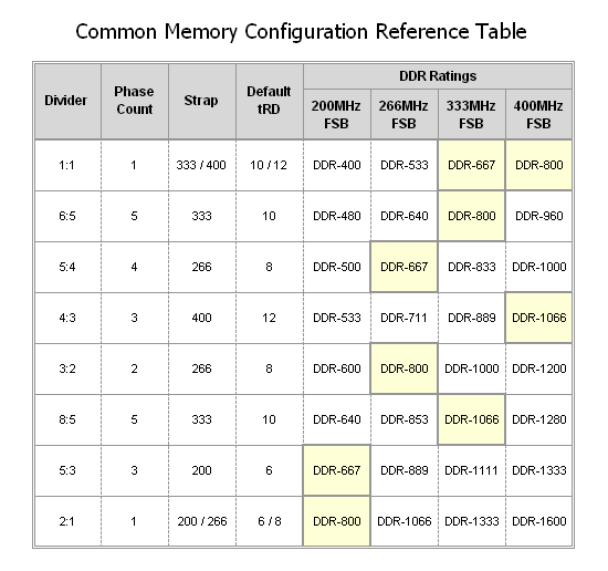
Now that we know a little more about what straps are and how they work, we are ready to discuss what they mean when overclocking. Let's say you have an E6700 that makes use of a default FSB of 266MHz - pushing the FSB to 400 while making use of the processor's default strap's second divider (3:2) results in a final memory speed of DDR2-1200, a goal that might be outside the realm of normal achievement unless you have memory capable of this speed. By selecting the 400 strap the 1:1 and 4:3 dividers become available and we are able to set a more modest speed of either DDR2-800 or even DDR2-1066. Alternatively, choosing the 266 strap permits use of the 5:4 divider for DDR2-1000.
The point is that the freedom to choose any strap we want, regardless of CPU type installed, gives us the choice to make use of a whole myriad of memory speed settings that would otherwise be unavailable. Take note of the "Default tRD" column; you will see that each strap has an associated value (6 at the 200 strap, 8 for 266, etc.) We will discuss this particular setting in detail a little later.
Until now, choosing a memory divider in order to set a final memory speed was easy. Most users focus solely on achieving maximum CPU frequency, letting the memory speed fall where it will. Although it is possible for memory to be the limiting component when overclocking, this is unlikely considering the low cost and high availability of today's performance DDR2 modules. Thus it's easy to pick a memory divider that places the memory operating point near a maximum without ever considering what could be done in order to further improve performance.
Perhaps too many users feel the time they need to invest in fine-tuning their memory settings is not worth the effort. While this might not be far from the truth, we find this hard to believe. Major memory manufactures like OCZ, Corsair, Cell Shock, G.Skill, and Team Group have entire departments of support personnel that work hard every day to provide users the assistance they need to make the most of their purchase. These groups are inundated with requests for help, from both experienced users and novices alike.
Going back to what we said before, what does all of this have to do with better performance on a clock-for-clock basis? In a word: everything! We would like to provide some solid information on the subject as to why the age-old quest for maximum FSB is not always the best approach; in fact, it is often the wrong approach. Our hope is that once allowed an opportunity to make use of this information, users will begin to understand the true limitations of their system components better and might perhaps stop inappropriately blaming overclocking failures on perfectly good hardware. Better yet, they'll stop buying boards based solely on FSB capability when overall system performance is much more important.
Now that we have had a chance to review the basics on memory straps let's move on to something a little more interesting - MCH clock crossing operation and the associated MCH Read Delay (tRD).
The Clock Crossing Procedure and MCH Read Delay (tRD)
Have you ever stopped to wonder how the Memory Control Hub (MCH) manages to transfer data from the system bus (FSB) to the memory bus and vice versa? Maybe you questioned why it was not possible to run your memory at any speed you desired, independent of the selected FSB. While there have been some chipsets that provide this capability, performance was rather spotty at times depending on the particular settings in use. In fact, these systems often resulted in the creation of rather large ranges of bus speed and memory speed ratios that refused to function, stable or otherwise. The concept was certainly fair enough, but at the time a well-engineered implementation turned out to be far more difficult that anyone may have been willing to concede. It should not come as a surprise that Intel chipsets have only allow the use of certain validated memory ratios - those same numbers we have grown to love (or hate) like 1:1, 5:4, 3:2, and so forth.
Back in the days of relatively slow-paced memory performance improvements, Intel had no problems pumping out processors with default FSB values that made running memory at synchronous speeds an expensive proposition. Thus they created the "down" divider that allowed the memory subsystem to run at a bus speed below that of the system bus. This allowed for a period of innovation where processor bus architecture was able to improve without placing an undue burden on the memory industry to create reasonably priced modules capable of these increased speeds.
In a lot of ways this also prevented cost-prohibitive aspects of validating higher data transfer rates from ultimately affecting the market as a whole. Because Intel was not obligated to allocate additional funding for the completion of this expensive process, the savings (however small) could be passed on to the consumer. When coupled with the added benefit of allowing for the purchase and use of lower-binned memory, we can easily see why a move such as this helped stimulate the industry into a period of unprecedented growth.
Today's market is much different. Older signaling technologies like Advanced Gunning Transceiver Logic (AGTL+), used almost exclusively by Intel in their monolithic CPU-to-MCH interface architecture, have just about reached the practical limits. As such, "up" dividers, those that allow for memory bus speeds in excess of the system bus speed, are used almost exclusively by high-performance systems. Indeed, it would be hard to imagine ever being satisfied with a system able to make use of memory operating at transfer rates of up to DDR2-667, and no higher. As odd as it may seem, the next generation of memory (DDR3) is based entirely on the concept of running at speeds mandating the use of at least a 2:1 memory bus to system bus frequency ratio.
When examined from this aspect it becomes clear what DDR3 really is - an early look at the next generation's mainstream memory component. Only when Intel has removed the performance barrier of their antiquated FSB and loosely-coupled MCH will we be fully able to finally experience the real improvements that DDR3 promises to provide. But we digress - speculating about what could have been done better or things to come is trite. Instead, let's concentrate on what can be done now to improve the collective performance of our systems.
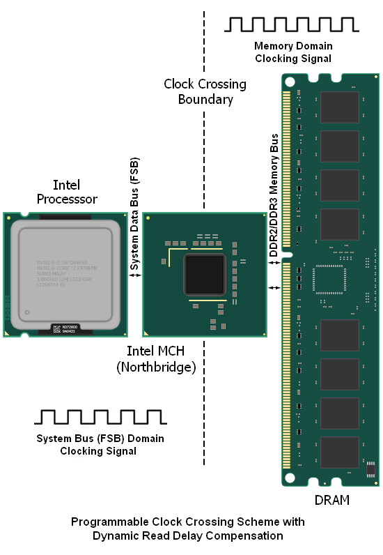
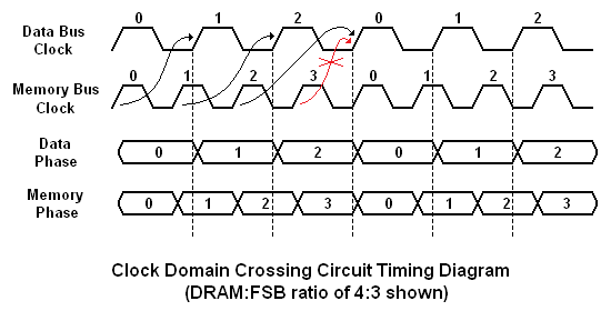
Below is a somewhat basic representation of the problem at hand (and later we will introduce the fairly elegant solution that Intel has crafted in order to tackle said problem). Are you still wondering what the problem is? Put briefly: designing an effective means for transferring data from one bus "domain" to the other, while still respecting the timing requirements for each bus.
We made mention earlier that we believe Intel's solution to be quite elegant. While this is true, the system is still far from perfect as it introduces a significant amount of extra data access latency to each and every memory read request. It might seem ironic that the design initially constructed in order to allow for higher memory speeds ends up being the very reason for the additional latency penalty incurred, but this is the case. Coincidentally, we can apply a similar accounting of the system's flaws when explaining why actualized system performance improvements are always far less than predicted when making use of the larger dividers.
Moving data between two simultaneously running parallel buses requires a fine level of timing control and a fair amount of programmable logic to be successful, especially if the scheme is to remain flexible. The graphic below should help to illustrate the concept. Four memory data clock cycles for every three system data bus cycles (a 4:3 DRAM:FSB memory ratio) means that the MCH can do little more than queue up data requested from the memory for transport to the system bus.
This process works to ensure that no FSB cycles are left unused, but it does little to improve actual memory throughput. Because of this, the gains seen are largely due to the increased transfer efficiency. For the same reason, sustained data rates, while improved, are made at the expense of requiring added latency associated with the transfer scheme. This has the affect of retarding the responsiveness of short bursts of random read activity. Some users [Ed: Androids in disguise?] even swear that they can tell when they are using an Intel system because of the suppression of the "snappy" experience that comes when using true low-latency systems.
In order to better quantify exactly how the MCH clock crossing procedure influences system performance, it might be helpful to take a step back and examine the different component parameters that contribute to a system's overall memory read (access) latency. The diagram below helps to illustrate just this point - we have identified each distinct operation that takes place during a CPU data request and the sum of the individual latencies that involved with each part of the process make up the total system memory access latency, as measured. As we will see, this time - expressed in nanoseconds (ns) - is critical to overall system performance.
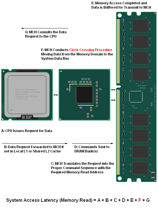
Although the user has at least minor control over just about every aspect of the system as modeled above, there are a few settings that when altered have the potential to drastically impact performance for the better (or worse, depending on how well you understand what you are doing). One of the most well known is the selection of primary memory timings (tCL-tRCD-tRP-tRAS). You may be surprised to learn that the effect of properly setting these values, represented by part "E", is quite insignificant when compared to your choice of tRD (the singular consideration in developing the latency associated with part "F"). This will be our focus for the remainder of our discussion. We have already lightly touched on this mysterious setting on the prior page.
MCH Read Delay Scaling and Default tRD Settings for Each Strap
Earlier, when we introduced the concept of the memory strap, we also included a table of common memory configurations that contained a column of "Default tRD" values. It's important to realize that these values are associated with the strap and have nothing to do with the actual FSB setting. This is because default operation assumes no overclocking, therefore if the 266 strap is being used then the processor obviously must be running at its rated FSB speed of 266MHz. Adding to this the element of a fully adjustable FSB introduces a new level of complexity that the system was never designed to handle.
This allows us to explain why making use of lower strap settings at one time provided for higher levels of performance - we've created the table below for just this purpose. (We say "at one time" because, as we will soon learn, most motherboards now implement strap changes in a manner much different than was previously done.) For example, selecting the 400 strap and setting a 1:1 memory divider at 400MHz FSB would result in DDR2-800 memory speed. By converting the FSB frequency into a cycle period (time for each clock tick) and then multiplying this value by the strap's default MCH Read Delay (tRD) we can effortlessly calculate the true latency (in nanoseconds) associated with this setting. As an example, dividing 1000 by the FSB (400MHz) gives us 2.5 (nanoseconds) - the co-efficient of 1000 used in this conversion formula was purposefully selected in order to give our result in the proper units. So, 12 times 2.5ns equals 30ns, which we then pair with our derived DDR speed rating of DDR2-800.
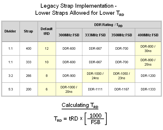
We will go into more detail about what this value means, but for the time being simply recognize that we want to minimize this number. We can see that the optimal configuration is one in which we would make use of a lower strap along with a higher FSB. While simultaneously applying these two considerations is obviously paramount in order to take advantage of this affect, the practical application of this approach is bounded in a number of ways. For instance, the near absolute minimum limit on any true read delay latency (tRD) might eventually come into play. We also need to be mindful of which memory dividers are available for the strap of choice, as these will ultimately dictate what final memory speeds are possible. Finally, we will soon learn that there are some strict rules that define whether or not a particular MCH Read Delay (tRD) is allowable, depending on the FSB, memory divider in use, and even the memory Column Address Strobe (CAS) setting.
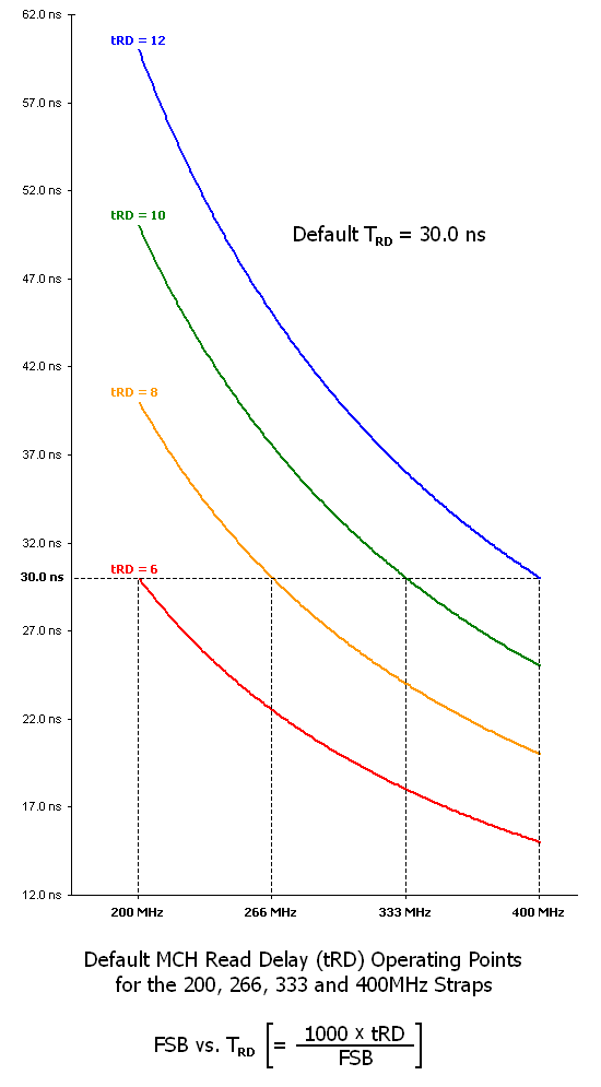
Now that we have had a chance to apply the simple equation to convert a tRD value into a TRD latency, we are ready to examine a graphic that displays the full breadth of this concept. We have plotted the complete range of FSB speeds encompassed by currently defined straps versus the derived TRD values for each default tRD associated with each strap. That may sound more complicated that what it really is; basically, these lines represent how TRD scales across our FSB window of interest (266 to 400MHz FSB) for each tRD in the table above. We can see that by drawing a vertical line from each default FSB up to the line corresponding to that strap's default tRD, and then reading across always results in the same TRD - 30.0 ns. This is by design, and is precisely how each default tRD was determined for all of the straps we have examined. It may be helpful to think of tRD as another memory timing, except that it has nothing to do with memory and everything to do with the MCH. In this sense it responds to FSB scaling in the same way as other memory timings - CAS (tCL), RAS to CAS (tRCD), Row Precharge (tRP) - the true latency (TRD) always decreases in a manner inversely proportional to FSB, and at some point will reach a minimum where the next higher tRD must be used in order to continue scaling.
What happens if we can set the tRD independent of the strap in use? Of course, the strap selected would still dictate which memory dividers are available, but no longer are we forced to make this change solely for the purposes of modifying tRD. As it turns out, this is exactly how these settings work with most of today's enthusiast motherboards built for overclocking, and the ASUS Rampage Formula is no exception. The ability to set a tRD value, regardless of the strap (i.e. memory divider), allows for a whole new world of possibilities when tuning for enhanced performance.
This brings us to the focus of true improvements made to the X38 chipset, which can be experienced more easily with X48 now. Too many benchmark reviews have been guilty of inappropriately discounting the value of this new chipset by calling the X48 little more than a "speed binned" version of the X38 and then comparing their relative performance at stock speeds. This would be like calling the QX6850 (3.00GHz default clock) a speed binned version of the Q6600 (2.4GHz default clock), benching them head-to-head at an equivalent speed, and then concluding that the QX6850 provides no additional value. Overclocking headroom is exactly what differentiates Intel's current line of Core 2 Extreme CPUs from their mainstream offerings, and it's also what makes the X48 stand head and shoulders above the X38 now that the BIOS designs have matured. When all is said and done, this just makes us wonder who really understands how to overclock the MCH properly.
MCH overclocking takes many forms. One form is something you might already be familiar with, carried out by simply raising the FSB. The problem is that BIOS setup routines will usually provide relief to the MCH by automatically relaxing tRD as the FSB is pushed higher and higher. This effect can easily negate any gains that might otherwise be achieved. Taking control of tRD and manually steering it to a lower value will allow the user to retain the associated performance increase, and as such must also technically be considered overclocking. As with most if not all positive performance adjustments realized while overclocking, this modification comes at a cost - in particular, the need for increased vMCH.
That is not to say that a certain level of headroom does not already exist as an accessible performance boost - it does. While Intel is wise to provide generous levels of margin between pre-established default tRD values and those attainable without the need for any additional voltage, we would consider ourselves foolish if we did not take advantage of this relatively free performance improvement. For instance, looking at the plot of X48 MCH overclocking response curves below we can see that although a default tRD value of 12 is normally used at greater than 400MHz FSB (using the 400 strap), at about 425MHz FSB we should have little to no trouble setting a tRD of 6, even using stock vMCH. The end result this tRD reduction of 6 clocks brings is a total memory read latency decrease of approximately 14.1ns (the difference in TRD values at 425MHz FSB using a tRD of 12 and 6).
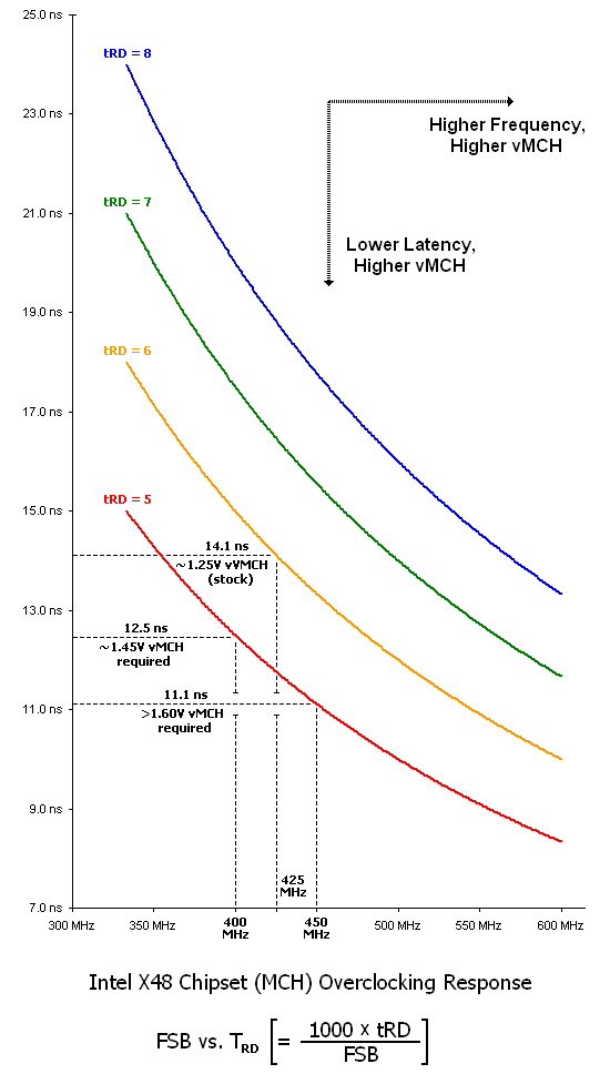
With that, we can finally see how this consideration comes full circle - the lower the TRD, the higher the memory read performance and vice versa. This change in TRD also drives vMCH, with lower values requiring substantially more voltage than the more "relaxed" (higher) values. We were able to push our ASUS Rampage Formula to a very impressive 450MHz FSB using a tRD of 5, which correlates to a TRD of about 11.1 ns. Because this required about 1.60V vMCH, for all intents and purposes we would consider this to be the practical limit of scaling, at least with conventional cooling. Above this voltage, we find that the X48 quickly turns into a little furnace during periods of prolonged load. Our recommendation is the liberal use of extra cooling capacity if you feel the need to push any further.
Real-World Results: What Does a Lower tRD Really Provide?
Up until this point we have spent a lot of time writing about the "performance improvement" available by changing just tRD. First, let's define the gain: lower tRD settings result in lower associated TRD values (at equivalent FSB clocks), which allow for a lower memory read latency time, ultimately providing a higher memory read speed (MB/s). Exactly how a system tends to respond to this increase in available bandwidth remains to be seen, as this is largely dependent on just how sensitive the application/game/benchmark is to variations in memory subsystem performance. It stands to reason that more bandwidth and lower latencies cannot possibly be a bad thing, and we have yet to encounter a situation in which any improvement (i.e. decrease) in tRD has ever resulted in lower observed performance.
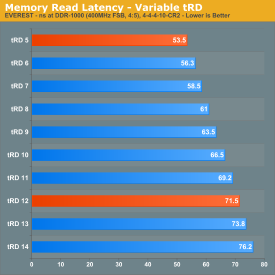
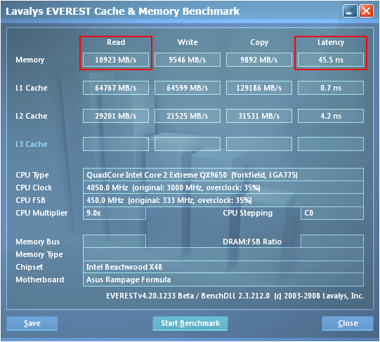
EVEREST - a popular diagnostics, basic benchmarking, and system reporting program - gives us a means for quantifying the change in memory read rates experienced when directly altering tRD though the use of its "Cache & Memory Benchmark" tool. We have collected these results and present them below for your examination. The essential point to remember when reviewing these figures is that all of this data was collected using memory speeds and settings well within the realm of normal achievement - an FSB of 400MHz using a 5:4 divider for DDR2-1000 with 4-4-4-10 primary timings at a Command Rate of 2N. The only change made between data collection runs was a modification to tRD.
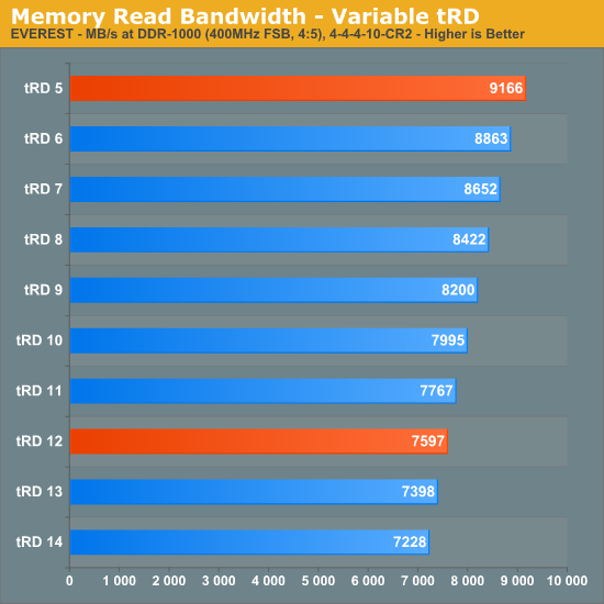
Using the default tRD of 12, our system was able to reach a maximum memory read bandwidth value of 7,597 MB/s - a predictable result considering the rather relaxed configuration. Tightening tRD all the way to a setting of 5 provides us with dramatically different results: 9,166 MB/s, more than 20% higher total throughput! Keep in mind that this was done completely independent of any memory setting adjustment. There is a central tenet of this outcome: because the MCH is solely responsible for delivering the additional performance gains, this concept can be applied to any system, regardless of memory type or quality.
The next graph shows how memory access (read) latency changes with each tRD setting. As we can see, the values march steadily down as we continue to lower tRD. We can also note that the change in latency between any two successive steps is always about 2.5ns, the Tcycle value for 400MHz FSB and the expected equivalent change in TRD for a drop in tRD of one. No other single memory-related performance setting has the potential to influence a reduction in read latency of this magnitude, not even the primary memory timings, making tRD unique in this respect. For this reason, tRD is truly the key to unlocking hidden memory performance, much more so than the primary memory timings traditionally associated with latencies.
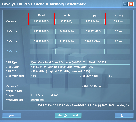
We realized our best performance by pushing the MCH well beyond its specified range of operation. Not only were we able overclock the controller to 450MHz FSB but we also managed to maintain a tRD of 5 (for a TRD of about 11.1ns) at this exceptional bus speed. Using the 3:2 divider and loosening the primary memory timings to 5-5-5-12 allowed us to capture some of the best DDR2 memory bandwidth benchmarks attainable on an Intel platform. As expected, our choice of tRD plays a crucial role in enabling these exceptional results. Screenshots from EVEREST show just how big a difference tRD can make - we have included shots using tRD values of 7, 6, and 5.

A considerable share of the memory read performance advantage that AMD-based systems have over Intel-based systems can be directly attributed to the lower memory latency times made possible by the design of the AMD processor's on-die memory controller. So far we have done a lot to show you why reducing TRD to a lower level can make such a positive impact on performance; knowing this you might tend to believe that the optimal value would be about zero, and you would be right. Eliminating the latency associated with the MCH Read Delay would further reduce total system memory read latency by another 12.5ns (as modeled by the results above).
Given this, Intel-based systems would perform memory read operations about on par with the last generation AMD-based systems. Although not the only reason, this is one of the main motivations behind Intel's decision to finally migrate to a direct point-to-point bus interface not unlike that which has been historically attributed to AMD. Removing the middleman in each memory access operation will do wonders for performance when Intel's next step in 45nm process technology, codenamed Nehalem, hits the shelves in ~Q4'08. Until then we'll have to try to do the best with what we've got.
The Rules of Working with tRD: What's Allowed and What Isn't
We mentioned earlier that there are a few rules pertaining to the modification of the default tRD value for a particular memory subsystem configuration. These rules are actually more of a set of equations that we have derived in order to assist the user in pre-determining whether or not a system will POST and operate given the settings in question. They can also be used to explain after the fact why certain configurations refuse to function.
In actuality, there is only one requirement that must be satisfied when setting tRD: The MCH must have a minimum amount of time to complete the clock crossing procedure for each data bit translated from one clocking domain to the other. We have shown the equation below for those that care to know. Unfortunately it does not lend itself well to being solved as the input variables ("t0" and "tckxss") are not readily obtainable.
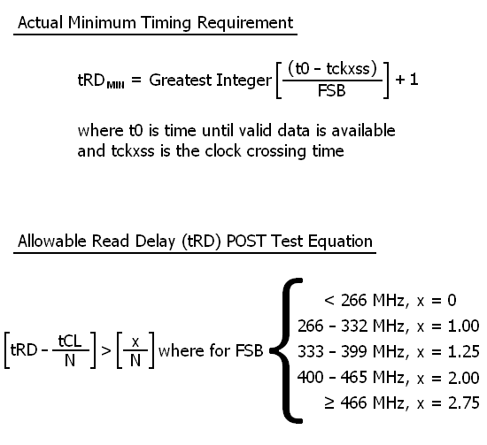
"t0" is the total time it takes data being returned to the CPU as read in memory to cross from the memory bus domain to the system data bus domain. This is dependent on a number of variables, including memory burst length (4 or 8 cycles), Command Rate (1N or 2N), the memory divider in use, CAS (tCL) timing, and the current FSB. "tckxss" is a little more esoteric in nature and is outside the scope of this discussion; the value is generally very small when compared to "t0". The difference in these times, rounded to the lowest integer plus one, bounds the lowest potential tRD setting necessary for data to be properly transferred from one bus to the other.
Because the first expression is too difficult to warrant everyday use, we spent many hours populating a large test matrix table created for recording the POST (Power On Self Test) results of every strap/divider/FSB/CAS setting combination that our test bench was physically capable of supporting. Using this data, we then developed the method and equation you see above, which can determine whether or not a desired memory subsystem configuration will work. It is possible, and rather probable, that there is another step discontinuity in the logic for FSB speeds in excess of the high value in our test range (466MHz). We will leave the discovery of some such value up to others - unless Intel is kind enough to send us additional 45nm dual-core processors, in which case further testing on our part might be justified.
Entering arguments for the use of the "POST Test Equation" are as follows: tRD, in clocks; tCL (CAS), in clocks; FSB, in megahertz (MHz); N, the memory divider in use, expressed in fractional form (i.e. 3:2 would be 3/2); and "x", which should be chosen from the options provided, depending on the FSB in use. Evaluate the left and right side of the equation separately. The expression is satisfied if the left (actual margin) is greater than but not equal to the right (the minimum required margin).
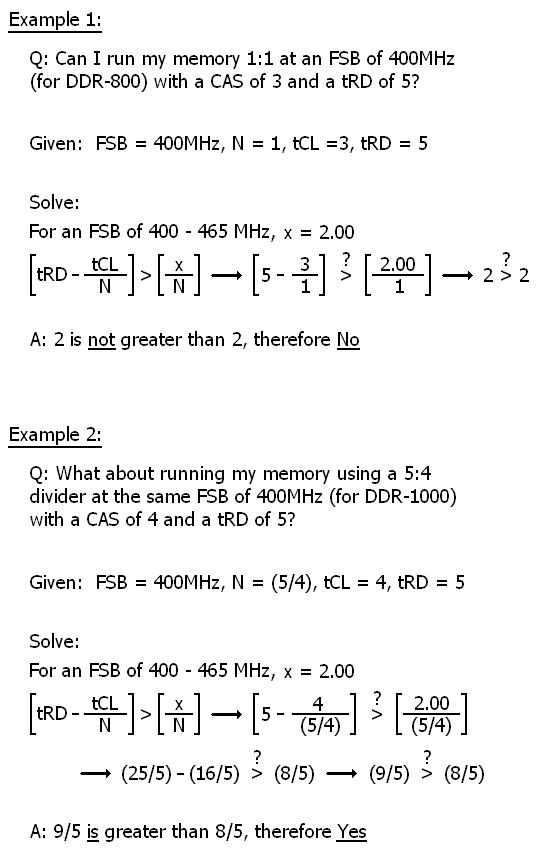
There are no units purposefully associated with these numbers, as this equation is intended as nothing more than a test to determine whether a system will POST using the desired parameters. If the expression is false, the configuration/system will fail to boot; if it is true then the configuration is allowed and the POST event should at least occur. Keep in mind that this equation provides absolutely no assurance that the system will be stable at the settings provided - just because you want to run your memory at DDR2-1200 CAS 3 and the equation says this is possible, does not mean that your wish will be fulfilled. Let's go through a quick exercise of what we have learned regarding the proper use of the "POST Test Equation" with a few practical examples.
If you can follow these examples then you are ready to move on to the next step - determining optimal system performance points and then validating your results. There are many choices when it comes to deciding how to configure a system for the best possible experience. Some choices are clearly better while other decisions may come to down to personal preference. For instance, some users may be willing to subject their expensive hardware components to higher voltages, creating an environment of accelerated wear and earlier failure. Others may be far less concerned with the consequences of their choices; in either case the trade-offs will be clear. We will now take what we have learned and provide our rationale for why we would feel one overclocking approach to be superior to another. After all, overclocking should always be based on an intelligent decision making process and not the clumsy application of brute-force.
How to Choose an Appropriate Memory Configuration
Now that we have seen what impact tRD can have on memory performance, and we know how to determine whether certain memory configurations will work or not, the easiest way to go about deciding how to set up memory is to concentrate this knowledge into a table of candidates and then choose the best one. As you can see below, we have done just that.
Four target FSB frequencies (400, 450, 500 and 550MHz) were used in the construction of these tables. We chose these values because they represent the approximate best-case bus speeds for each tRD setting of concern (5, 6, 7, and 8). As we wrote earlier, the MCH can be overclocked in both the traditional sense - by raising the FSB - or by simply lowering the tRD from the default value at a specific bus speed. When these two effects are combined, the resulting strain on the MCH often requires a considerable amount of extra voltage in order to maintain stability. Because of this, MCH base operating frequency (i.e. FSB) increases detract from the ability to achieve the same low TRD values available at lower bus speeds. One of these two approaches to overclocking the MCH must be better than the other - the only question is which one is best? As it turns out the answer involves a delicate balance for each approach. Before we review our final recommendations, let's look at the contenders.
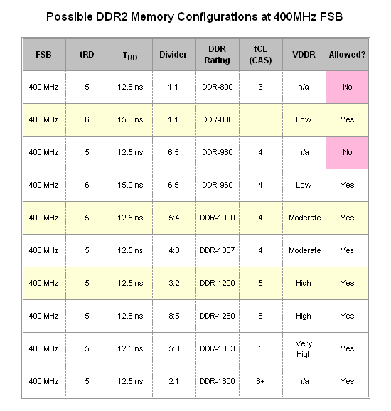
For the 400MHz FSB case three configurations stand out in particular - 1:1 for DDR2-800, CAS 3; 5:4 for DDR2-1000, CAS 4; and 3:2 for DDR2-1200, CAS 5. Of these three the last two are actually more appealing, not only because they offer the potential for higher memory bandwidths but also because a tRD of 5 is allowed for these configurations whereas CAS 3 operations using a 1:1 divider at 400MHz FSB is not possible with a tRD of 5. These results can be predicted using the "POST Test Equation" provided on the previous page. Those that choose to operate at 400MHz FSB (assuming this bus speed can be appropriately matched with one of their processor's available multipliers) need to decide whether to run the 5:4 or 3:2 divider. The decision might come down to the amount of memory being used - DDR2-1200 can be a rather lofty goal with four DIMMs installed, in which case DDR2-1000 would be the next best choice.
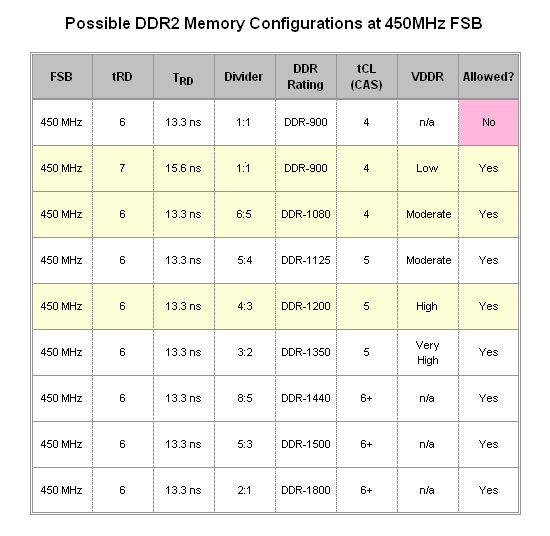
Moving on to the analysis at 450Mhz FSB, although we are able to show impressive memory read speeds at this same bus frequency using a 3:2 divider for DDR2-1350 CAS 5 at a tRD of 5, this configuration was far from stable on stock cooling alone - as was the memory speed. Most likely, the need to loosen tRD to 6 will be inevitable at this bus speed. Right from the start, we can see that TRD takes a hit as our minimum values thus far came at the lower 400Mhz FSB. What's more, possible memory configurations at this FSB do not seem to offer any real improvement over those at 400MHz. The first option worth considering, DDR2-900 at CAS 4, can be a little slow, especially considering that a tRD of 6 is not allowed. The DDR2-1200 choice will provide (at best) only miniscule gains over the same memory speed at 400MHz FSB because of the additional throughput efficiency made possible by the higher bus speed. Then again, the increase in TRD to 13.3ns, up from the minimum value of 12.5ns at 400MHz FSB, may completely negate any chance of a performance gain. Our last contender, DDR2-1080 at CAS 4, might be another neutral choice - on one hand there could be a small gain in performance over DDR2-1000 (CAS 4) seen at 400MHz FSB, but again the higher TRD may be this configuration's undoing.
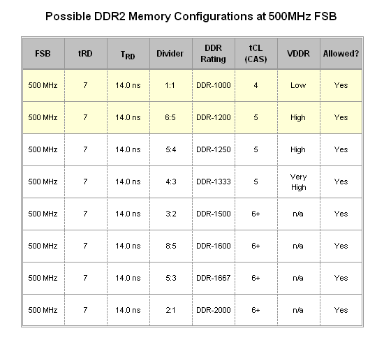
The meaningful choices at 500MHz FSB are even bleaker - here we find only two that merit any kind of attention (although you might be able to argue a point for the DDR2-1250 configuration). Having to further loosen tRD to 7 only compounds the issue of the slipping TRD value that we first saw at 450MHz FSB. On top of this, the DDR2-1000 CAS 4 and DDR2-1200 CAS 5 memory speeds are not unique to this FSB, effectively removing any incentive in choosing this bus frequency. Furthermore, the 4:3 and greater dividers are practically worthless as they attempt to push DDR2 memory to mostly unattainable speeds. Considering this, there is only one reason we would ever recommend bus speeds this high and that would be in the case of a severely limited CPU multiplier in which the extra FSB is required by the processor alone.
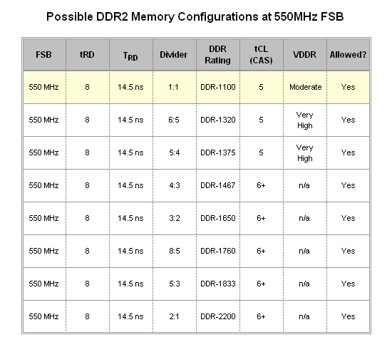
Without a doubt, 550MHz FSB represents the coup de grâce of ridiculously high bus speeds with only one divider (1:1) providing any substance to this horrible choice in settings. Again, we see the uncontrollable relaxation of TRD (at 14.5ns), which when coupled with a memory configuration of DDR2-1100 at CAS 5 certainly does not create a situation worth writing home about. Why anyone would choose to run their system this way is beyond us.
If there is one thing our studies here should teach us, it's the futility of searching for maximum performance in outrageously high bus speeds. Truthfully, we would argue that the best selections are possible at the "low" FSB of 400Mhz. Let us make it perfectly clear by saying that none of us here at AnandTech would ever tell you that 400Mhz FSB is an inferior choice. In fact, many of us make heavy use of this exact bus speed when setting up our personal systems for daily use. In the interest of fairness, let's take one last look at all of the highlighted configurations from the tables above.
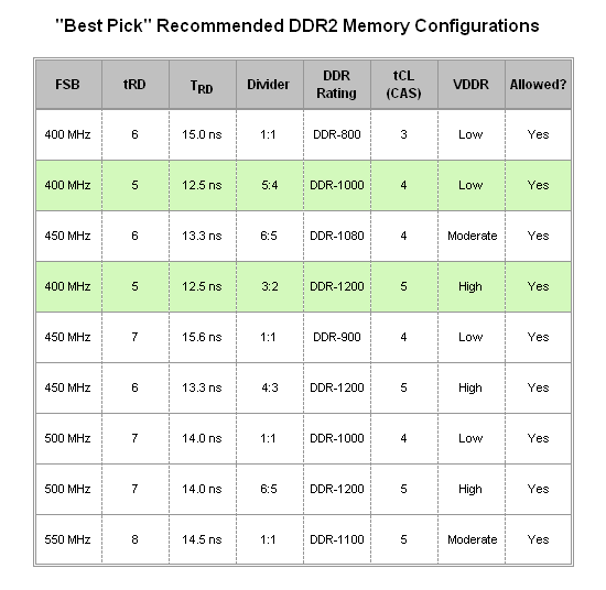
When viewed together the task of picking out a couple of the best choices becomes rather simple. A+ ratings, of course, go to the two configurations colored in light green (5:4 for DDR2-1000 CAS4 and 3:2 for DDR2-1200 CAS 5). You may be surprised, as we mentioned earlier, that they both use a humble 400MHz bus speed. If forced to choose another option, close second place awards might go to 450Mhz FSB - 1:1 and DDR2-900 CAS 4, or 4:3 DDR2-1200 CAS 5 (assuming your motherboard is capable of stable operation with the sometimes poorly implemented 4:3 divider). Just do not forget - whatever memory option you choose, be sure to remember the importance of tRD.
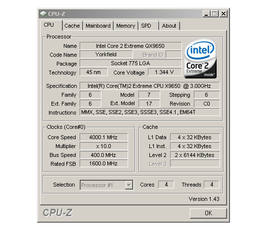
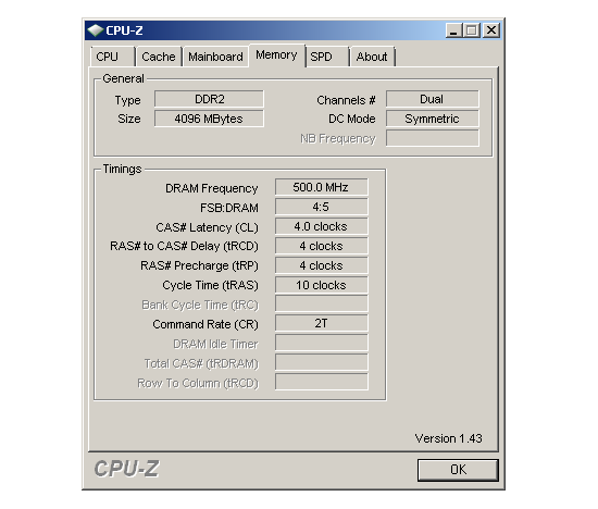
In the end we decided to run our Intel Core 2 Extreme QX9650 at a final FSB of 400MHz with a multiplier of 10.0x at an even 4GHz. Our 4x1GB of OCZ DDR2 PC2-8000 Platinum Extreme Edition memory was set to run at DDR2-1000 (5:4) CAS 4 with a tRD of 5. Ultimately, the ASUS Rampage Formula provided us the ability to build a well-tuned system. Without question, ASUS' addition of BIOS options for direct tRD manipulation was instrumental to our successful overclock. When paired with top-end GPUs from either ATI or NVIDIA, our rig becomes a formidable gaming platform for enjoying today's titles and beyond.
Conclusions and Final Thoughts
Our experience with the ASUS Rampage Formula has been tremendously enlightening thus far. Although we can confidently claim a long-standing familiarity with MCH Read Delay (tRD) and its affect on overall system performance, this motherboard provided us exactly the foundation we needed to develop our current understanding of just how some of these previously elusive settings really work. There is no reason why any enthusiast should not be able to arm themselves with this information in their quest for the perfect overclock based on overall system performance. We sincerely hope that the Rampage Formula is the first of many boards from ASUS to incorporate this kind of great innovation. We have grown accustomed to using it now, and we don't want to go back to the old methods of manipulating tRD.
The Rampage Formula's layout is as close to perfect to possible - water-cooling enthusiasts will have no problems fitting two ATI graphics cards in Crossfire, even when installing full-coverage water blocks. Through-hole mounting for the Northbridge and the ability to remove the stock cooling solution without disturbing the portion covering the MOSFETs in the power delivery circuit is especially nice. Fitting an after-market heatsink on the MCH will be simple and straightforward. Then again, this may not be necessary; we actually found the X48 to be cooler than the X38 in the production level boards.
The ability to use DDR2 is another great benefit to consider when selecting an X48 board. Again, ASUS has made the right choice in this arena and has decided to provide separate solutions based on each memory type. For the ultimate in performance, though, we suggest you check out DDR3 based configurations if you can afford it.
We anxiously await the impending availability of this board; we know that its release - and that of its DDR3-based "Extreme" brethren - has the potential to usher in a new round of 3D performance records from today's top overclockers. The early maturity of ASUS' BIOS coupled with the capabilities of the Intel X48 chipset make a fantastic combination for achieving absolute top speeds. For those of us more firmly grounded in reality, rest assured that we have a hard time finding reason not to recommend the use of this board in even the most demanding new systems.
It would be ignorant of us not to expect other companies such as MSI, abit, DFI, and Foxconn to follow suit with the introduction of their top-end X48 boards. In fact, just last week we took an in-depth look at the Gigabyte GA-X48T-DQ6 and what it had to offer. Although it's not quite as strong out of the gate, given time we expect BIOS improvements to close the gap. The Gigabyte board also uses newer DDR3 technology, so whether or not ASUS' comparable board will experience the same types of problems remains to be seen.
One thing is for certain, Intel and ASUS have teamed up to bring us another great overclocking choice that sets a new standard in the market. Early reports of limited performance improvements may have tempted you sit out the X48 release. Based on our results from the ASUS Rampage Formula, we will go on record now and reject our previous position. We will be running X48 boards in our personal systems; what about you?


