Original Link: https://www.anandtech.com/show/2410
The Gigabyte GA-X48T-DQ6 - Redefining the High End?
by Rajinder Gill on January 2, 2008 3:15 AM EST- Posted in
- Motherboards
Gigabyte's motherboards are always products we look forward to, especially the budget/midrange solutions. These boards represent features and performance that often belies their price. Recently, Gigabyte has also been making strides into the high-end of the motherboard market. The first product of Gigabyte's aspirations using an Intel chipset was the GA-X38-DQ6 motherboard. The board was generally well received and had a decent set of features and performance. In short, we would not hesitate to recommend the GA-X38-DQ6 for a top-end overclocking or gaming system.
The only gripe about the GA-X38-DQ6 by hardcore overclockers is that it has slightly lower clock for clock performance when compared to other X38 motherboards. The GA-X48T-DQ6 we are reviewing here today obviously uses Intel's higher speed binned X48 chipset. Instead of just plugging the X48 into the existing X38 board design, Gigabyte listened to the concerns of users. Gigabyte made a wise decision to refine the existing X38 motherboard design to take advantage of the additional performance potential of the X48 speed bin.
A few months ago our feelings about the X38 chipset were a little mixed; we felt it really did not bring anything exciting to the table. As time has progressed since the chipset launch, motherboards based on the X38 chipset have become our favorites for overclocking, for many different reasons. In fact, the primary reason is that they have proven to be extremely reliable for overclocking use on a 24/7 basis. Once set up correctly, we find these boards to be able to run the same settings day-in day-out, so long as the demands are reasonable. Naturally for the budget minded users, we would still lean towards the P35 chipset as far as single graphics card use goes. However, as the focus shifts, the prices of X38 based boards should come in lower than the higher end P35 boards, making the decision of which one to choose all too easy.
It really is no surprise that Intel CPU's are at their very best when teamed with Intel chipsets. Understandably, the release schedule of all the tier-one suppliers includes motherboards in either DDR2 or DDR3 format using either the X38 or the updated (speed binned) X48. While we have always felt that the synthetic performance figures of the X38 in DDR2 form have been lower than expected, the 3D performance gains over more attractively priced P35 chipset is always apparent. In DDR3 format the X38/X48 is the performance choice, and outperforms the DDR2 boards overall in just about every benchmark… well, at least by a few percent. Of course, this slight increase in performance comes at an expensive cost, with DDR3 memory prices being double that of DDR2 - if not more - depending on what speed bin you order.
A couple of weeks ago, we were able to provide a small glimpse of the high-end extreme benchmarking that the DDR3 based GA-X48T-DQ6 is capable of in current form. We managed a clean sweep of current single card 8800 GTS 640MB 3DMark world records using this motherboard. The board's overclocking performance impressed us, but using a motherboard in a normal operating environment like most users is always an important part of our testing. Things were still quite rough around the edges at the time of the preview. In fact, we were unable to install Microsoft Vista due to our boot drive being unrecognized as a valid partition after Vista had completed formatting the drive. Issues like these are not new to us; most of the boards always need BIOS updates in their early stages. Our real concerns at the time revolved around non-working memory dividers and general unpredictability when overclocking.
Things have certainly progressed in some areas since our first look; we have received a few BIOS spins addressing improvements and compatibility in several areas. In truth, this has not been the most solid pre-release board we have received of late. We were actually beginning to feel a little spoiled, as most of the X38 based pre-release boards we received have been remarkably ready for good overclocking right from the get-go. In spite of this, we decided to keep the length of time between the first look and our review as short as possible. This is especially important in light of the fact that we are endeavoring to provide users with meaningful BIOS insights before Gigabyte releases the board. Naturally, this process takes time, but we think it's well worth the wait considering the options available in the BIOS. Indeed, we are intrigued to see what Gigabyte has managed in bringing performance and reliability together in one package using the X48 chipset.
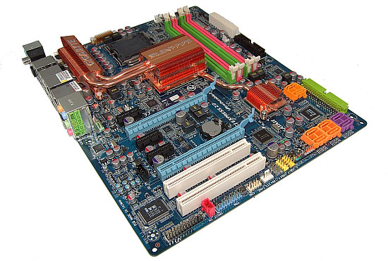
Board Layout and Features
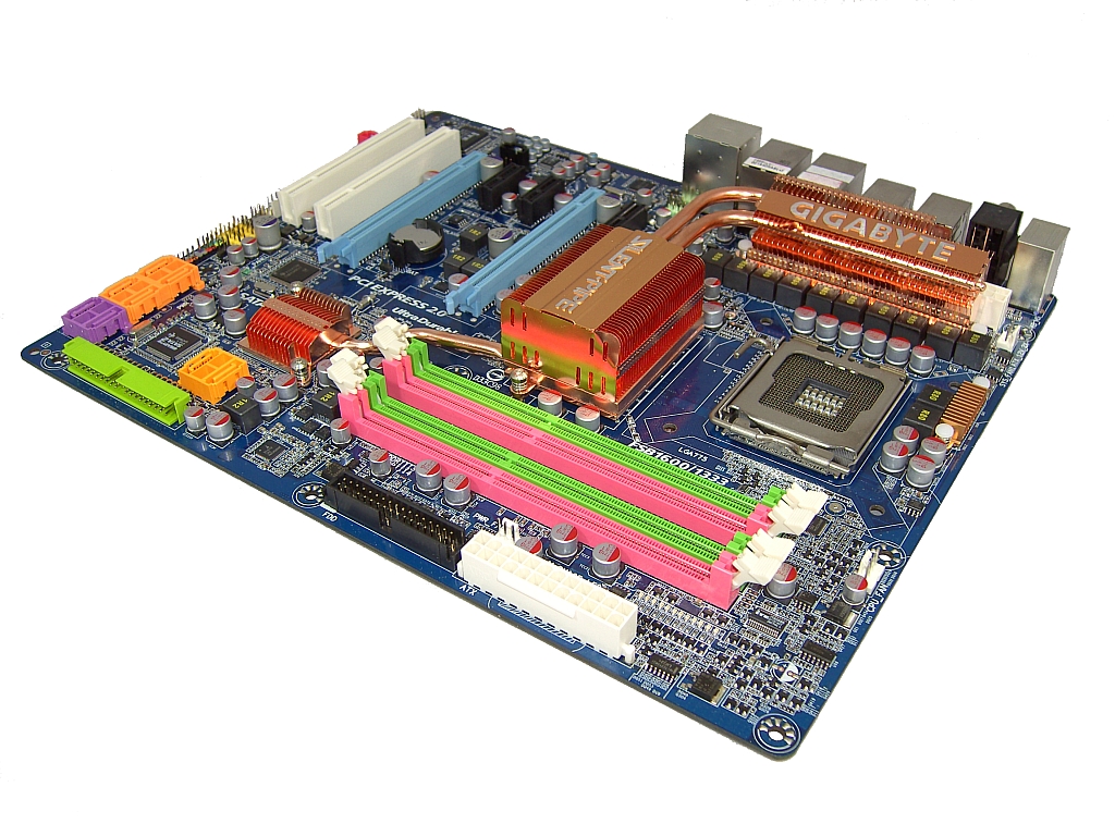 |
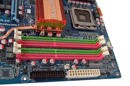
Though the color scheme of this board may seem a little garish (the pink and green memory slots are the worst offenders), it's the boards' features that interest us most. Gigabyte utilizes low RDS MOSFETs for the CPU PWM, memory, and chipset. The CPU power supply is a reported 12-phase design, utilizing five MOSFETs per phase. Gigabyte used the Intersil ISL6327 buck controller, which is only a 6-phase device, so in effect this is not a true 12-phase power supply as marketing materials would lead you to believe. Gigabyte's implementation of the ISL6327 controller is to feature a 3-step software controllable phase shutdown option, which is configurable via the supplied "Dynamic Energy Saver" OS software. We rather like the idea of user configurable phase control. When using quad-core processors for simple applications such as browsing the web, why not save motherboard power consumption by closing down some of the PWM phases? In truth, the power savings of this feature are not huge, but we still regard this as a step in the right direction from Gigabyte.
The memory and Northbridge power supplies are a dual phase design. The MOSFETs used by Gigabyte have a low conduction resistance and are of high quality. This allows for a wide power supply bandwidth and low output impedance, both favorable for overclocking. Dual phase memory power has been used by ASUS in their top-end boards for the last few months and has pretty much become "de rigeur" for companies who wish to compete with the excellent 4GB memory overclocking potential of ASUS motherboards. Not only has Gigabyte jumped on the dual phase power bandwagon for memory, they have also upped the ante by using dual phase power for the X48 MCH chipset. Clean power supply lines to the X48 chipset should easily help bring stock Northbridge voltage support of 1600 FSB to this motherboard.
We are advocates of dual phase memory power. High-speed DDR3 memory modules demand wide bandwidth and a low impedance power supply. A single MOSFET in this application may offer superior ripple rejection but will struggle to supply low impedance at high frequencies, especially if we consider the power draw of four overclocked DDR3 memory modules. Gigabyte has also tuned this board for DDR3-1900MHz memory speed, when using A-DATA's 2GB DDR3-1900 kit and XMP profiles. As usual, Gigabyte uses SMT solid polymer capacitors in all locations. There are eight fan headers to provide cooling options to all key motherboard areas. Fan control is offered via the supplied Easy Tune 5 Pro software for the CPU, System, and Power fan headers. Unfortunately, there are no onboard power and reset buttons. For users that want to benchmark this motherboard on an open test-bed, onboard switches would have been a welcome and expected addition at the price point. The onboard audio is supplied by the very good Realtek ALC889A codec that features DTS connect and full Blu-Ray and HD-DVD audio support.
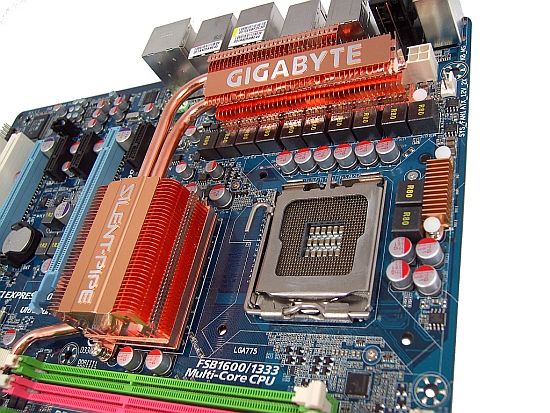
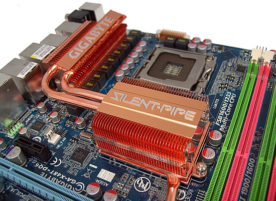
The CPU socket area is clean enough to allow the mounting of large CPU coolers. The issue is that Gigabyte has once again used their "Crazy Cool" heat plate behind the socket heatsink. This means that top-end air coolers that rely on a back-plate and screw mounting cannot be used on this motherboard without modifications to either the cooler or the motherboard. The Crazy Cool heatsink also doubles up as the retention bracket for the stock Northbridge cooler. Therefore, if the Crazy Cool heatsink is removed, the user will also have to find another means of securing the Northbridge heatsink to the board. In our opinion, Gigabyte could easily omit this heatsink design altogether, as it does virtually nothing to ensure better overall motherboard temperatures. Crazy Cool actually serves as a hindrance to those who wish to use top-end air coolers.
The 8-pin ATX power connector is located just behind the PWM heatsink at the top right corner of the picture. The Northbridge, Southbridge, and PWM heatsinks are connected via a heatpipe. Users who wish to water-cool any of these areas will need to replace the entire stock assembly with aftermarket cooling solutions. Lastly, stock Northbridge voltage is set to 1.45V on the latest BIOS we have received. This means that the chipset runs very hot, requiring active cooling with a good fan to ensure stability if this board is to be used for overclocking.
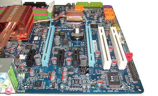
ATI CrossFire support is offered via two x16 PCI-E 2.0 slots. Three PCI-E x1 slots are available for use, though as always PCI-E x1 compatible devices are still not available in abundant quantities. Located at the lower end of the board are two PCI slots, with access to the lowest PCI slot even if CrossFire is used. The CMOS clear jumper is placed above the second PCI-E x16 slot, making it a little awkward to get to once a graphics card is inserted in either PEG slot. Gigabyte again uses their dual BIOS system, which features self-recovery in the event of a corrupt BIOS file.
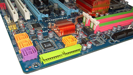
There are a total of eight SATA ports; six come via the Intel ICH9R Southbridge offering RAID 0, 1, 0+1, 5 or JBOD support. The other two SATA ports use Gigabyte's own SATA controller, offering RAID 0, 1 and JBOD support. The IDE connector sits to the right of the SATA ports, with enough clearance to make cable insertion easy, even when a long graphics card is used.
The IDE floppy and ATX 12V connectors are placed conveniently at the right edge of the motherboard; again, there is plenty of clearance around each connector to ensure ease of use.
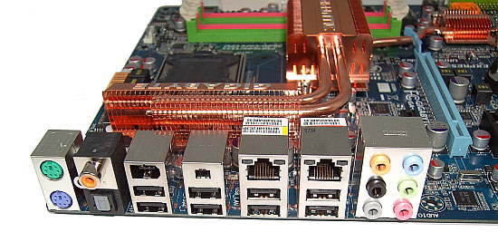
The rear I/O port features eight USB ports, S/PDIF and TOSLINK output, two IEEE 1394a ports, two RJ45 ports, and PS/2 keyboard and mouse ports. Six audio jacks are also available for the Realtek ALC889a onboard audio chip.
Gigabyte's supplied cable package consists of four SATA cables, an IDE cable, and an expansion bracket that provides two eSATA ports. The software bundle includes Easy Tune 5 PRO, which allows Windows based overclocking of the Front Side Bus as well as adjustment of CPU Vcore and memory voltages. There are a host of automatic overclocking features, which overclock the system when under load. Manual overclocking of graphics cards is also possible via the Easy Tune 5 interface.
Test Setup
| Gigabyte GA-X48T-
DQ6 Standard/Overclocking/Benchmark Testbed |
|
| Processor | Intel Core 2 Quad Extreme
QX6800 (Quad-core 2.93GHz 1066FSB 2x4MB Shared Cache) Intel Core 2 Quad Extreme QX9650 (Quad-core 3GHz 1333FSB 2x6MB Shared Cache) |
| CPU Voltage | 1.200V ~ 1.450V |
| Cooling | Water cooling: Swiftech Apogee GTX PA120.3 Rad 3 X Laing DDC Ultra Petra Top pumps in series 3x Panaflo 120mm Fans 7-10V |
| Power Supply | OCZ 1000W |
| Memory | OCZ DDR3 PC3-14400 (DDR-1800) Platinum
Edition 2x1GB XP, 4x1GB Vista 64-bit |
| Memory Settings | 5-5-5-12 1N (266 and 333FSB) 6-6-6-18 1N (400 FSB) 8-8-8-20 1N (450FSB) |
| Video Cards | MSI 8800 Ultra |
| Video Drivers | NVIDIA 169.09 (XP), 169.25 (Vista 64) |
| Hard Drive | Western Digital 7200RPM 250GB SATA 3/Gbps 16MB Buffer |
| Optical Drives | Plextor PX-B900A, Toshiba SD-H802A |
| Case | Lian Li -75 |
| BIOS | F3D |
| Operating System | Windows XP 32-bit SP2 |
| . | |
We decided to use our base QX6800 CPU with our standard tests run on the 9x multiplier to simulate the attractively priced Q6600 CPU and to compare against some of our previous benchmarking results. The QX9650 was used to cross-compare performance at relevant overclocks using our compact benchmark test suite. In this section of testing, we aim to remain within realistic cooling capacity temperatures and current CPU stepping capabilities. This better shows an overall picture of motherboard performance potential using widely available parts.
With such a vast array of overclocking BIOS functions at our disposal, we decided to stick with a single operating system environment for the overclocking tests. We selected Microsoft Windows XP SP2 due to its maturity, taking away some of the time burden looking for possible software level conflicts that may exist on a newer OS (though we ventured to run a compact Vista test suite for the non-overclocking benchmarks). The Vista tests were all run at board defaults, using an FSB multiplier combination of 9x333 and 4GB of memory with both processors.
We ran 1280x1024 resolution game benchmark tests in order to cross-compare CPU MHz related gains in our board specific tests. We utilize new drive images on each board in order to minimize any potential driver conflicts. Our 3DMark results utilize the standard benchmark resolution for each program. We run each benchmark five times, throw out the two low and high scores, and report the remaining score to reflect a repeatable average.
Since the Gigabyte GA-X48T-DQ6 is for the overclocker and gamer as opposed to typical internet browsing activities, we decided to take a different look at this board and focus on overclocking for this particular article. Please note the memory timings used at various overclocks are in the above table.
Vista 64-bit Benchmarks - Synthetic Graphics Performance
The 3DMark series of benchmarks developed and provided by Futuremark are among the most widely used tools for benchmark reporting and comparisons. Although the benchmarks are very useful for providing apples-to-apples comparisons across a broad array of GPU and CPU configurations, they are not a substitute for actual application and gaming benchmarks.
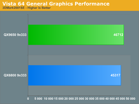
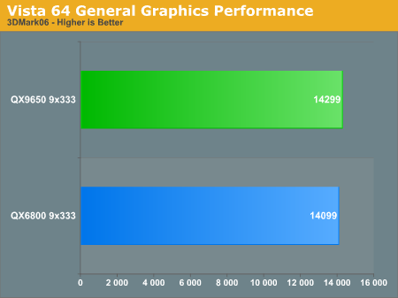
At stock there's little to separate these two processing behemoths from one another. The scores from this motherboard are certainly competitive, falling exactly as we would expect at these clocks.
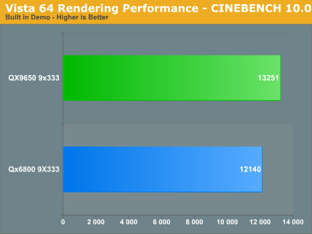
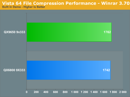
Vista 64-bit - Rendering Performance and WinRAR
For 3D modeling and rendering, we are using the CINEBENCH R10 benchmark. CINEBENCH features two different benchmarks with one test utilizing a single core and the second test highlighting the power of multiple cores in rendering the benchmark image. We utilize the standard multi-core benchmark and default settings. WinRAR's built in benchmark utility is an excellent tool to show overall memory performance and system processing efficiency.
Vista 64-bit - 3D Gaming Performance
We used Company of Heroes, FEAR, and Battlefield 2 to measure 3D graphics performance and in the case of COH complete system processing ability. Our future tests with Vista will feature Crysis and Unreal Tournament 3; both games represent excellent stress testing of both the graphics and processor subsystems.
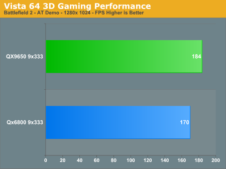
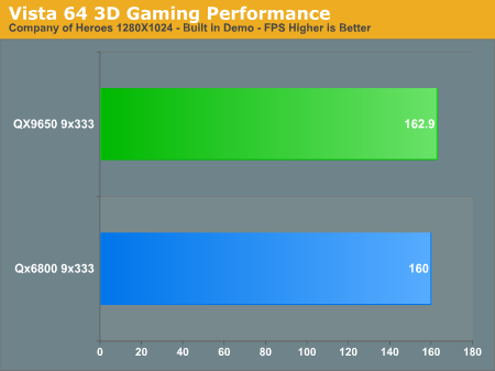
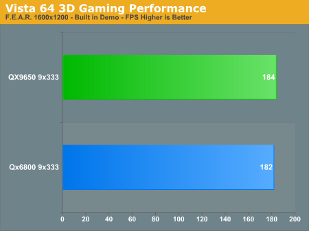
BF2 is the only bench that shows an appreciable difference in performance between using a QX6800 and QX9650. The board's performance is excellent in these benchmarks, as it should be.
Windows XP Benchmarking Results
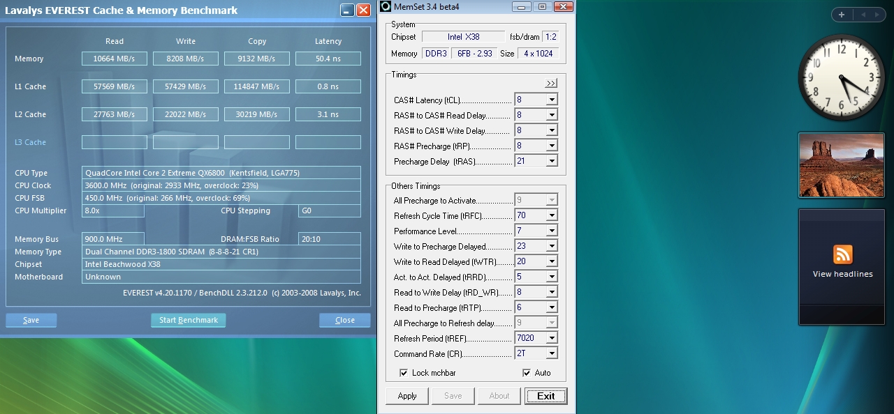
Qx9650 Everest Cache and Memory Benchmark
9x333
 |
9x400
 |
9x450
 |
10x400
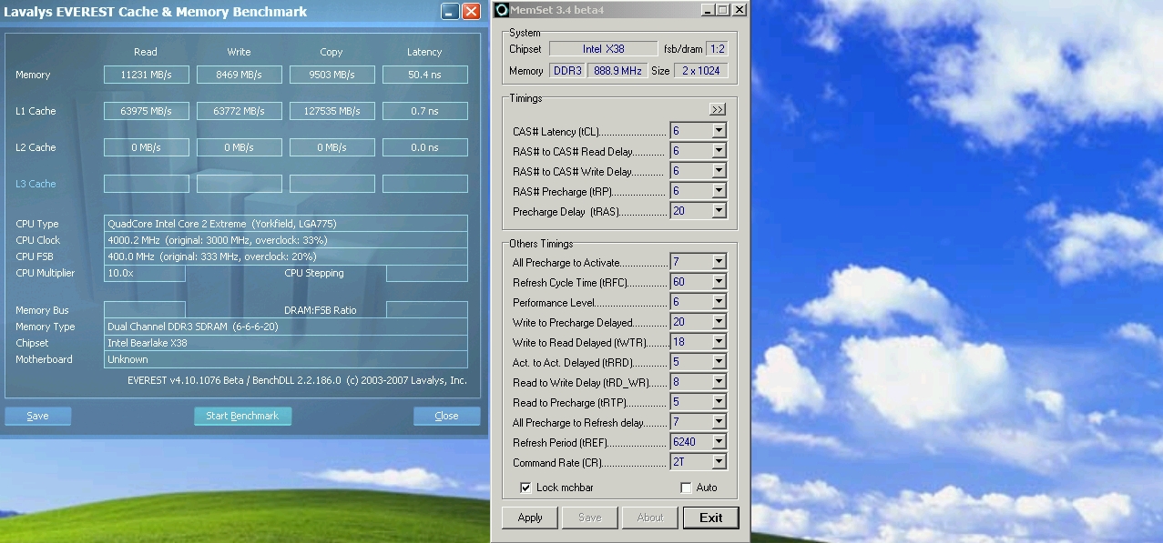 |
One thing that stands out for us is that overall memory access latency is below the figures we have come to expect from DDR3 on the X38/X48 chipset. Although not shown here, this pattern also continues to the 65nm process CPUs. Apart from tRD and the finicky tRD phase shifts (see the BIOS guide later in this review), there are no other chipset registers we can access to easily increase 1N latency performance. We even tried an E6850 to see if increased levels of FSB would allow a linear scaling of memory access latency. Again, the figures were off the pace, coming in around 57ns at 500FSB (3.5GHz) with a tRD of 7. How this pans out into real world benchmark tests is always interesting, especially as most 3D game engines seem ambivalent to overall chipset performance.
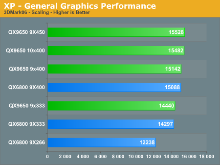
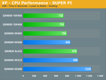
XP Futuremark 3D and Super Pi Benchmarks
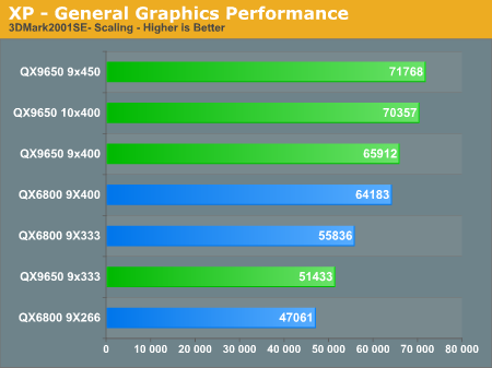
XP Gaming Performance
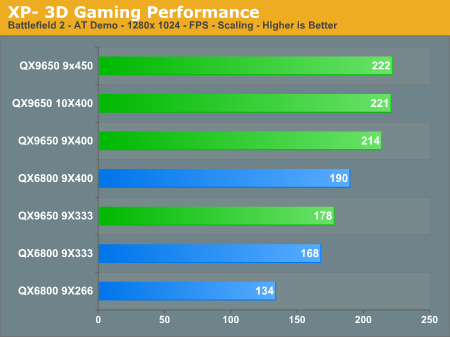

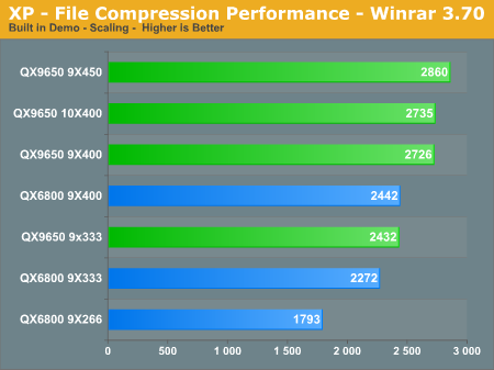
The figures generally speak for themselves, the most striking results are those attained from the Company of Heroes comparison. Higher frame rates over 3.6GHz on either 45nm or 65nm processors are limited by the GPU. In spite of Everest reporting higher memory access latencies than we expected, the benchmark figures are all competitive with most of the other boards we have tested.
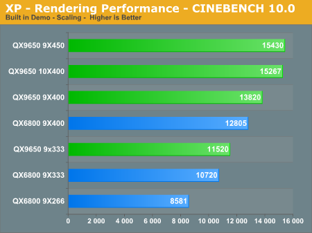
XP 3D Rendering and WinRAR
BIOS Guide and Information
We have picked out a few of the more important BIOS functions for a breakdown of their use. Our testing is all based upon the F3C and F3D BIOS releases, so the ability to use some of these settings may change with future releases.
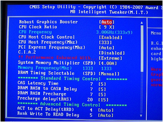
Robust Graphics Booster
Available functions are Auto, Fast and Turbo. We could find no good reason to use anything other than Auto or Turbo mode. Auto seems to default to Turbo mode anyway. In the interest of performance, we did attempt to use the Fast setting, which actually prevented driver initialization during the Windows boot sequence. Sticking on Auto or Turbo is best.
CPU Clock Ratio
This function sets the CPU multiplier; please note the F3D BIOS adds half multiplier support for the QX9650.
CPU Host Clock Control
Options are Enabled and Disabled. Select Enabled to change the FSB and overclock your processor. In the event of a failed overclock this function will return to Disabled.
PCI Express Frequency
Default is Auto. We have found overclocking the PCI-E bus up to 115MHz is possible, although we could not substantiate any real performance advantages in doing so. Speeds over 115MHz are liable to cause non-recognition of SATA drives. Using an IDE drive is recommended if you wish to run over 115MHz.
C.I.A. 2
Gigabyte's automatic overclocking function senses system load and overclocks the processor automatically. There are six available options: Disabled, Cruise, Sports, Racing, Turbo, and Full Thrust. The most aggressive setting is Full Thrust, providing a small percentage CPU/memory overclock under load. Select Disabled for manual overclocking.
Performance Enhanced With
There are three functions available in this setting: Standard, Turbo, and Extreme. Changing this setting does nothing more than manipulate Performance Level (tRD). The Extreme setting selects the default tRD, while Standard and Turbo will relax tRD by 1-2 levels.
System Memory Multiplier (SPD)
Memory divider ratios can be configured by this function. The available memory dividers per Northbridge strap are shown in the table below.
| Gigabyte GA-X48T-DQ6 Available Memory Dividers | |
| Northbridge Strap | Available Memory Dividers |
| 200 MHz | 5:3, 2:1 |
| 266 MHz | 5:4, 3:2, 2:1 |
| 333 MHz | 1:1, 6:5, 8:5, 2:1 |
| 400 MHz | 1:1, 4:3, 5:3, 2:1 |
| . | |
Leaving this function on Auto, results in the 2:1 divider being picked for overclocking by default. For manual use, we found the 333 strap 2:1 divider to be the most stable combination to use for quad-core processors. For dual-core processors, the 266 strap and 3:2 divider worked best for us.
DRAM Timing Selectable (SPD)
If left on Auto the BIOS will attempt to sense and adjust memory timings automatically depending on the level of FSB overclock applied. Set this to manual to obtain control of several key memory/chipset timing parameters below.
CAS
latency Time
DRAM RAS# to CAS# Delay
DRAM RAS# Precharge
Precharge Delay (tRAS)
These are the four primary memory options. If performance is desired, users with 1800MHz DDR3 can aim for 6-6-6-18 1N timings at DDR3-1600 (400FSB 2:1 divider). If low voltages are preferred then either CAS 7-7-6-20 at DDR3-1700 or CAS 8-8-7-21 may be used if you can find enough FSB stability with your processor.
ACT to ACT Delay (tRRD)
Auto will default mainly to a setting of 4 under 500 FSB, which is fine for stability and performance in most cases. Users may wish to experiment with tRRD under 4 via Memset in XP for benchmarking. For high FSB overclocking a setting of 5 may help with stability.
Rank Write to Read Delay
If using manual timings, remember that this setting is offset by -10. Setting 5 manually will give a real setting of 15. The range of interest for overclocking is between 5 and 9 in BIOS (15 to 19 actual), for Micron based modules. Memory speeds over DDR3-1800 require setting of ~9 for stability. For benchmarking, use Memset within Windows for manual tuning.
BIOS - Continued
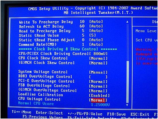
Write To Precharge Delay
Again, this setting is offset by -10. The range of interest in BIOS is between 6 and 13 (16 to 23 actual). Higher numbers mean less performance, but help with stability.
Refresh To Act Delay (aka tRFC)
48-72 is the range of interest, lower settings can have a huge impact on memory bandwidth at the expense fo stability. For benchmarking 48-55 is preferred. For stability testing at high memory speeds start high (72) and work downwards slowly.
Read to Precharge Delay (tRTP)
A setting of 4-6 is usually sufficient across the entire range of FSB and memory speeds that this board offers. 4 is tight and used for benchmarking, while a setting of 5-6 gives stability as FSB and memory speed is scaled. For high FSB speeds with quad-core processors or 4GB memory overclocking a setting of 6 may be preferable.
Static tREAD Value
This setting is more commonly known as Performance Level or tRD and is the most effective chipset performance register available for adjustment on this motherboard. As FSB and memory speed are scaled, tRD and Northbridge voltage will have to be increased to accommodate the additional data throughput. The idea when seeking outright system performance is to run the tightest tRD possible at any given FSB or memory speed. Our retail sample board maxed out at a tRD of 6 at 400 FSB using the 2:1 divider. For 65nm dual core processors, a tRD setting of 7 is usable up to 500FSB. For lower chipset voltages and stability increase tRD by +1 over these figures if stability issues are experienced.
tRD Phase Shift
The user selectable scale runs from 1-31. Setting Auto results in a selection of 0, which means both memory channels remain at the default Performance Level. tRD phase shift allows the user to run either memory channel at a lower Performance Level than the applied BIOS setting of Static tRD Delay. The scale used by Gigabyte is not really intuitive, as it does not immediately show the user which of the memory channel phases are being lowered - at any of the settings available. The number of available or effective phases varies according to the memory divider being used. The explanation of how the phases are configured is outside the scope of this review and deserves a write-up of its own. Look for an upcoming article on AnandTech that will fully describe Intel chipset overclocking in layman terms.
For now, we will stick with the basic rule that a tRD phase adjustment subtracts 1 from the static tRD level at a given point in the FSB/memory read transfer cycle. This function only needs to be used (experimented with) when using FSB speeds that fall between two Performance Level (tRD) FSB limits. Every increase in Performance Level requires a suitable rise in FSB speed to make up the associated memory access latency and bandwidth deficit. If a small hike past a Performance Level limit at a given FSB is made (for additional processor speed), valuable access latency and memory bandwidth is lost unless the rise in FSB speed is very substantial.
With the FSB limits of quad-core processors falling below 470FSB and requiring a tRD of 7-8 in most cases, it can be far easier both in terms of BIOS tuning and board voltages to retain a low tRD of 5 or 6 at around 400FSB using a higher CPU multiplier. The gray area in terms of performance falls between 420-450FSB, where a tRD of 6 starts requiring very high levels of Northbridge voltage to hold steady. When benchmarking with a motherboard there may be instances (due to chipset limitations) where running these intermediate FSBs is the only option. In this instance, it makes sense to apply tRD phase shifts in an attempt to minimize chipset latency loss.
We look at the memory bandwidth and access latency changes at all 31 steps of tRead Phase Adjust below. Please note, the table is for demonstration purposes only; actual board abilities and maximum operating conditions may differ according to a number of variables. We expect that users with quad-core processors will use the 1:2 memory divider at all times, to maximize memory bandwidth at the FSB levels that are available to them. Dual-core CPUs have access to higher stable FSB speeds, in which case using one of the lower dividers to peg memory speed to acceptable and operable speeds will be required.
 |
The rows highlighted in the darker blue represent the most aggressive Phase Adjust points. The table above shows that using the 1:2 memory divider, tRD Phase Adjust settings of 3, 7, 11, 15, 19, 23 (non boot), 27 (non boot), and 30 (non boot) are the most aggressive. In fact, these settings draw an almost complete parallel to running a tRD of 6. To increase FSB potential, some of the less aggressive phase shift settings will need to be used. Again, we stress that most users will not find much to gain in these adjustments. However, for those who are truly passionate about performance tweaking, tRD phase adjustments represent a method of almost linear memory bandwidth and latency scaling throughout the range of chipset capability with a particular CPU. These kinds of tweaks generally bear interest to those who benchmark for maximum scoring potential. Retaining chipset latency can be the difference between a record and tenth place, as there is little to separate overall processor speeds at the top of the Futuremark Orb these days.
We were intrigued by the fact that tRD Phase Shift settings of 23, 27, and 30 would not boot even if we changed Northbridge straps. We managed to get a peek at just how aggressive the non-booting registers were. The Northbridge was set to the 1333 chipset strap with the 1:2 memory divider ratio and 1N command rate at a tRD of 8. We then set a tRD phase shift setting to 23, 27 or 30 and proceeded to boot into Windows. Once Windows had booted up, we lowered the tRD back down to 7 via Memset. The interesting fact is that the board was fully capable of running the Prime95 Torture test at these points for significant periods of time. This points the finger at an inadequate BIOS, rather than a chipset limitation. What is also interesting is that the registers of 23 and 27 are actually more aggressive than running a flat tRD of 6. This implies that these registers may be cross-linked to other hidden chipset performance enhancing registers.
More BIOS Details
Command Rate (CMD)
The options are Auto, 1N and 2N. A setting of 1N can be used almost exclusively while overclocking, bringing a performance advantage of around 2ns to memory access latency. If memory speeds over DDR3-1800 are desired then a setting of 2N may be required for stability.
CPU/PCI-E Clock Driving Control
The default setting is 800mv, with a range of voltage control offered between 700mv-1000mv. As this is a differential amplifier circuit, increasing voltage may actually decrease the clock signal accuracy due to increased power supply noise. Differential circuits are used in preference to single ended circuits because of their noise rejection and low voltage operating capabilities. Increasing voltage to these circuits in turn increases "nasties" such as overshoot and output clock signal jitter. This in turn counteracts the benefits of using a differential amplifier in the first place. We did experiment with various levels of overvoltage and found no gains in stability whatsoever, further cementing our beliefs that more is not always better.
CPU Clock Skew Control and (G)MCH Clock Skew Control
These two clock skew settings are directly related to the voltage control circuit above. They control the PLL output to both the CPU and Northbridge. Again, as a differential amplifier is used, the level of offset required should never exceed 150ps (Pico seconds) of skew to either the CPU or Northbridge reference clocks. At most, PLL circuits such as these should be "good enough" to retain a jitter level of around 150-200ps (lower is better). For those wishing to experiment, adjustments in the range of 0-200ps are of interest for both of the clock skew functions. As a rule, start with the lowest voltage possible, tune either skew setting, and then monitor for effects if any.
DDR3 Overvoltage Control
Base VDimm is 1.5V. The scale offers between 1.5V-3.05V, more than enough to fry any DDR3 modules. 3.05V is certainly more than enough voltage for extreme benchmarking.
PCI-E Overvoltage Control
This sets
a level of overvoltage to the PCI-E bus. The available voltage range is between
1.5V-2.25V. We recommend staying close to stock voltage; higher voltages cause the
board to shut down during the boot cycle. Most modern graphics cards do not benefit
from higher PCI-E voltages. Increasing this voltage will increase noise and magnetic interference into nearby sensitive circuits. Remember, more voltage always has side effects, it is best to let graphics cards draw their power from the PSU PCI/E connectors rather than through the motherboard.
FSB Overvoltage Control
This voltage setting is more commonly known as VTT. Default is 1.10V, with a maximum of 1.41V available. This voltage is critical for quad-core overclocking. 400FSB will require 1.41V right off the bat if stability is desired. (Ed: When isn't that the goal?) Unfortunately, we have no direct control over GTL (Gunning Transceiver Logic) reference values, which are locked at 67% of VTT for CPU die 1 and 63% of VTT for CPU die 2. On a top-end board like this, we had expected to find GTL adjustments, which can be crucial for finding quad-core CPU stability at high FSB speeds.
(G)MCH Overvoltage Control
Default voltage is 1.45V, and the available voltage scale provides an overvoltage of 0.025-0.775V. There an actual undervoltage of 0.2V from the BIOS set overvoltage. For example, as the stock voltage is set to 1.45V a BIOS setting of +0.50V would imply a voltage of 1.95V. However setting +0.50V gives an actual voltage of 1.75V, suggesting an undervoltage of 0.2V.
Loadline Calibration
Setting this to Enabled reduces Intel's specification voltage droop to the CPU when significant power is drawn. Setting enabled places more strain on the PWM circuit and increases voltage overshoot (within the corrective feedback loop) and settling time from load oscillation, which in turn can affect CPU overclock stability. The trade off is that disabling this setting will require a higher Vcore increasing idle CPU temperatures. Vdroop under load is in the region of 0.06V. Therefore, if a full load voltage of 1.35V is required for stability, a setting of 1.41V will be required for Vcore with Loadline Calibration set to Disabled. The Enabled setting gives a Vdroop of around ~0.02V under load. Users are advised to pick a method that suits their cooling, and use common sense to work out how much voltage is safe at idle if Loadline Calibration is set to Disabled.
CPU Voltage
A range from 0.50V to 2.35V is available, making this board suitable for every type of perceivable over and underclocking. Please note we have not experimented with voltages higher than 1.90V with our cascades cooling, so we cannot guarantee voltages over 1.90V actually work.
Final Thoughts on Overclocking
2GB memory overclocking is still proving unreliable between reboots on this board. We have found the board can run a CAS latency of 6 or 7 between 1600-1800MHz. However, the BIOS can be prone to resetting itself between reboots. A CAS setting of 8 is still where this board seems happy for 24/7 operation on current BIOS releases. Dual-core FSB limits are around 500FSB boot-up from BIOS. Using clockgen we have managed speeds of up to 540FSB for benchmarking the board with water-cooling. For absolute stability, we found 495FSB or so is the maximum limit when using a divider that pegs memory speed to around 1600 MHz.
We fully expect these FSB limits to improve with newer BIOS releases. We also made an attempt at 4GB memory overclocking using Microsoft's Vista 64-bit operating system. Using our QX6800 we managed both 6-6-6-18 1N timings at DDR3-1600 and 450FSB DDR3-1800 1N timings that are shown below (please refer to the BIOS templates for actual BIOS settings).
 |
400FSB BIOS Settings
We have decided to provide users with both 400 and 450FSB starting points for quad-core processors. These settings are geared towards a performance oriented setup for 24/7 usage. Individual systems will require stability testing according to personal preferences and component selections. The settings shown are a guideline only; voltages may vary according to individual components and motherboard ability. Remember, perseverance is the key when overclocking!
2GB QX9650 BIOS settings
| Gigabyte GA-X48T-DQ6 Bios Settings @ 400FSB | |
| Robust Graphics Booster | Turbo |
| CPU Clock Ratio | 9x |
| CPU Frequency | 400FSB |
| CPU Host Clock Control | Enabled |
| CPU Host Frequency (MHz) | 400 |
| PCI Express Frequency (MHz) | 100 |
| C.I.A.2 | Disabled |
| Performance Enhanced With | Extreme |
| System Memory Multiplier | 4.00B |
| DRAM Timing Selectable | Manual |
| CAS Latency Time | 6 |
| DRAM RAS# to CAS# Delay | 6 |
| DRAM RAS# Precharge | 6 |
| Precharge delay (tRAS) | 18 |
| ACT to ACT Delay (tRRD) | 4 |
| Rank Write To READ Delay | 7 |
| Write To Precharge Delay | 10 |
| Refresh to ACT Delay | 60 |
| Read to Precharge Delay | 5 |
| Static tRead Value | 6 |
| Static tRead Phase Adjust | Auto |
| Command Rate | 1N |
| CPU/PCIEX Clock Driving | 800mV |
| CPU Clock Skew Control | Normal |
| (G)MCH Clock Skew Control | Normal |
| System Voltage Control | Manual |
| DDR3 Overvoltage Control | (+)0.55 |
| PCI-E Overvoltage Control | Normal |
| FSB Overvoltage Control | (+)0.35 |
| (G)MCH Overvoltage Control | (+)0.25V |
| Loadline Calibration | Disabled |
| CPU Voltage Control | Normal |
If stability issues are experienced with these settings or lower a VDimm is favored, CAS 7-6-6-18 - 1N timings should suffice.
450FSB BIOS Settings
| Gigabyte GA-X48T-DQ6 Bios Settings @ 450FSB | |
| Robust Graphics Booster | Turbo |
| CPU Clock Ratio | 8x (Q6600/QX6800) 9x (QX9650) |
| CPU Frequency | 450FSB |
| CPU Host Clock Control | Enabled |
| CPU Host Frequency (MHz) | 450 |
| PCI Express Frequency (MHz) | 100 |
| C.I.A.2 | Disabled |
| Performance Enhanced With | Extreme |
| System Memory Multiplier | 4.00B |
| DRAM Timing Selectable | Manual |
| CAS Latency Time | 8 |
| DRAM RAS# to CAS# Delay | 8 |
| DRAM RAS# Precharge | 8 |
| Precharge delay (tRAS) | 21 |
| ACT to ACT Delay (tRRD) | 4 |
| Rank Write To READ Delay | 8 |
| Write To Precharge Delay | 12 |
| Refresh to ACT Delay | 60 |
| Read to Precharge Delay | 6 |
| Static tRead Value | 7 or 8 depending on stability requirements (7 = higher performance) |
| Static tRead Phase Adjust | Auto |
| Command Rate | 1N |
| CPU/PCIEX Clock Driving | 800mV |
| CPU Clock Skew Control | Normal |
| (G)MCH Clock Skew Control | Normal |
| System Voltage Control | Manual |
| DDR3 Overvoltage Control | (+)0.55 |
| PCI-E Overvoltage Control | Normal |
| FSB Overvoltage Control | (+)0.35 |
| (G)MCH Overvoltage Control | (+)0.25V |
| Loadline Calibration | Disabled |
| CPU Voltage Control | Dependant on Processor |
Conclusion
Our journey with the GA-48T-DQ6 has been challenging over the last few weeks. Although Gigabyte has been extremely diligent in providing BIOS releases to address our reported problems, we still have not found the everyday overclocking stability we "expected" from this board on any of the beta BIOS releases we have received. This includes cross testing with three separate processor types, all providing varying levels of load to the X48 chipset. What we have found is that basic overclocks that most users will use on this board seem to work at first and then fail at will. For example, using a basic 3.6GHz overclock with any of the newer processors and 400/450FSB, we can boot the motherboard up, play games, surf the web and run stability testing software.
When we go to reboot the board using these previously stable settings, the board greets us with non-boots requiring either a CMOS clear or a complete power-down (until power has drained completely from the board). The board will then reset itself to stock, so that we must re-enter the BIOS and re-apply our previous settings. This is a little disappointing to us at this stage in the game, as Gigabyte has used top-level components in every location on this motherboard. In fact, the engineering behind this board is truly impressive. This shows that using the best hardware is fine, but a solid BIOS is a must if a board is ever to realize its true potential.
We understand it's a little early for a final judgment call, as this board is not yet available in the channel. Thus, we are eager to keep testing the board over the coming weeks to see how things progress. Gigabyte tells us they are working on a new BIOS spin this week, which should address most of the issues we have noticed. In time, we are confident that Gigabyte will deliver this board as the killer product we expect upon delivery to the users - especially when we consider just how good the smaller sibling GA-X38-DQ6 has become with maturity. The GA-X48T-DQ6 has shown us flashes of brilliance, only to let us down when pushed or even nudged into overclock settings that most buyers of this board will try. On the positive side, peripheral compatibility is excellent; we found all ports and expansion slots worked perfectly throughout our testing with a variety of peripherals.
We admire Gigabyte moving forward into the high-end arena; competition is always healthy and helps keep other companies on their toes. We must stress that perseverance prevents us from tossing this board back in the box, meaning we are confident that Gigabyte will have this product fully polished before release. For now though, we would say that at least a few more BIOS spins might be required before we can fully recommend this board to the end-user. A good BIOS will see this board become the product that all X38/X48 boards are judged against. Look out for blog updates as we continue testing new BIOS releases in the coming weeks.


