Original Link: https://www.anandtech.com/show/2180
Gigabyte GA-N680SLI-DQ6: Quad to the Extreme
by Gary Key on February 24, 2007 1:30 AM EST- Posted in
- Motherboards
NVIDIA introduced the 680i chipset back in early November with eager anticipation from users looking to try something different within the Intel processor world. There was a lot of hype, fanfare, and a great deal of media coverage that surrounded the launch of the NVIDIA 600i family of chipsets. We reviewed the 680i chipset in-depth at launch and came away very impressed with the capabilities for the upper-end enthusiast. Since the launch, most of the focus surrounding the 680i chipset changed from its impressive performance and flexibility to problems that seemed to plague the reference board designs from the launch partners such as EVGA and BFG and later on with in-house designs from ASUS and abit. These problems centered on audio issues when using SLI, as well as data corruption or severe performance loss when utilizing SATA drives on the reference boards. The audio issues were solved with a quick BIOS update, although we found in our testing that loading the latest Microsoft DX9 updates helped tremendously. The data corruption on drives was an entirely different issue that seemed to be centered on users with RAID arrays but also spread to single drive users under varying circumstances.
Several BIOS releases later and it seems as if the majority of data corruption issues with the reference boards have been cured. Lucky for us, this was an issue we did not witness in our testing of the ASUS or abit 680i motherboards or with two of our own EVGA motherboards. While NVIDIA attributes these problems to signal timings on the motherboard, we still do not completely understand why the issue occurs on one board and not the other. NVIDIA has commented that statistical variations in the electrical paths between each board can vary, resulting in some boards being affected and others not. We know from the board manufacturers that this chipset is very sensitive to electrical noise and is one of the main reasons why a specific set of voltages is required to reach the upper overclock limits of the board. This specific set of voltage settings seem to differ from board to board and in our initial opinion is based upon having a very "tolerant" MCP. We are almost finished with our testing of several 680i/650i boards and will have a roundup ready in the near future but at this time we commend NVIDIA for their continued persistence in trying to solve these problems.
While it appears the early problems have been solved somewhat, there are still numerous users who are having issues with everything from USB keyboard compatibility to one of our main concerns at this time, quad core overclocking. While overclocking is never guaranteed, paying over $250 for a 680i board that is usually advertised as being designed for the gamer and serious enthusiast with extreme overclocking in mind would lead one to think overclocking would not be a problem. The problems with quad core overclocking on the 680i chipset have been well documented and it appears these problems will be solved shortly, or at least we hope they will be. Enough history; let's discuss the board we are previewing today.
Gigabyte has launched the GA-N680SLI-DQ6 motherboard as of this week. We first discussed this motherboard in early November and then saw a working sample in early December. It has taken Gigabyte some time to get the board launched as they designed it in-house instead of simply reselling the reference board design from NVIDIA. This can be both a positive and a negative depending on how you look at it. One negative is that Gigabyte is late to market, but hopefully the positive is that they learned from the problems surrounding the reference board launch and have something extra to offer the potential buyer looking at a 680i chipset equipped board.
We can definitely say that Gigabyte has something extra to offer on their 680i board. If we were to hold a Pimp my Board contest today, Gigabyte would win without breaking a sweat. This is not meant as a knock against Gigabyte; quite the contrary, they have added just about every feature you possibly can on a motherboard and it all works together. It really works. Their marketing group has been working overtime on figuring every potential way to use the word Quad in front of a feature on the board. We have Quad-Core Optimized, Quad SLI Ready, Quad Gigabit LAN, Quad-Triple Phase, Quad BIOS, and Quad e-SATA features being discussed on the website and product packaging. What really matters in the end is if the board performs well, is stable, has high quality components, and is well supported. We think Gigabyte has met those basic criteria.
This leads us into today's performance preview of the Gigabyte GA-N680SLI-DQ6. In our article today we will briefly go over the board layout and features, provide a few important performance results, and discuss our issues with the board. We will provide a further review of this product and additional performance results in our upcoming roundup. With that said, let's take a look at this board now.
Basic Features
| GIGABYTE GA-N680SLI-DQ6 | |
| Market Segment: | High End Enthusiast - $279.99 |
| CPU Interface: | Socket T (Socket 775) |
| CPU Support: | LGA775-based Pentium 4, Celeron D, Pentium D, Pentium EE, Core 2 Duo, Core 2 Extreme |
| Chipset: | NVIDIA 680i SPP (C55XE) + 680i MCP (MCP55PXE) |
| Bus Speeds: | Auto, 100 to 650 in 1MHz increments |
| Memory Ratios: | Auto, Sync, 1:1, 5:4, 3:2 |
| Memory Speed: | 400MHz~1400MHz in various increments |
| PCIe Speeds: | 100MHz~150MHz in 1MHz Increments |
| Core Voltage: | Auto, 0.68750V to 2.375V in 0.00625V increments |
| FSB Options: | Auto, Linked, Unlinked |
| CPU Clock Multiplier: | Auto, 6x-11x in 1X increments - Core 2 Duo, downwards unlocked Core 2 Extreme 6x-16X |
| DRAM Voltage: | Auto, +025VV ~ +.775V in .025V increments |
| DRAM Timing Control: | Optimal, Expert - 10 DRAM Timing Options |
| NB Voltage: | Auto, +.05V ~ +.20V in .05V increments |
| SB Voltage: | Auto, +.05V ~ +.35V in .05V increments |
| FSB Voltage: | Auto, +.05V ~ +.35V in .05V increments |
| HT Link Voltage: | Auto, +.05V ~ +.35V in .05V increments |
| Memory Slots: | Four 240-pin DDR2 DIMM Slots Dual-Channel Configuration Regular Unbuffered Memory to 8GB Total |
| Expansion Slots: | 2 - PCIe X16 (2-x16 electrical for SLI or Multi-GPU) 1 - PCIe X16 (1-x8 electrical) 1 - PCIe x1 3 - PCI Slot 2.2 |
| Onboard SATA/RAID: | 6 SATA 3Gbps Ports - 680i MCP (RAID 0, 1, 0+1, 5, JBOD) 4 SATA 3Gbps Ports - JMicron JMB363 (RAID 0, 1, 0+1, JBOD) |
| Onboard IDE: | 1 ATA133/100/66 Port (2 drives) - 680i MCP |
| Onboard USB 2.0/IEEE-1394: | 10 USB 2.0 Ports - 4 I/O Panel - 6 via Headers 3 Firewire 400 Ports by TI TSB43AB23 - 1 I/O Panel, 2 via Header |
| Onboard LAN: | Marvell Gigabit Ethernet - PCI Express - 88E1116 PHY - 2 ports via 680i MCP Marvell Gigabit Ethernet - PCI Express - 88E8056 - 1 port Marvell Gigabit Ethernet - PCI Express - 88E8052 - 1 port |
| Onboard Audio: | Realtek ALC888DD - 8-channel HD audio codec |
| Power Connectors: | ATX 24-pin, 8-pin EATX 12V, 4-pin 12V Molex |
| I/O Panel: | 1 x PS/2 Keyboard 1 x PS/2 Mouse 1 x Serial Port 1 x S/PDIF Optical - Out 1 x IEEE 1394a 1 x Audio Panel 4 x RJ45 4 x USB 2.0/1.1 |
| BIOS Revision: | Award F3B |
| Board Revision: | v1.0 |
Gigabyte follows a trend they started in the GA-P965-DQ6 series of boards by offering a significant level of BIOS options for tweaking the board, with emphasis placed on the available memory and voltage settings. In order to reach the majority of these settings you must utilize the archaic Ctrl-F1 keyboard sequence. We figure Gigabyte is still utilizing this keyboard shortcut as they must have paid rights to it, or maybe they are hoping to license it to Apple when they release an iCtrlU device. Whatever the reason, we hope Gigabyte will discontinue its use shortly.
For those who have been using Intel based boards exclusively, Gigabyte displays the FSB speeds in the typical Intel lingo of 100~650MHz instead of the NVIDIA heritage speak of 400~2600 QDR. Our one drawback with the BIOS is the voltages are listed in +{x}V values, which can be confusing if you do not know what the base voltages are for the item selected. We generally found the board would do a very good job of setting the various voltages when Auto was selected until we wanted to go over a 30% overclock. We would then have to chose Manual and adjust the voltages, at times having to do several reboots to lock in the right settings when overclocking. Considering our previous experiences with other 680i boards and knowing what voltage settings generally worked when overclocking, such as 1.45V for FSB, this additional time spent going through a test trial was somewhat frustrating.
The board is fully featured and looks to be hunting bear when it comes to the option check off list. We believe the majority of additional features like the two extra LAN ports and four additional SATA ports would make this an ideal board for home/multimedia/office/gaming server. It would also work well as the center piece for a gaming system where storage, expansion slots, and networking are a priority over pure overclocking performance. The Realtek ALC-888DD offers full Dolby Digital Live and DTS connect support and Gigabyte tossed in IEEE-1394 support as well. With the included external cables you also have the choice of up to four e-SATA ports depending upon your drive configuration.
Gigabyte also includes a full suite of utilities for the board: EasyTune5, Download Center, Xpress Install, @BIOS, and Xpress BIOS Rescue. We found the @BIOS utility to be very handy for downloading and then updating the BIOS while in Windows. For those who are squeamish about updating their BIOS within Windows, Gigabyte has their Q-Flash utility built into the BIOS that allows updating from a floppy drive. Now we just need the ability to update from a USB flash memory drive instead.
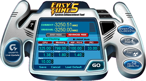
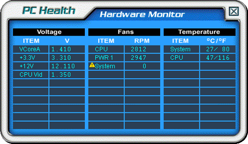
EasyTune5 is probably one of the most useful utilities in the Gigabyte arsenal and allows for control of the FSB and certain voltages within Windows. We found the utility worked well for squeezing out those last few FSB increases, but we still found ourselves tweaking the BIOS the majority of the time. The PC Health monitor provided basic readings of the system temperatures along with voltages. The board offers limited support for the NVIDIA nTune utility that limited changes to certain memory settings and FSB rates only.
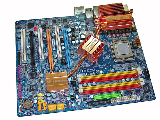
Board Layout and Features
 |
| Click to enlarge |
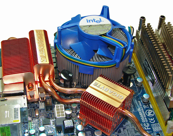
Gigabyte did a really nice job with the layout of this board considering all of the options provided. The color combination continues Gigabyte's recent design trend and is a little over the top for us, but it's not as bad as the more garish color schemes we have seen in the past on other boards. The board was easy to install in our Cooler Master CM Stacker 830 although we recommend installing your air cooler first due to the cramped quarters around the CPU area.
Unfortunately, the location of the 8-pin ATX connector near the CPU area caused cable management issues with a variety of air coolers. We also had trouble attaching our fan cable to the fan header located right under the upper lip of the Silent-Pipe heatsink system installed over the mosfets. The board features a total of four fan headers (two four-pin, two three-pin) with three that are controlled via the BIOS. A fifth one would have been preferred on the far left side of the board. The board features a quad three-phase voltage regulator system and 100% use of Conductive Polymer Aluminum Solid Capacitors that provided superb stability throughout testing.
Click for Additional View
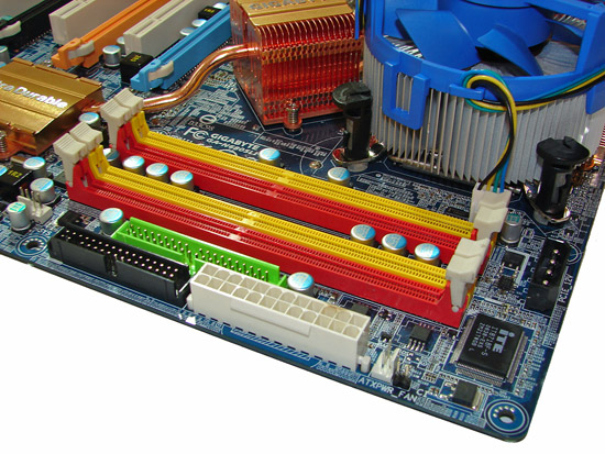
The DIMM module slots' color coordination is correct for dual channel setup based upon the premise of installing DIMMs in the same colored slots for dual-channel operation. It was very easy to install memory modules with a full size video card placed in the first PCI Express x16 slot. Gigabyte places the CPU fan header above the first DIMM slot and it is an easy reach for most CPU fan/heatsink cables. The 24-pin ATX connector, black floppy connector, and the green IDE port connector are located below the DIMM slots along the edge of the board.
We would have preferred the IDE and floppy connectors being reversed as threading the IDE cable over the power cable with the fourth DIMM slot occupied was not a pleasant experience once the board was in the case. In fact, we just wish the floppy connector would have disappeared altogether. The 4-pin 12V Molex connector that is required for SLI operation is located on the far right hand side of the board.
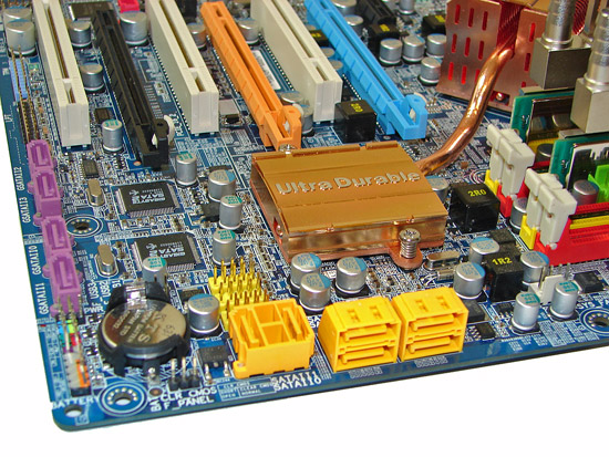
The six nForce 680i SATA ports are yellow and are conveniently located below the 680i MCP. The SATA ports feature the newer clamp and latch design. We found the positioning of the SATA ports to be very good when utilizing the any of the expansion slots, although we had to bend our SATA cable a little when using the first port with a NVIDIA 8800GTX . The MCP is passively cooled and remained hot to the touch throughout testing. The chassis panel and battery are located on the lower left edge of the board along with a two-pin clear CMOS header. The four JMicron JMB363 SATA ports are pink and located along the left edge of the board. We had to use special right angled flat head SATA cables when our second 8800GTX was installed; otherwise the ports are basically blocked.
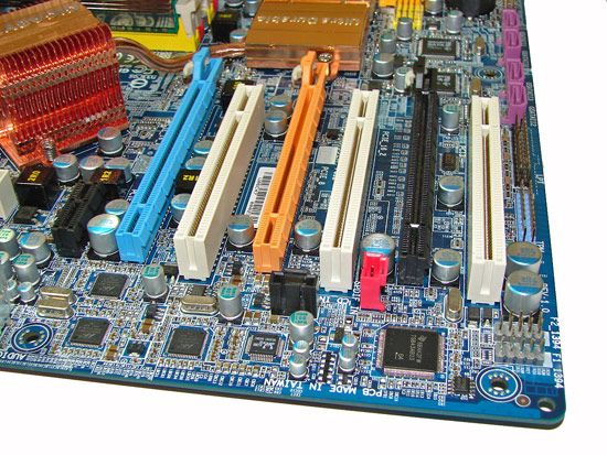
The board comes with three physical PCI Express x16 connectors (2x16 electrical, 1x8 electrical), one PCI Express x1, and three PCI 2.2 connectors. The layout of this design offers one of the better triple x16 connector designs we have worked with to date. However, the first and third PCI slots will be unavailable if you utilize graphics cards with dual slot cooling solutions.
Click for Additional View
Getting back to CPU socket area, we find a limited amount of room for alternative cooling solutions. We utilized the stock heatsink/fan in our normal testing but also verified a few larger Socket-775 air cooling solutions would fit in this area during our overclocking tests. It was difficult routing the 8-pin ATX power cable with a cooling solution like the Tuniq Tower 120 installed. Our Tuniq 120 and Scythe Infinity coolers fit but had to be oriented in a single position.
The 680i SPP is passively cooled with a mid-rise heatsink unit that did not directly interfere with any installed peripherals or heatsinks. We found the Silent-Pipe heatsink system that Gigabyte designed proved to work quite well during overclock testing with our particular case and cooling system. However, those wanting to run the board at its maximum OC on a 24/7 basis will need additional fan cooling over the heatsinks at all times. The 680i chipset is like a mini-furnace when overclocked.
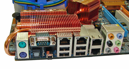
The rear panel contains the standard PS/2 mouse and keyboard ports, serial port, and four USB 2.0 ports. The two nForce 680i LAN (RJ-45) ports have two LED indicators representing Activity and Speed of the connection. The two Marvell Gigabit PCI-E LAN ports are located between the LAN/USB and Audio ports. The audio panel consists of 6 ports that can be configured for 2, 4, 6, and 8-channel audio connections for the Realtek ALC 888DD HD codec, along with an S/PDIF optical out port.
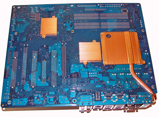
The back of the board contains Gigabyte's exclusive CrazyCool 2 system that is designed to help dissipate heat from the CPU and chipset areas. We could not tell in subjective testing with this system installed if it worked or not. However, the scientific data that Gigabyte provided does support their temperature reduction claims. If you remove the main CPU plate it requires the removal of the heatsink located over the I/O panel. We found this was the best way to properly mount the Tuniq 120 or other coolers with large back plates.
Dual Core Overclocking
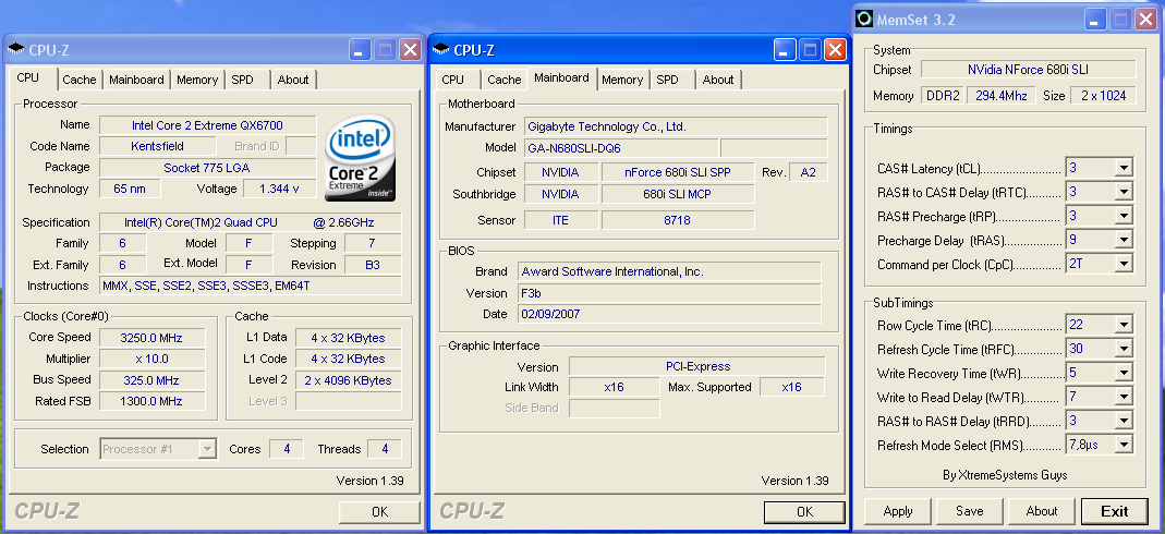
| GIGABYTE GA-N680SLI-DQ6 Dual Core Overclocking Testbed |
|
| Processor: | Intel Core 2 Duo E6600 Dual Core, 2.4GHz, 4MB Unified Cache 1066FSB, 9x Multiplier |
| CPU Voltage: | 1.4875V (default 1.3250V) |
| Cooling: | Tuniq 120 Air Cooling |
| Power Supply: | OCZ ProXStream 1000W |
| Memory: | OCZ Flex XLC (2x1GB) (Micron Memory Chips) OCZ Flex XLC PC2-6400 (ProMOS Memory Chips) |
| Video Cards: | 1 x MSI 8800GTX |
| Hard Drive: | Western Digital 150GB 10, 000RPM SATA 16MB Buffer |
| Case: | Cooler Master CM Stacker 830 |
| Maximum CPU OC: | 440x9 (3-4-4-9 1T, 880MHz, 2.375V), CPU 1.4875V 3960MHz (+65%) |
| Maximum FSB OC: | 490x7 (3-4-4-15 2T, 800MHz, 2.275V), CPU 1.4500V 3430MHz (+84% FSB) |
| . | |
 |
| Click to enlarge |
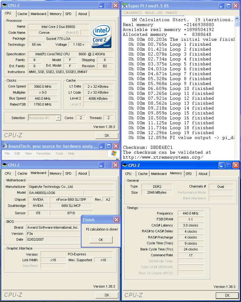
We were easily able to reach a final benchmark stable setting of 9x440 FSB resulting in a clock speed of 3960MHz. We were able to run our OCZ Flex PC2-9200 and our Corsair PC2-6400C3 at the reported timings with 1T Command Rate enabled. The shipping F2 BIOS limited us to a 9x425 setting and a 2T Command Rate. The latest F3B beta BIOS that greatly improved our quad core overclocks but limited us to a 9x430FSB setting; it also allowed 1T Command Rates at DDR2-860. Vdroop was acceptable on this board during overclocking with an average drop of .02 ~.03V during load testing.
We also tested our new OCZ Flex PC2-6400 and G.Skill F2-6400CL4D-2GBHK memory based on the ProMOS IC chips with great success. The OCZ Flex PC2-6400 was able to run at DDR2-880 (9x440) speed with timings at 3-4-4-15 2T at 2.275V and the G.Skill F2-6400CL4D at 4-4-4-8 2T at 2.250V. The balance of the memory timings were set to Auto as the BIOS was very temperamental when manually setting the timings.
 |
| Click to enlarge |
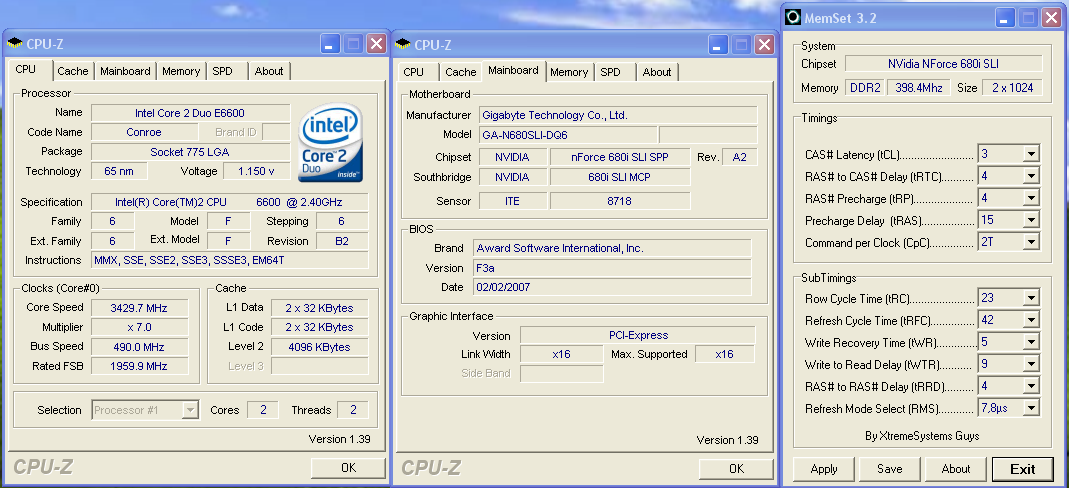
We dropped the multiplier on our E6600 to seven and were able to reach 490 FSB without issue on the F3A BIOS. We were able to enter XP at 7x510 and the board would POST at 7x514. However, at least with our sample, stability over 500 FSB dropped off quickly and we feel like this BIOS release was designed with a 500FSB in mind but not much more. The F3B BIOS proved to be stable at 503 FSB and would POST at 7x518 but memory timings had to be backed off when compared to the F3A BIOS at both the DDR2-800 unlinked or DDR2-1006 synced speeds. The shipping F2 BIOS limited us to a final 7X468 setting with the same memory timings utilized in our F3A testing.
Quad Core Overclocking
| GIGABYTE GA-N680SLI-DQ6 Quad Core Overclocking Testbed |
|
| Processor: | Intel Core 2 Extreme QX6700 Quad Core, 2.66GHz, 8MB Unified Cache 1066FSB, 9x Multiplier |
| CPU Voltage: | 1.3625V (default 1.3500V) |
| Cooling: | Tuniq 120 Air Cooling |
| Power Supply: | OCZ ProXStream 1000W |
| Memory: | OCZ Flex XLC (2x1GB) (Micron Memory Chips) |
| Video Cards: | 1 x MSI 8800GTX |
| Hard Drive: | Western Digital 150GB 10, 000RPM SATA 16MB Buffer |
| Case: | Cooler Master CM Stacker 830 |
| Maximum OC: | 325x10 (3-3-3-9 2T, 800MHz, 2.325V), CPU 1.3625V 3250MHz (+22%) |
| . | |
 |
| Click to enlarge |
Needless to say, quad core overclocking on the 680i platforms have not been spectacular and downright worrisome, considering that we have not been able to reach a stable 333FSB with any 680i board until ASUS released their 1002 BIOS for the Striker Extreme last week. We understand EVGA will be releasing a fix for their reference board design shortly so maybe the problems will be solved. In the meantime, if you are looking for high FSB overclocks with your quad core then look at the Intel P965 or AMD RD600 chipsets.
We dropped the multiplier on our QX6700 and were unable to improve upon the same 325 FSB level at the stock 10x multiplier. The board would not even POST past a 340FSB and we could enter XP at 332FSB, but it was only good for a screenshot session. We required the F3B BIOS to reach our final benchmark stable 325FSB setting as the F3A was not stable above 312 and the shipping F2 BIOS topped out at 304. Although the board is touted as being "Quad-Core optimized", we did not see it. Gigabyte engineering is working to address this shortcoming, although if it is being caused by the chipset itself they may not have much success. We will continue to monitor the situation for now.
Test Setup
| Standard Test Bed Performance Test Configuration |
|
| Processor: | Intel Core 2 Duo E6600 (2.4GHz, 4MB Unified Cache) Intel Core 2 Extreme QX6700 (2.66GHz, 8MB Unified Cache) |
| RAM: | OCZ Flex XLC (2x1GB), 2.30V (Micron Memory Chips) |
| Hard Drive: | Western Digital 150GB 10, 000RPM SATA 16MB Buffer |
| System Platform Drivers: | Intel - 8.1.1.1010 NVIDIA - 9.35, 8.43 ATI - 6.10 |
| Video Cards: | 1 x MSI 8800GTX |
| Video Drivers: | NVIDIA 97.92 |
| CPU Cooling: | Tuniq 120 |
| Power Supply: | OCZ ProXStream 1000W |
| Optical Drive: | Plextor PX-760A |
| Case: | Cooler Master CM Stacker 830 |
| Motherboards: | ASUS Striker Extreme (NVIDIA 680i) - BIOS 1002 ASUS P5N-E SLI (NVIDIA 650i) - BIOS 0401 ASUS P5B-E (Intel P965) - BIOS 0402 B06 DFI LANParty UT ICFX3200-T2R/G (AMD RD600) - BIOS 12/22 GIGABYTE GA-N680SLI-DQ6 - BIOS F3B/F3A Intel D975XBX2 (Intel 975X) - BIOS 2333 |
| Operating System: | Windows XP Professional SP2 |
| . | |
A 2GB memory configuration is now standard in the AT test bed as most enthusiasts are currently purchasing this amount of memory. Our choice of high-end OCZ Flex XLC memory from OCZ offered a very wide range of memory settings during our stock and overclocked test runs. We also utilized our Corsair XMS2 Dominator (Twin2x2048-9136C5D) memory on this board to verify DDR2-1066 compatibility with another memory type. We are currently completing testing several other memory modules ranging from TwinMOS and WINTEC DDR2-800 down to A-DATA DDR2-533 for compatibility and performance benchmarks in our next article. We will also be looking at 4GB memory compatibility in future motherboard articles. Our memory timings are set based upon determining the best memory bandwidth via MemTest 86 and test application results for each board. We only optimize the four main memory settings with sub-timings remaining at Auto settings.
We are utilizing an MSI 8800GTX video card to ensure our 1280x1024 resolutions are not completely GPU bound for our motherboard test results. We did find in testing that applying a 4xAA/8xAF setting in some of today's latest games created a situation where the performance of the system starts becoming GPU limited, but compared to previous X1950 XTX testing we should have quite a bit more GPU headroom now. Our video tests are run at 1280x1024 resolution for this article at High Quality settings. We also tested at 1600x1200 and 1920x1200 4xAA/8xAF for our NVIDIA SLI results that will be presented in our upcoming 680/650i roundup.
All of our tests are run in an enclosed case with a dual optical/hard drive setup to reflect a moderately loaded system platform. Windows XP SP2 is fully updated and we load a clean drive image for each system to ensure driver conflicts are kept to a minimum.
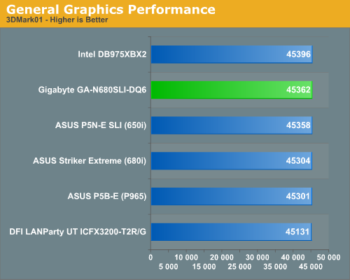
Synthetic Graphics Performance
The 3DMark series of benchmarks developed and provided by Futuremark are among the most widely used tools for benchmark reporting and comparisons. Although the benchmarks are very useful for providing apple to apple comparisons across a broad array of GPU and CPU configurations they are not a substitute for actual application and gaming benchmarks. In this sense we consider the 3DMark benchmarks to be purely synthetic in nature but still very valuable for providing consistent measurements of performance.
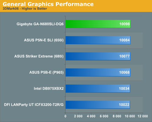
In our 3DMark06 test, each platform score is basically the same although we see the DFI RD600 based motherboard trailing slightly. We attribute this to the latest released BIOS that has generated slightly lower performance results than our original test beta.
In the more memory and CPU sensitive 3DMark01 benchmark we see the Intel 975X board pulling away from the other boards due to its superior memory bandwidth at stock settings. Even though this holds true to some degree for the ASUS P5B-E based on the P965 chipset, we see it scoring slightly lower than our NVIDIA solutions due to relaxed MCH timings that allow it to excel in high FSB overclocking.
Although our Sandra memory bandwidth scores along with Memtest86 testing consistently show the RD600 performing slightly better than the 680i or 650i, but our 3D01 benchmark is not showing this advantage. NVIDIA based chipsets perform very well in graphics tests and the scores from our Intel DB975XBX2 indicate a highly tuned platform.
General System Performance
The PCMark05 benchmark developed and provided by Futuremark was designed for determining overall system performance for the typical home computing user. This tool provides both system and component level benchmarking results utilizing subsets of real world applications or programs. This benchmark is useful for providing comparative results across a broad array of GPU, CPU, Hard Disk, and Memory configurations along with multithreading results. In this sense we consider the PCMark benchmark to be both synthetic and real world in nature, and it provides consistency in our benchmark results.
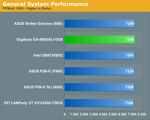
The Gigabyte 680i is very competitive in this benchmark although we expected slightly better performance based upon our application results. The 650i and 680i chipsets scored very well on the single task disk benchmarks and both performed almost equally on the graphics subsystem tests where they led the field. However, our 975X and P965 chipset boards won the multi-tasking tests while the RD600 finished in the middle on most of the tests.
General System Performance
We devised a script that would compress our standard test folder consisting of 444 files, ten subfolders, and 602MB worth of data, convert a 137MB High Definition QuickTime movie clip to a 37MB MPEG-4 format, play back the first two chapters of Office Space with PowerDVD, and run our AVG anti-virus program in the background. We stop the script when the file compression and video conversion are complete. This is a very taxing script for the CPU, Memory, and Storage subsystem. We also found it to be a good indicator of system stability during our overclocking testing.
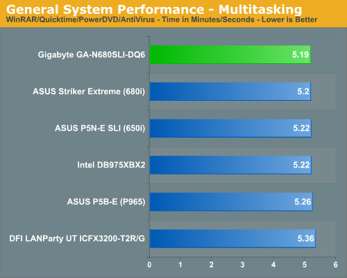
The performance difference basically mirrors our PCMark 2005 tests with the 680i boards finishing first due to great disk performance, although the Intel chipsets consistently completed the QuickTime conversion first. The DFI RD600 board scores last although it generated the best video playback results. We also noticed it would stutter at times when converting the QuickTime file.
Media Encoding Performance
Our first encoding test is quite easy - we take our original Office Space DVD and use AnyDVD Ripper to copy the full DVD to the hard drive without compression, thus providing an almost exact duplicate of the DVD. We then fire up Nero Recode 2, select our Office Space copy on the hard drive, and perform a shrink operation to allow the entire movie along with extras to fit on a single 4.5GB DVD disc. We leave all options on their defaults except we disable the advanced analysis option. The scores reported include the full encoding process and are represented in minutes and seconds, with lower numbers indicating better performance.
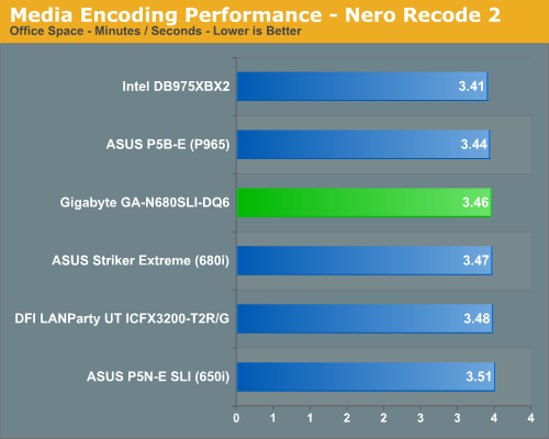
We continue to see a strong performance from the Intel 975X in our application tests. In previous testing our ASUS 650i and 680i boards were almost two minutes slower in this test as we consistently found the performance of the 680i/650i to be lacking due to disk access issues. The conversion process would consistently slow down while the disk was being accessed. The quality of the video conversion was never affected but it appeared under heavy CPU usage that disk performance suffered. After the latest round of BIOS and driver updates these two boards now score close to the other chipsets.
Audio Encoding Performance
While the media encoding prowess of the P965 boards were superb in our initial media encoding testing, we wanted to see how they faired on the audio side. Our audio test suite consists of Exact Audio Copy v095.b4 and LAME 3.98a3. We utilize the INXS Greatest Hits CD that contains 16 tracks totaling 606MB of one time '80s hits.
We set up EAC for variable bit rate encoding, burst mode for extraction, use external program for compression, and to start the external compressor upon extraction (EAC will read the next track while LAME is working on the previous track, thus removing a potential bottleneck with the optical drive). We also set the number of active threads to two to ensure both cores are active during testing. The results are presented in minutes/seconds for the encoding process, with lower numbers being better.
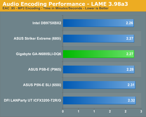
As in the media encoding section, the more intensive CPU and storage system tests seem to favor the 975X over the P965/NV650i/RD600 when running at the same memory timings. Our two 680i boards are right on the heels of the 975X board with all scores being extremely close. Our Plextor drive consistently took two minutes and nine seconds to read all sixteen tracks. This means our test systems are only utilizing one core during testing until the midway point of the extraction process where the drive speed was exceeding the capability of the encoder and required the use of a second thread.
File Compression Performance
In order to save space on our hard drives and ensure we had another CPU crunching utility, we will be reporting our file compression results with the latest version of WinRAR that fully supports multi-treaded operations and should be of particular interest for those users with dual core or multi-core systems. Our series of file compression tests utilizes WinRAR 3.62 to compress our test folder that contains 444 files, ten subfolders, and 602MB worth of data. All default settings are utilized in WinRAR along with our hard drive being defragmented before each test.
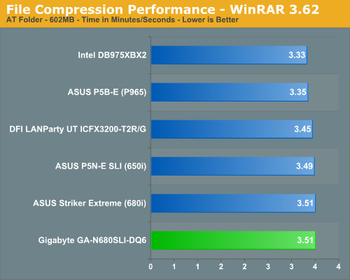
In a complete reversal of the other application results we see our 680i boards finishing last. We see the Intel P965 and 975X chipsets leading once again as both seem to thrive in CPU intensive tasks. The DFI RD600 board continues to finish in the middle of the pack.
Standard Gaming Performance
As usual, gaming performance was tested with a variety of current games. We ran benchmarks with our standard 1280x1024 resolution without antialiasing enabled (and generally without anisotropic filtering, though that varies by game). Given the number of users that run 19" LCDs these days, 1280x1024 represents one of the most commonly used resolutions. We could certainly increase the amount of eye candy being displayed in most of the games, but as this is a motherboard benchmark we aren't particularly interested in maxing out the graphics cards in our tests.
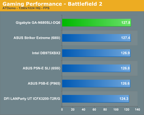
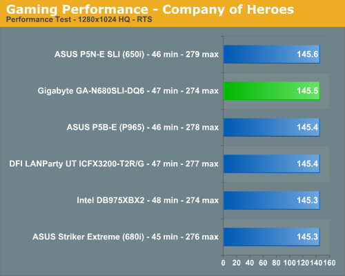
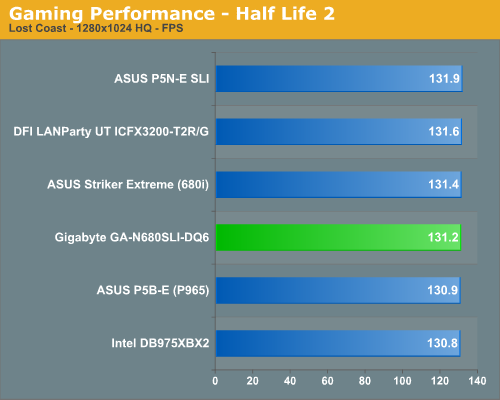
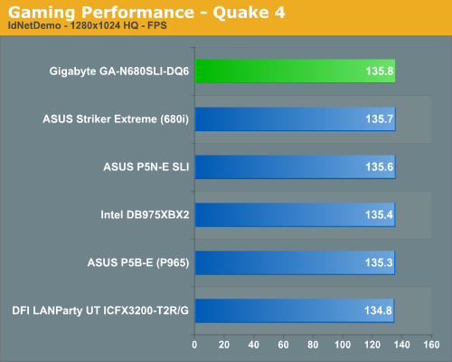
It's the same old song and dance but these results basically show that any of the chipsets listed will perform equally in today's games when equipped with the same GPU. We did not experience any issues during testing or during game play with the Gigabyte board. We generally play every game for at least a couple of hours on each board to ensure there are no issues such as overheating, stuttering, or network problems when playing on-line with various combinations of components.
Disk Controller Performance
The AnandTech iPeak test is designed to measure "pure" hard disk controller performance, and in this case, we keep the hard drive as consistent as possible while varying the hard drive controller. The idea is to measure the performance of each hard drive controller with the same hard drive.
We played back our raw files that are recorded I/O operations when running a real world benchmark - the entire Winstone 2004 suite. Intel's iPeak utility was then used to play back the trace file of all I/O operations that took place during a single run of Business Winstone 2004 and MCC Winstone 2004. To try to isolate performance differences to the controllers that we are testing we are using the Western Digital 74GB Raptor with 16MB cache for both our standard disk controller and RAID performance tests for this article. The drive is formatted before each test run and a composite average of three tests on each controller interface is tabulated in order to ensure consistency in the benchmark.
iPeak gives a mean service time in milliseconds; in other words, the average time that each drive took to fulfill each I/O operation. In order to make the data more understandable, we report the scores as an average number of I/O operations per second so that higher scores translate into better performance. This number is meaningless as far as hard disk performance is concerned, as it is just the number of I/O operations completed in a second. However, the scores are useful for comparing "pure" performance of the storage controllers in this case.
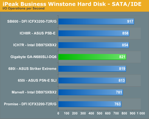
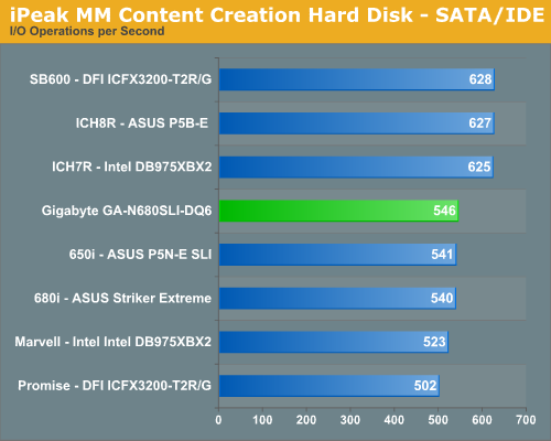
The performance patterns hold steady across both Multimedia Content I/O and Business I/O with the SB600 outperforming the Intel ICH7R, Intel ICH8R, and NVIDIA 680i/650i chipsets in our non-Raid tests. The Promise controller on the DFI board is the slowest of all solutions with the Marvell controller on the Intel 975X performing only slightly better. The 680i and 650i MCP units are different but their disk performance in our tests is basically alike. We also ran RAID 0 and RAID 5 tests on each controller with the results being in favor of the 680i MCP by around 2%. We did not witness any data corruption on either ASUS NVIDIA based board as has been reported on the 680i reference boards, and we consider this problem to be fixed since our P23 BIOS update. We did have data corruption issues with the Gigabyte board when using 1T Command Rate at DDR2-800 with an early F2 beta BIOS. This problem did not occur when using 2T Command Rate and has not been evident in our testing with the F3 BIOS.
Overclocking
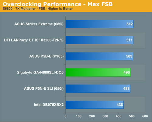
As we mentioned earlier in the article, the overclocking capability of the Gigabyte board has varied widely with each BIOS release we have received. This will be disappointing to some users and we expected a little better overclocking capability based upon the quality of the board and its BIOS options. However, until Gigabyte completes the F3 BIOS tuning we will withhold our final judgment. One area we found interesting is the board did not experience the same number of FSB holes that we have seen on the reference boards. We did not experience the typical FSB hole around 416~423FSB but apparently hit one right around 480 in the latest beta BIOS. We also found that during overclocking we had to set our memory voltages a little higher than on the other boards to attain the same timings. We have experienced this before with the DS3 boards and it was due to tighter sub-timings in order to slightly improve the performance of the board.
First Impressions
There you have it: a first glimpse at a very interesting board that tries to be everything to everyone with just about every possible option you could logically fit on a board. We were impressed that all of the options worked as advertised and we actually have the board running Vista Ultimate x64 without an issue at this time. Whether there is a user base that needs a board with Quad Gigabit LAN and ten SATA ports is open for debate but our hats are off to Gigabyte for getting all of the various options to work together.
The performance of the board is very solid but considering the time it took to get to market we did expect slightly better performance and a more polished BIOS. After several weeks of stability and compatibility testing with a wide range of components we did not find too many issues with our early release board. The majority of the problems we did find were immediately fixed by Gigabyte. Hopefully, Gigabyte will provide us with a released F3 BIOS shortly that addresses a few remaining issues.
You might ask what those issues are since we did not provide a full in-depth review of each option on this board in our preview. Our first issue deals with memory performance. This board does not like 1T Command Rates at DDR2-800; we have not had this issue on the ASUS boards and luckily our EVGA reference board seems to like 1T operation also. We had numerous issues when 1T was working correctly at DDR2-800 that ranged from data corruption to random shutdowns. This has been fixed since the F3A BIOS but now we have to overclock the memory past DDR2-811 to get 1T operation - this is more like an annoyance than a real problem, but it still needs to be addressed. At least on the F3A BIOS we found 1T operation was very stable from DDR2-811 to DDR2-880 with our high end memory from OCZ and Corsair. This is not the case with the F3B BIOS or the shipping F2 BIOS when utilizing 1GB modules. While performance might only vary up to 3% with 1T enabled, it is still a choice we would like to have after shelling out over $279 for the board.
Our next issue is the lack of viable overclocking with our quad core processors. While most people would not be too worried about this or might simply raise the multiplier to reach high CPU speeds with the QX6700, we consider it to be a problem when the boards will not reach at least 333FSB. The reason for this is that the upcoming 1333FSB (Quad Pumped) quad core processors will require the 333FSB base. When these hit the market we have to wonder if these boards will perform as advertised. The E6850 (1333FSB Dual Core) works without an issue on this board and we understand the new quad cores will also, but it has been almost four months since the release of the 680i chipset and we are still seeing this problem.
Fortunately, some of the early issues that plagued the reference boards are not present on this particular board and beta BIOS. We had no issues enabling RAID, SLI, and using the on-board Realtek ALC-888DD codec together. We are still not fond of the EAX compatibility and audio quality of the Realtek HD codecs as the ADI chipsets simply sound better. More importantly, they correctly generate EAX 2.0 audio streams and overall have slightly better audio quality. However, if you are a serious gamer or audiophile you will likely already have a discrete sound card, making audio concerns something of a moot point.
We still have significant testing left to complete on our new retail kit but at this time we like the progress the 680i chipset has made as well as Gigabyte's implementation. The performance of this early production board has been very good and stability has not been a real issue until the board was at or near its limits - limits that probably will not satisfy the extreme computer enthusiast but should be enough for the majority of potential owners.
We can say the additional features such as Quad Gigabit Ethernet, SLI combined with our AGEIA physics card, RAID capability on the additional four SATA 3Gb/s ports via the two JMicron JMB363 chipsets, and enhancements like LinkBoost, SLI Ready Memory, and IEEE-1394 all work as advertised. We found memory compatibility was greatly improved from previous Gigabyte releases as our ProMOS and Elpida modules worked fine. We would like to see some additional memory and overclocking performance tuning completed by Gigabyte but overall the BIOS releases are very solid if not spectacular.
We think the Gigabyte GA-N680SLI-DQ6 has a bright future in the enthusiast performance market based upon solid performance, an incredible amount of features, and more importantly the support we expect Gigabyte to provide to the owners of this board. It might not ever be the best performing 680i board but no one can question it beats all other boards when it comes time to roll out the bling-bling.


