Original Link: https://www.anandtech.com/show/21469/amd-details-ryzen-ai-300-series-for-mobile-strix-point-with-rdna-35-igpu-xdna-2-npu
The AMD Zen 5 Microarchitecture: Powering Ryzen AI 300 Series For Mobile and Ryzen 9000 for Desktop
by Gavin Bonshor on July 15, 2024 9:00 AM EST- Posted in
- CPUs
- AMD
- Mobile
- Zen 5
- AM5
- XDNA 2
- Ryzen 9000
- Ryzen AI 300
- RDNA 3.5
- Radeon 890M
Back at Computex 2024, AMD unveiled their highly anticipated Zen 5 CPU microarchitecture during AMD CEO Dr. Lisa Su's opening keynote. AMD announced not one but two new client platforms that will utilize the latest Zen 5 cores. This includes AMD's latest AI PC-focused chip family for the laptop market, the Ryzen AI 300 series. In comparison, the Ryzen 9000 series caters to the desktop market, which uses the preexisting AM5 platform.
Built around the new Zen 5 CPU microarchitecture with some fundamental improvements to both graphics and AI performance, the Ryzen AI 300 series, code-named Strix Point, is set to deliver improvements in several areas. The Ryzen AI 300 series looks set to add another footnote in the march towards the AI PC with its mobile SoC featuring a new XDNA 2 NPU, from which AMD promises 50 TOPS of performance. AMD has also upgraded the integrated graphics with the RDNA 3.5, which is designed to replace the last generation of RDNA 3 mobile graphics, for better performance in games than we've seen before.
Further to this, during AMD's recent Tech Day last week, AMD disclosed some of the technical details regarding Zen 5, which also covers a number of key elements under the hood on both the Ryzen AI 300 and the Ryzen 9000 series. On paper, the Zen 5 architecture looks quite a big step up compared to Zen 4, with the key component driving Zen 5 forward through higher instructions per cycle than its predecessor, which is something AMD has managed to do consistently from Zen to Zen 2, Zen 3, Zen 4, and now Zen 5.
AMD Zen 5 Microarchitecture: 16% Better IPC Than Zen 4
Both the AMD Ryzen AI 300 series for mobile and the Ryzen 9000 series for desktops are powered by AMD's latest Zen 5 architecture, which brings a host of improvements in performance and efficiency. Perhaps the biggest improvement within their mobile lineup is the integration of the XDNA 2 NPU, which is designed to make use of the Microsoft Copilot+ AI software. These new mobile processors via the NPU can deliver up to 50 TOPS of AI performance, making them a significant upgrade in AMD's mobile chip lineup.
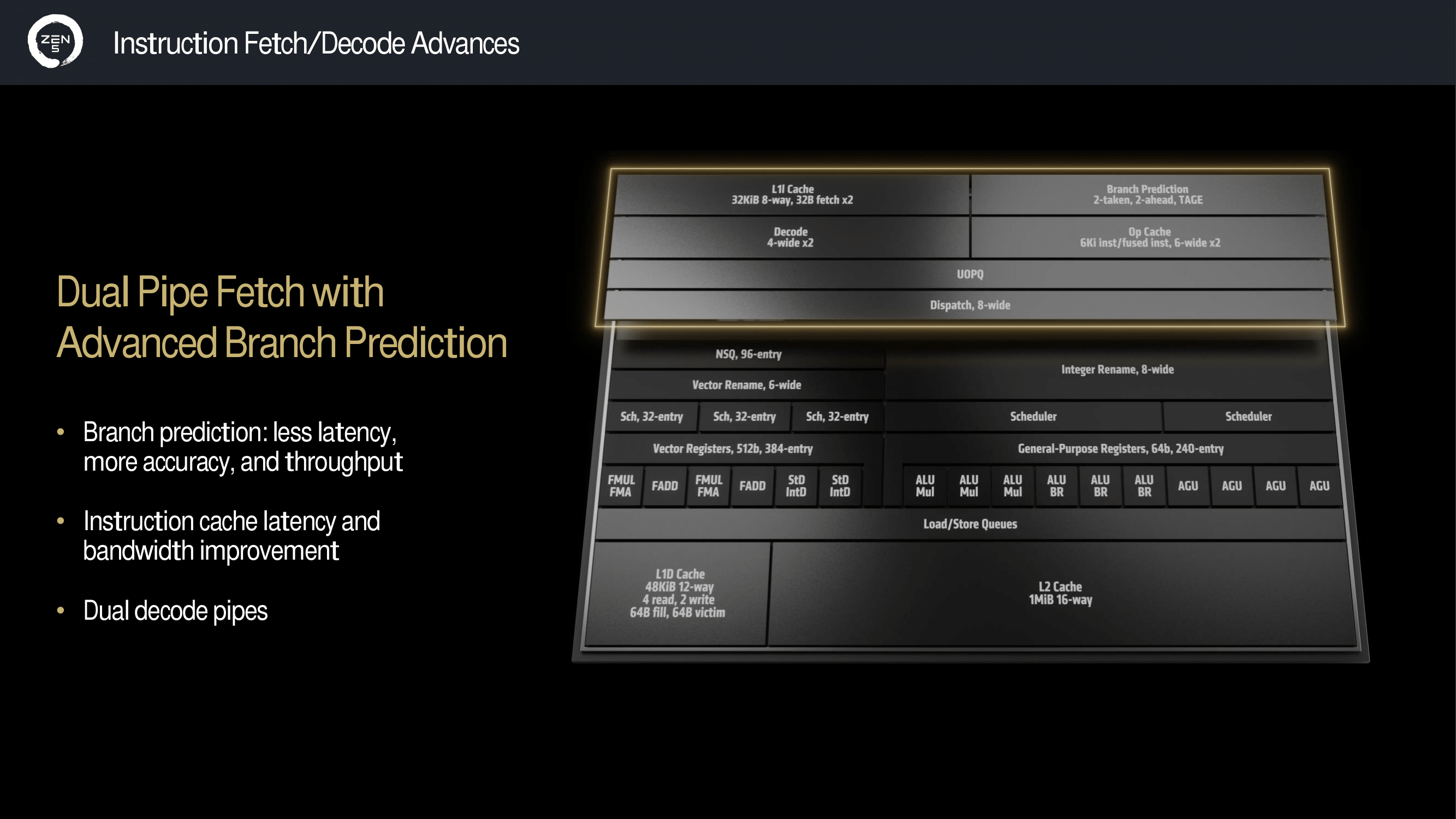
The key features under the hood of the Zen 5 microarchitecture include a dual-pipe fetch, which is coupled with what AMD is calling advanced branch prediction. This is designed to reduce the latency and increase the accuracy and throughput. Enhanced instruction cache latency and bandwidth optimizations further the flow of data and the speed of the data processing without sacrificing accuracy.
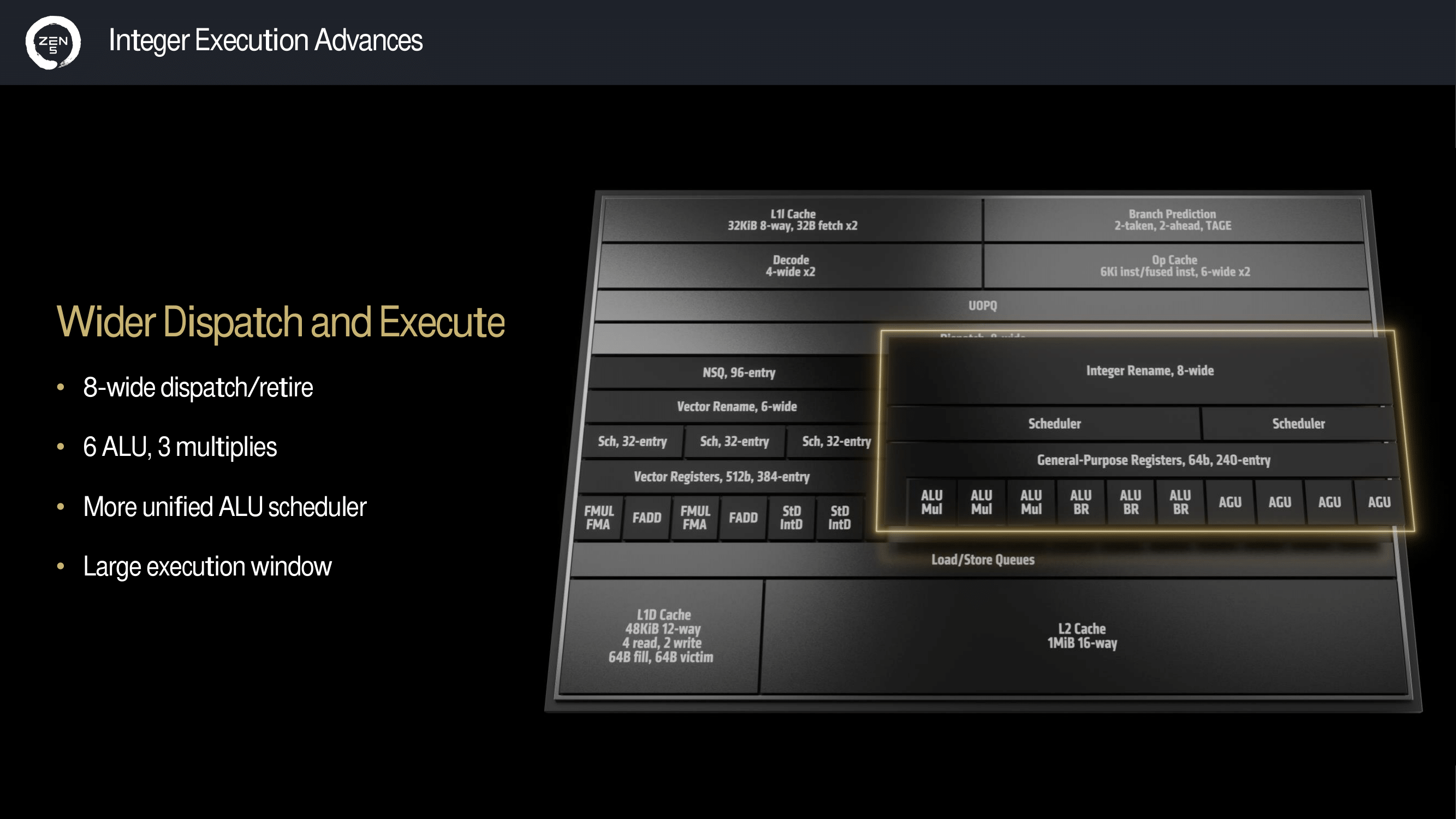
The Zen 5 integer execution capabilities have been upgraded over Zen 4, with Zen 5 featuring an 8-wide dispatch/retire system. Part of the overhaul under the hood for Zen 5 includes six Arithmetic Logic Units (ALUs) and three multipliers, which are controlled through an ALU scheduler, and AMD is claiming Zen 5 uses a larger execution window. These improvements should theoretically be better with more complex computational workloads.
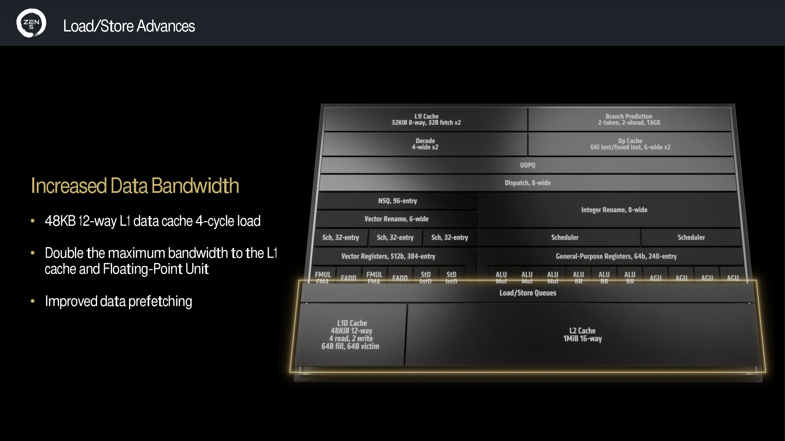
Other key enhancements that Zen 5 comes with include more data bandwidth than Zen 4, with a 48 KB 12-way L1 data cache that can cater to a 4-cycle load. AMD has doubled the maximum bandwidth available to the L1 cache, and the Floating-Point Unit has been doubled over Zen 4. AMD also claims it has improved the data prefetcher, which ensures faster and more reliable data access and processing.
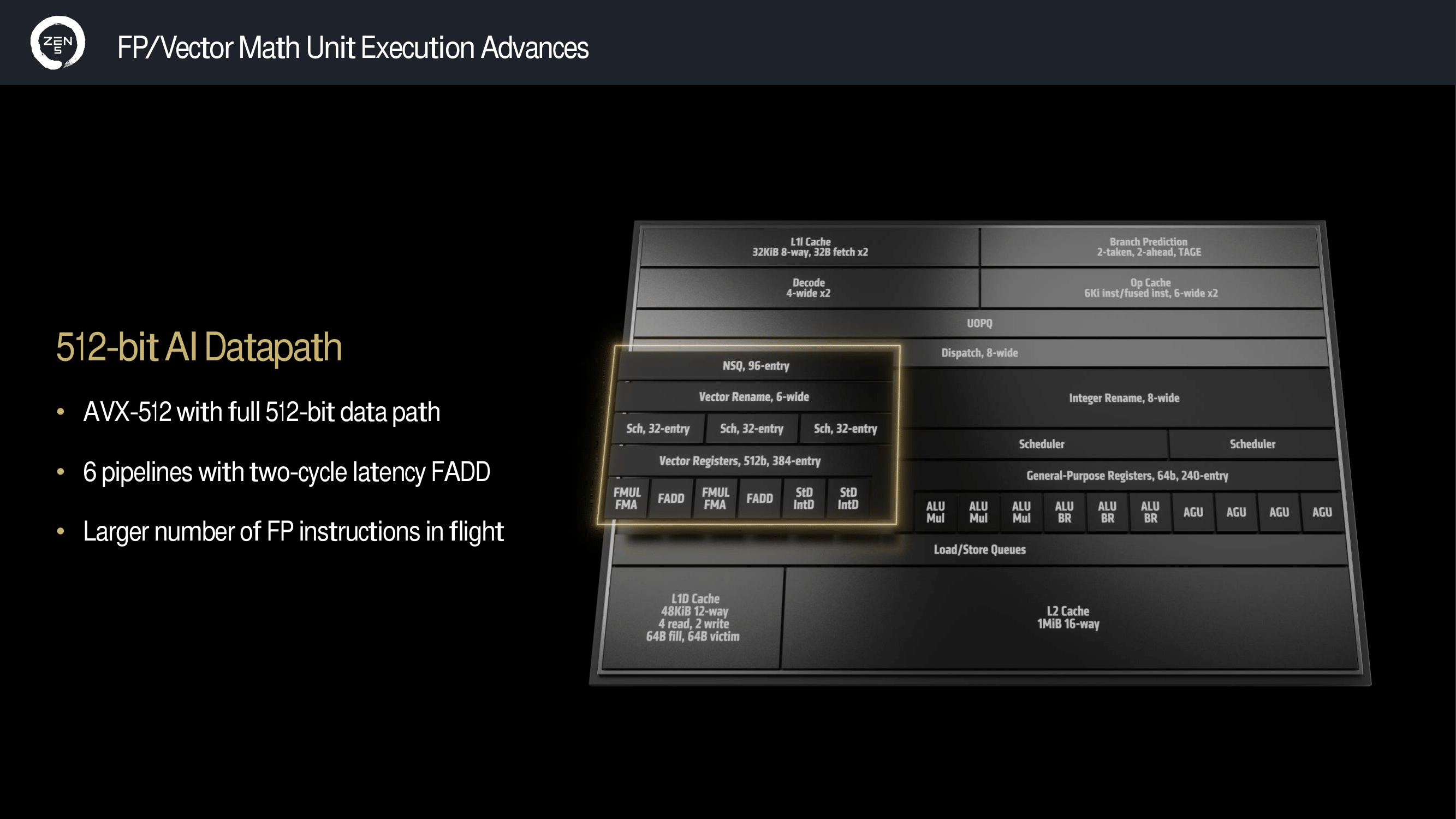
Zen 5 also introduces a full 512-bit AI datapath, which uses AVX-512 with the full 512-bit data path and six pipelines with two-cycle latency FADD. Although Zen 4 can support AVX-512 instructions, it uses two 256-bit data paths that work in tandem with each other, with the term 'double pumping' being the most widely used term for it. Zen 5 now has a full AVX-512 data path, which is a welcomed improvement.
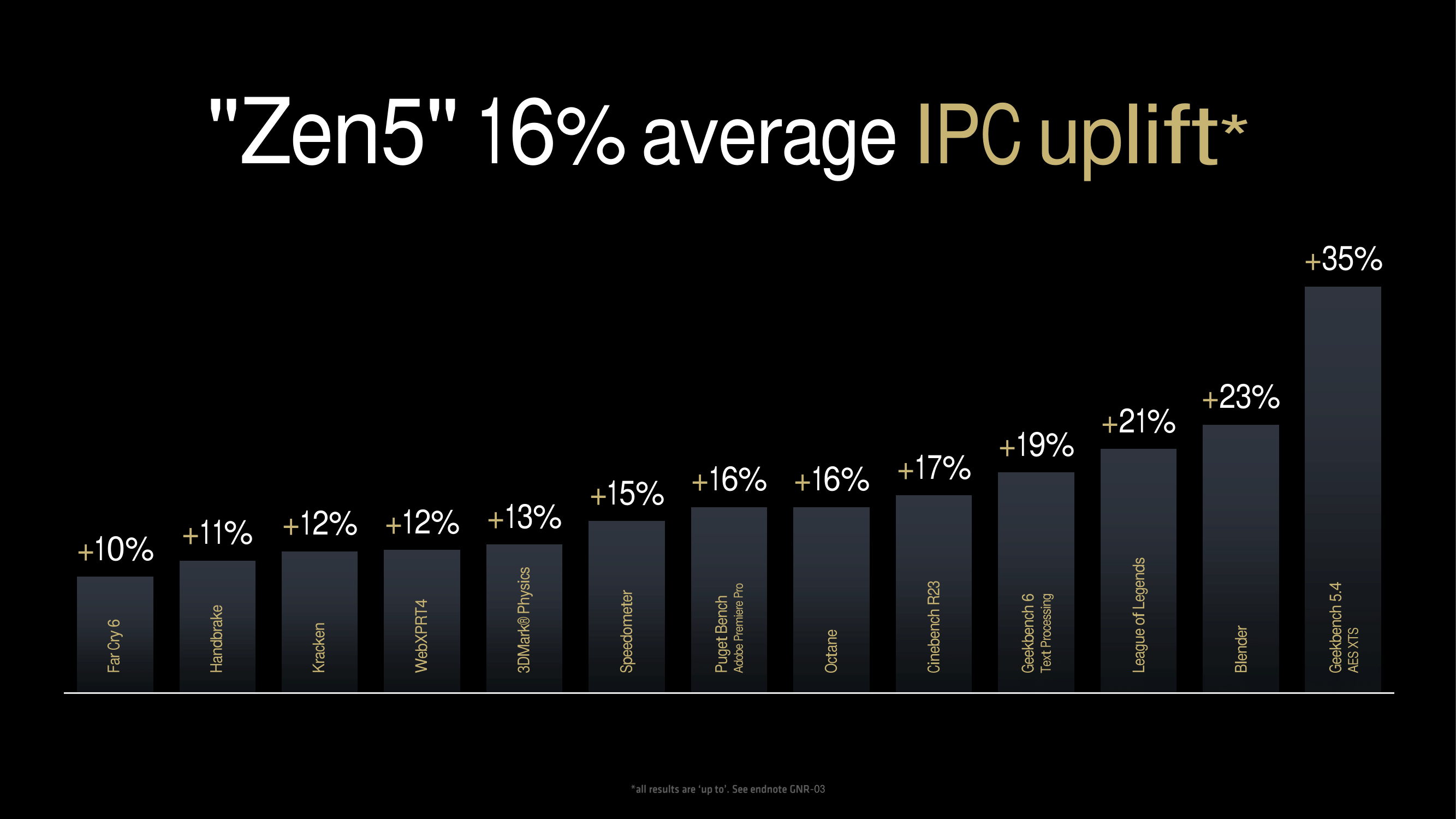
Looking at what AMD is claiming regarding the IPC uplift for Zen 5, AMD claims an average improvement of 16% over Zen 4. AMD has, of course, provided in-house figures, which show across-the-board improvements in various benchmarks. This includes a 10% uptick in Far Cry 6 to 15% in Speedometer and an even bigger uplift of 21% in League of Legends. AMD's biggest claim is a large 35% improvement in Geekbench 5.4 AES-XTS. That's an impressive uplift in performance, although the Geekbench 5 AES XTS test utilizes VAES+ and AVX10/512, which for processors that support these instructions as Zen 5 does can be advantageous.
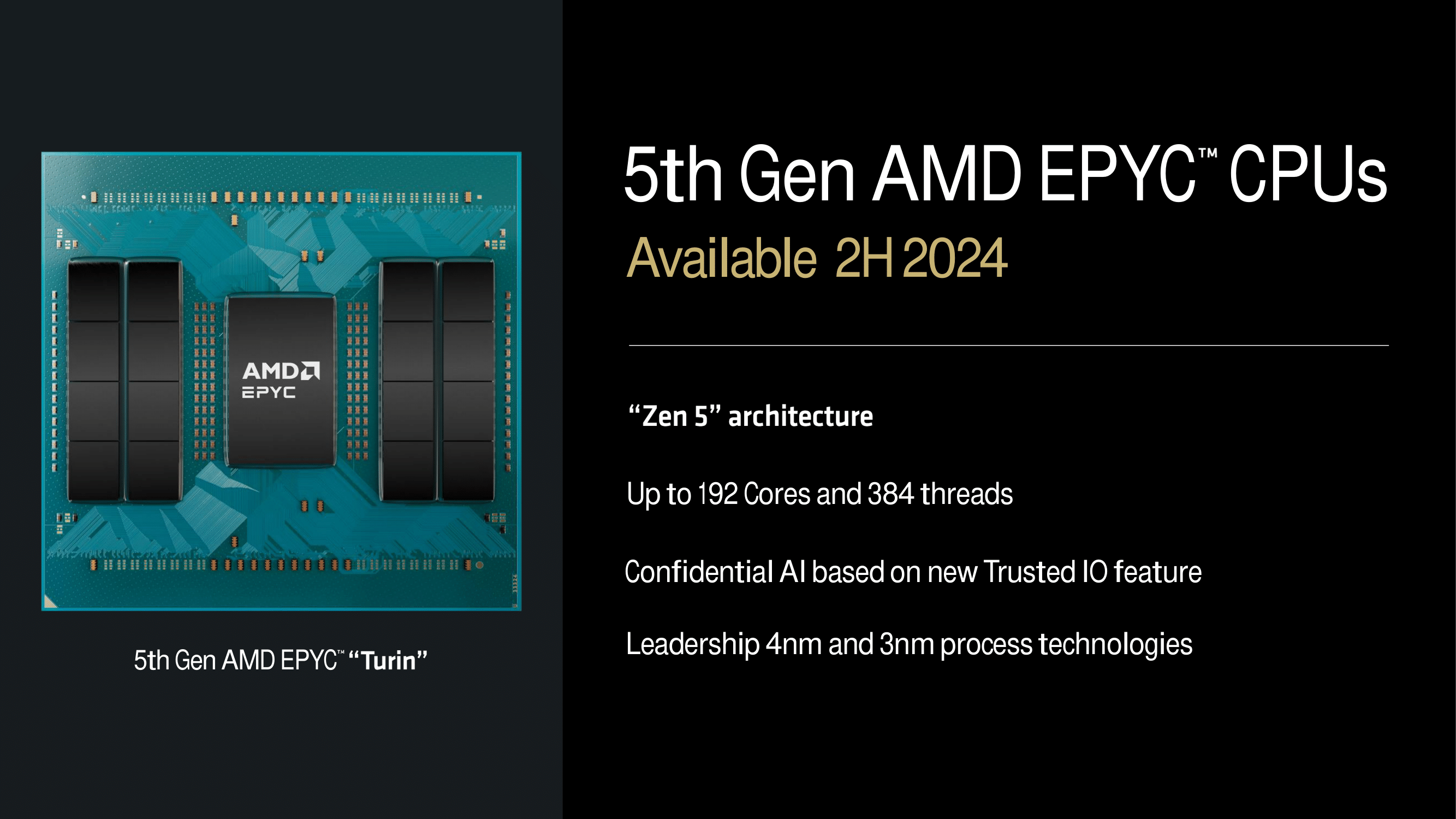
As we've seen through previous iterations of their Zen microarchitecture, AMD is making Zen 5 available across the entire product family. The full-fat Zen 5 cores are made on TSMC's 4nm anode, while the more compact and more power-efficient Zen 5c cores are made on TSMC's 3nm process technology. AMD's upcoming 5th generation EPYC CPUs, codenamed 'Turin,' are expected to launch sometime in the second half of 2024, which leverage up to a whopping 192 Zen 5 cores. AMD previously announced that 5th Gen EPYC would be coming in 2024 back in June 2022 during their Financial Analysts Day.
AMD Ryzen AI 300 Series: A Quick Recap
Leading the pack from AMD's new Ryzen AI 300 series is the Ryzen AI 9 HX 370, with 12 Zen 5 cores up to 5.1 GHz maximum boost frequency and comes with a 24 MB L3 cache. Moving down the stack is the Ryzen AI 9 365, which has 10 Zen 5 cores and can boost up to 5.0 GHz. It has the same 24 MB of L3 cache as the HX 370, just with fewer Zen 5c cores.
| AMD Ryzen AI 300 Series Mobile Processors (Zen 5/Strix Point) |
|||||||
| AnandTech | Cores | Base Freq |
Turbo Freq |
L3 Cache |
Graphics | NPU | TDP |
| Ryzen AI 9 HX 370 | 4x Zen 5 8x Zen5c (24 Threads) |
2.0GHz | 5.1GHz | 24 MB | Radeon 890M 16 CU |
XDNA 2 (50 TOPS) |
15-54W |
| Ryzen AI 9 365 | 4x Zen 5 6x Zen5c (20 Threads) |
2.0GHz | 5.0GHz | 24 MB | Radeon 880M 12 CU |
XDNA 2 (50 TOPS) |
15-54W |
While it's likely AMD will announce more SKUs at a later date, there are just two for now: one from the more performant HX series and one without a prefix. Both Ryzen AI 300 series chips are aimed at high-performance notebooks, and as they have a rather wide TDP range of 15 Watts to 54 Watts, the chips can conceivably be placed in anything from an ultrabook to a desktop replacement laptop.
AMD is using its full-fat Zen 5 cores and incorporating its more compact Zen 5c cores, which should provide some trade-offs in power efficiency vs. performance. While previous models in AMD's Ryzen mobile families had 8 full-fat cores, the Ryzen 300 AI series brings a mixture of regular and compact cores to the table.
The top SKU also wears the HX prefix, which means it's part of the more premium and high performance of AMD's line-up. The Ryzen AI 9 HX 370 is only a 12C/24T part, but with the latest Zen 5 cores backed with AMD's latest Zen 5 microarchitecture under the hood and all of the IPC gains associated with Zen 4, which AMD brings to the table.
Looking at the Ryzen AI 9 365, it is a 10C/20T part with a maximum boost frequency of up to 5.0 GHz, and like the Ryzen AI 9 HX 370, it also comes with the latest RDNA 3.5-based Radeon 890M integrated graphics. Both chips share this particular integrated graphics processing unit (GPU). In our previous article, which announced the AMD Ryzen AI 300 series back at Computex, AMD stated that the AMD RDNA 3.5 Radeon integrated graphics would feature up to 16 graphics compute units, with the Ryzen AI 9 HX 370 coming with 16 compute units, and the Ryzen AI 9 365 with 12 compute units.
AMD Ryzen 9000 Series: Zen 5 For The AM5 Desktop Platform
Quickly recapping AMD's announcement of the Ryzen 9000 series for desktops, which uses the fully-fledged Zen 5 cores built on the TSMC N4 node, four new models are coming at launch, which is officially set for July 31st.
| AMD Ryzen 9000 Series Processors Zen 5 Microarchitecture (Granite Ridge) |
||||||||
| AnandTech | Cores / Threads |
Base Freq |
Turbo Freq |
L2 Cache |
L3 Cache |
Memory Support | TDP | MSRP |
| Ryzen 9 9950X | 16C / 32T | 4.3GHz | 5.7GHz | 16 MB | 64 MB |
DDR5-5600 |
170 W | TBC |
| Ryzen 9 9900X | 12C / 24T | 4.4GHz | 5.6GHz | 12 MB | 64 MB | 120 W | TBC | |
| Ryzen 7 9700X | 8C / 16T | 3.8GHz | 5.5GHz | 8 MB | 32 MB | 65 W | TBC | |
| Ryzen 5 9600X | 6C / 12T | 3.9GHz | 5.4GHz | 6 MB | 32 MB | 65 W | TBC | |
Looking at the specifications of the soon-to-be-launched Ryzen 9000 series, AMD offers four X-series SKUs at launch, which allow for overclocking and come with unlocked CPU multipliers. The flagship SKU, the Ryzen 9 9950X, features 16 cores, a max boost clock of up to 5.7 GHz, 80 MB of cache split between 64 MB for the L3 and 16 MB for the L2 (1 MB per core of L2), and a 170 W TDP. The Ryzen 9 9900X offers 12 cores, a max boost clock of up to 5.6 GHz, 64 MB of L3 cache, and a 120 W TDP.
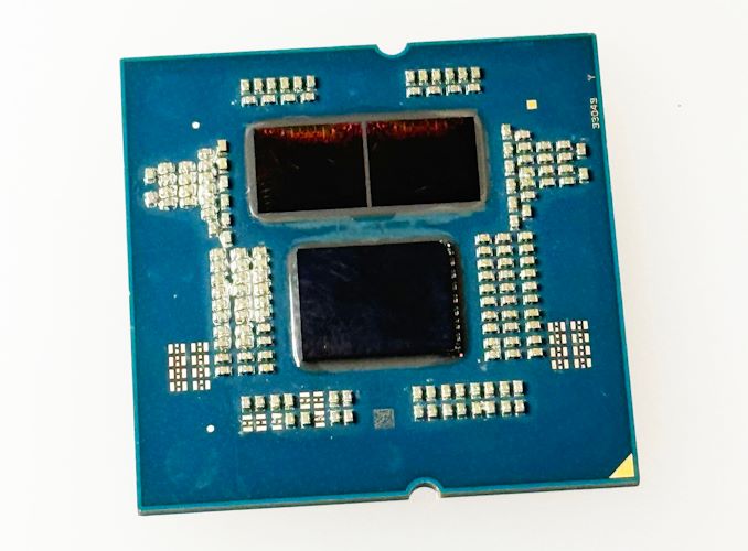
A physical die shot of the AMD Ryzen 9 9950X without the IHS attached
Moving down the Ryzen 9000 stack is the Ryzen 7 9700X, which comes with 8 cores, a max boost clock of up to 5.5 GHz, 32 MB of L3 cache, and a 65W TDP. Finally, the entry-level SKU, the Ryzen 5 9600X, has just 6 cores, a max boost clock of up to 5.4 GHz, 32 MB of L3 cache, and a 65 W TDP.
In terms of design, the Ryzen 9000 with Zen 5 cores and the Ryzen 7000 with Zen 4 cores aren't too dissimilar; after all, they support the same AM5 motherboards with the LGA1718 CPU socket. At Computex 2024, we confirmed that the Ryzen 9000 series actually uses the same I/O die as the Ryzen 7000 series, which was built using TSMC's 6 nm process. The only real difference between the Ryzen 9000 and Ryzen 7000 chips is that the Ryzen 9000 incorporates the latest Zen 5 cores in place of Zen 4 cores.
AMD Ryzen 9000 Overclocking: New Curve Shaper Feature
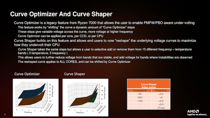
Although the Ryzen 9000 series comes with the Curve Optimizer, which came along with the Zen 3/Ryzen 5000, AMD is introducing a new overclocking feature called Curve Shaper with the Ryzen 9000 and Zen 5 platform.
Looking at AMD's latest overclocking feature specifically designed for Zen 5 and the Ryzen 9000 series, Curve Shaper is essentially an enhanced version of Curve Optimizer, which came with the Ryzen 5000 series. What Curve Shaper is and allows users to do is fine tune voltage curves across 15 different frequency and temperature bands (3 x 5 = 15). This is designed to give users more detailed control over power, CPU VCore, and frequency whilst maintaining stability. Enabling the adjustment of various frequency/voltage bands, which includes three for temperature and five for frequency, allows users to reduce the voltage in stable areas and increase it where necessary. Essentially, AMD's new Curve Shaper feature enables users to push Ryzen 9000 CPUs to their limits while maintaining stability and with an element of power efficiency to boot.
AMD In-House Performance Figures: Ryzen 9000 vs Intel 14th Gen
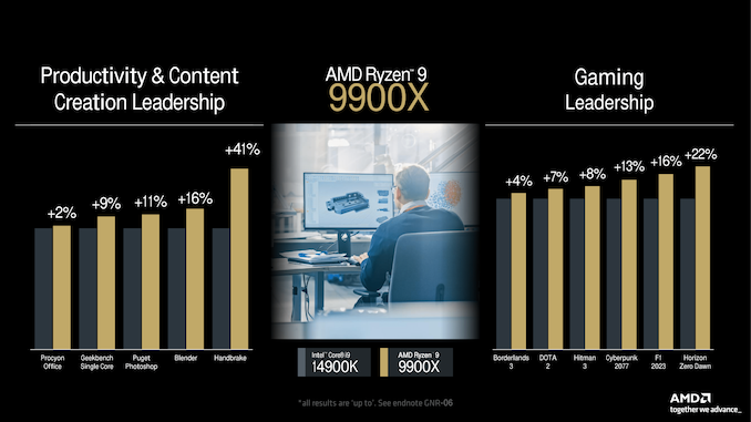
As we always say, take performance figures provided by manufacturers, and that goes for any manufacturer with a pinch of salt. AMD has provided some data through in-house testing, which pits the AMD Ryzen 9 9900X against the Intel Core i9-14900K, the Ryzen 7 9700X vs. the Intel Core i7-14700K, and the Ryzen 5 9600X against the Core i5-14600K.
Starting with the AMD Ryzen 9 9900X (12C/24T vs. the Intel Core i9-14900K (8P+16E/32T), AMD is claiming some pretty impressive performance gains with its Zen 5 cores. While it only has a modest increase of 2% in UL Procyon Office, AMD is boasting a 41% uplift in HandBrake, which is clearly using some form of AVX-512 workload, as it's a massive jump over the 2% to the 22% gains in other areas such as in Horizon Zero Dawn, while AMD is claiming the Ryzen 9900X is 16% better in Blender. It also shows the strength of AMD's Zen 5 cores in terms of performance, although that remains to be seen when reviews come out. It still looks very promising, though.
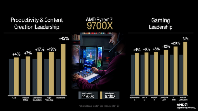
Moving to the Ryzen 7 9700X (8C/16T) vs. the Core i7-14700K (8P+12E/28T), AMD is claiming victories across a plethora of benchmarks, including 7-Zip, UL Procyon Office, and HandBrake (technically, Intel 14th Gen doesn't officially support AVX-512), which is where the 42% gain in performance is obviously coming from. In gaming, AMD is claiming between 4% and 31% gains in titles, which vary between Borderlands 3 (4%) and Horizon Zero Dawn, which is at the top end with 31%. Given the Ryzen 7 9700X has fewer cores, again, it shows how fast and high-performance AMD's latest Zen 5 cores are.
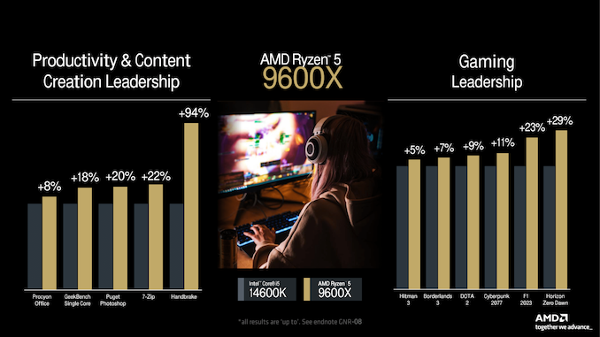
Lastly, we have the Ryzen 5 9600X (6C/12T) vs. the Core i5-14600K (6P+8E/;20T), and we see a similar uplift in the same benchmarks as used in the other comparisons. Again, HandBrake's performance is through the roof at 94%, which clearly uses AVX-512 or some variant within the workload itself. Still, AMD is claiming between 8% and 22% in the other compute benchmarks and uplifts of between 5% and 29% in games, including Hitman 3, Borderlands 3, and F1 2023.
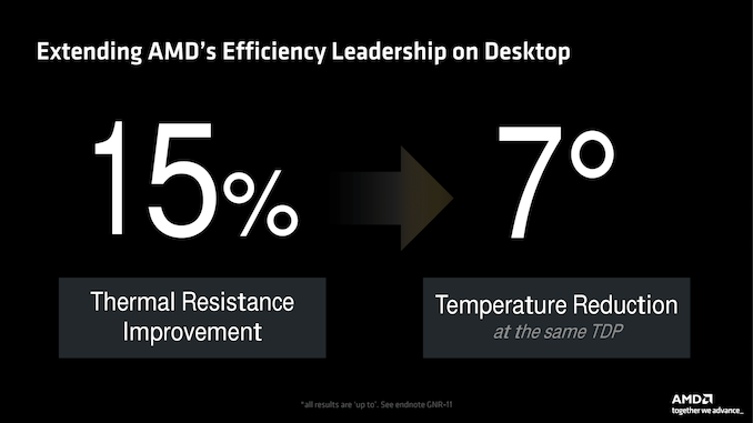
Something else AMD is claiming is that they have improved the overall thermal resistance of the CPUs and managed to reduce the operating temperatures with the Ryzen 9000 processors (Zen 5) over the previous Ryzen 7000 (Zen 4) series. In terms of thermal resistance, AMD claims a 15% improvement over Ryzen 7000. At the same time, they also claim they have managed to reduce operating temperatures by 7°C when operating at a like-for-like TDP. Unfortunately, when asked at the Tech Day in LA last week, AMD wouldn't divulge how they managed these improvements, but that's not a surprise.
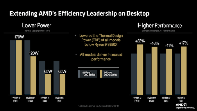
Outside of the flagship Ryzen 9 9950X, AMD has actually lowered the TDP on all the models below it when compared to the previous generation. Meanwhile, the Ryzen 9 7900X has a TDP of 170 W, and the correlating replacement, the Ryzen 9 9900X, has a TDP of just 120 W. This goes for the Ryzen 7 and Ryzen 5 series, too, which has dropped down to a very power-efficient 65 W TDP.
Despite operating with a lower TDP, comparing performance like-for-like, the Zen 5 cores perform up to 22% higher on the Ryzen 9 9950X vs. the Ryzen 9 7950X, while even the Ryzen 9 9900X with a 120 W TDP against the previous Ryzen 9 7900X (170 W), performs up to 16% higher. One thing AMD's Zen microarchitecture is known for is its power efficiency, as well as how much performance is retained when operating at a lower wattage than TDP. We did some power scaling testing with the Ryzen 9 7950X against the Intel Core i9-13900K, and we were impressed with how much performance the Zen 4 cores managed to retain despite operating at much lower than stock in relation to TDP.
As we've known since the AM5 platform launched alongside the Ryzen 7000 series chips back in 2022, AMD's Zen 5 chips would be supported on the current AM5 chipset available, including X670E, X670, B650E, and B650 motherboards. While there is a new wave of AM5 motherboards coming (when is a question rather than an answer for now), which are denoted as the 800-series (X870E/X870/B850/B840), with some motherboard vendors showing models off back at Computex 2024 in June. There's been some speculation about when these will launch; as for now, there is no official date for these 800-series motherboards to launch. This means users looking to buy a Ryzen 9000 series processor at launch will either have to use their current AM5 motherboard or buy a 600-series board.
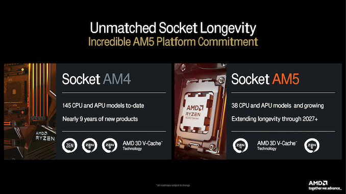
In reality, both the 600-series and 800-series AM5 motherboards use the same Promotory 21 chipset (PROM21), which is made by ASMedia. The only real difference between the chipsets is that motherboard vendors can use the latest controllers, such as Wi-Fi 7. Otherwise, there shouldn't be any gains in performance when opting for an 800-series board instead of a 600-series motherboard. AMD has, however, committed that the AM5 platform will be one of longevity, with the AM5 platform being the desktop platform for desktop Ryzen CPUs until 2027.
Over the next couple of pages, we will be going over some of the technical details AMD disclosed during its Tech Day 2024 in LA, which is primarily around the AMD Ryzen AI 300 series SoCs. This includes the new AMD Xilinix-built XDNA 2 NPU for AI, as well as AMD's updated RDNA 3.5-based integrated graphics.
AMD Ryzen AI 300: XDNA 2 NPU with Up To 50 TOPS
When it comes to the AMD Ryzen AI 300 series for notebooks and laptops, the second biggest advancement from the previous Ryzen 8040 series (Hawk Point) is through the Neural Processing Unit (NPU). AMD, through their acquisition of Xilinx back in 2020, jump-started their NPU development by integrating Xilinx's existing technology, leading to AMD's initial XDNA architecture. With their latest iteration of the architecture, XDNA 2, AMD is further expanding on its capabilities as well as its performance. It also introduces support for the Block Floating Point 16-bit arithmetic approach as opposed to the traditional half-precision (FP16), which AMD claims to combine the performance of 8-bit but with the accuracy of 16-bit.
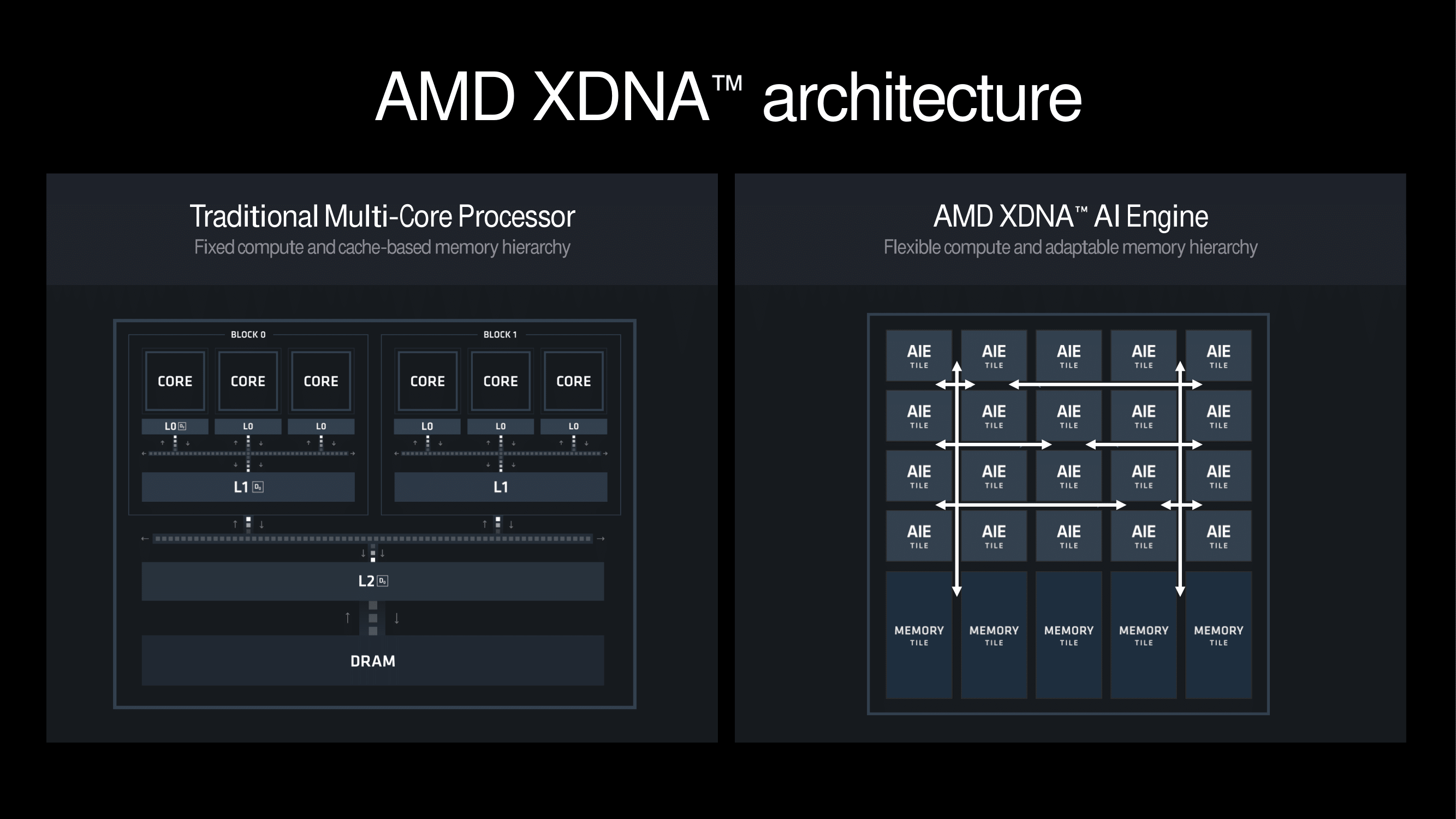
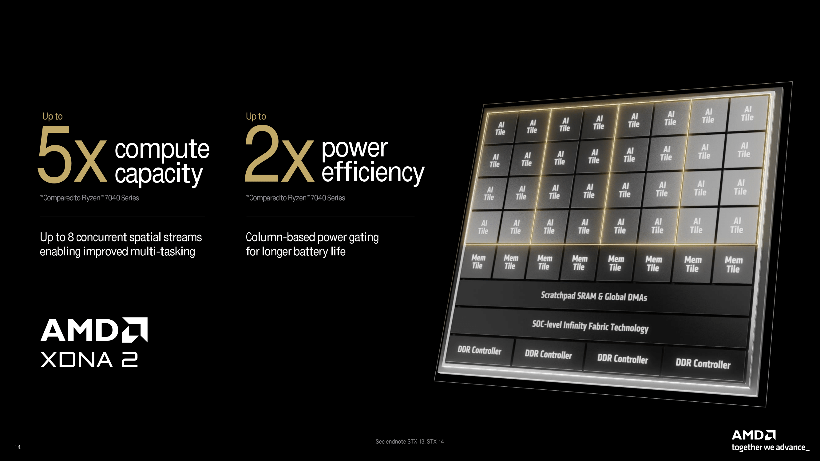
Looking at how the AMD XDNA architecture differs from the typical design of a multicore processor, the XDNA design must incorporate a flexible compute with an adaptive memory hierarchy. Compared to models of fixed compute or a model based on a static memory hierarchy, the XDNA (Ryzen AI) Engine uses a grid of interconnected AI Engines (AIE). Each engine has been architected to be able to dynamically adapt to the task at hand, including computation and memory resources, which are designed to improve scalability and efficiency.
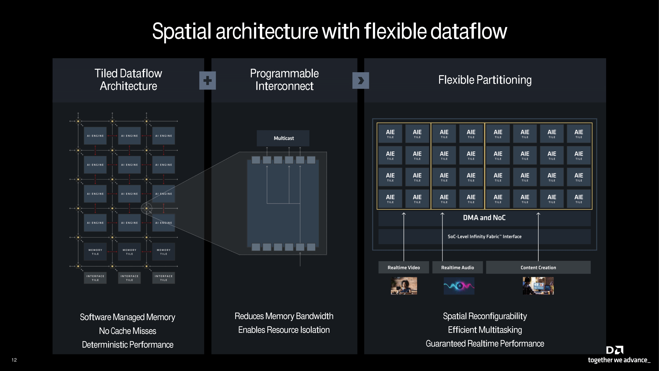
Touching more on the tiled approach to the AIE, AMD calls this spatial architecture. It is designed to be flexible, while it couples a tiled dataflow structure with programmable interconnection and flexible partitioning. The tiled dataflow structure enables deterministic performance without any cache misses and also enhances memory management. A programmable interconnect substantially decreases the demand for memory bandwidth, which allows it to allocate resources efficiently. The flexible partitioning design used enables real-time performance while being able to accommodate different requirements, from a variety of AI inferencing tasks, including real-time video and audio processing, to content-creation workflows.
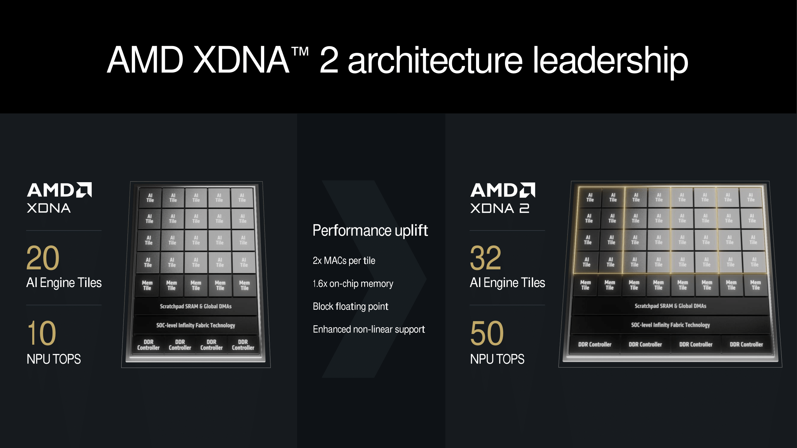
The XDNA 2 architecture builds upon the preexisting XDNA architecture and adds even more AI engines to increase throughput. The AMD XDNA 2 implementation in Strix Point has 32 AI engine tiles, which is 12 more than the previous generation. Not only giving more AI engine tiles, the XDNA 2 architecture also has double the number of MACs per tile and 1.6 X more on-chip memory than the previous generation.
All told, AMD is claiming 50 TOPS of NPU performance, which is more than Intel and Qualcomm's current offerings. The debate around the relevancy of using TOPS to measure AI performance is divisive, and Microsoft set the ball rolling on that one by setting the bar for Copilot+ at 40 TOPS.
Not just about trying to outdo the competition on TOPS, but the XDNA 2 architecture is also designed with power efficiency in mind. AMD claims that its XDNA 2 NPU provides 5x the compute capacity at double the power efficiency compared to the NPU used in the Ryzen 7040 Series. This is made possible through various design choices, including the column-based power gating that AMD says it offers significantly better battery life with the ability to simultaneously handle as many as eight concurrent spatial streams when multitasking.
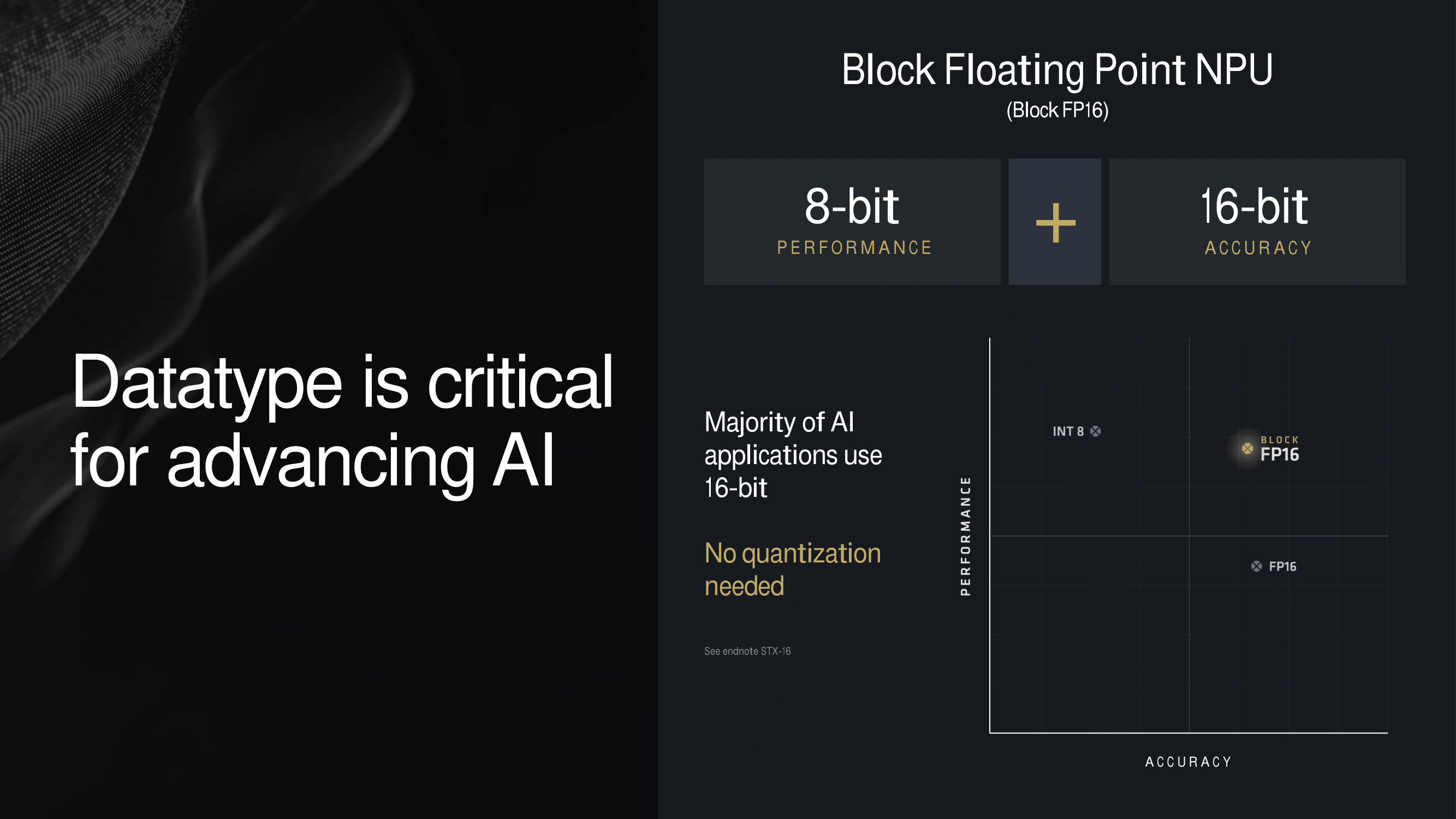
One of the major feature inclusions with the XDNA 2 architecture is support for the Block Floating Point (Block FP16). The simple way to explain what it does is it offers the performance and speed of 8-bit operations, but employs additional tricks to try to bring the precision closer to 16-bit operations. Notably, this is also done without further quantization or reducing the data size being processed.
As with other neural network precision optimizations, the purpose of Block FP16 is to cut down on the amount of computational work required; in this case using 8-bit math without incuring the full drawbacks of stepping down from 16-bit math – namely, poorer results from the reduced precision. Current generation NPUs can already do native 8-bit processing (and 16-bit, for that matter), but this requires developers to either optimize (and quantize) their software for 8-bit processing, or take the speed hit of staying at 16-bit. AI is still a relativley young field, so software developers are sitll working to figure out just how much precision is enough (with that line seeming to repeatedly drop like a limbo bar), but the basic idea is that this tries to let software developers have their cake and eat it, too.
With all of that said, from a technical perspective, Block FP16 (aka Microscaling) is not a new technique in and of itself. But AMD will be the first PC NPU vender to support it, with Intel's forthcoming Lunar Lake set to join them. So while this is a new-to-AMD feature, it's not going to be a unique feature.
As for how Block FP16 works, AMD's own material on the subject is relatively high-level, but we know from other sources that it's essentially a form of fixed point 8-bit computation with an additional exponent. Specifically, Block FP16 uses a shared exponent for all values, rather than each floating point value having its own exponent. For example, rather than a FP16 number having a sign bit, 5-bit exponent, and 10-bit significant, you have an 8-bit exponent that's shared with all numbers, and then an 8-bit significand.
This essentially allows the processor to cheat by processing the unique significands as INT8 (or fixed-point 8-bit) numbers, while skipping all the work on the shared exponent. Which is why Block FP16 performance largely matches INT8 performance: it's fundamentally 8-bit math. But by having a shared exponent, software authors can move the whole number range window for the computation to a specific range, one that would normally be outside of the range offered by the puny exponent of a true FP8 number.
Most AI applications require 16-bit precision, and Block FP16 addresses this requirement by simultaneously bringing high performance and high accuracy to the mobile market, at least from an AI standpoint. This makes Block FP16 a very important component for pushing forward AI technology, and it is something AMD is pushing hard on.
Ultimately, the XDNA 2-based NPU in the Ryzen AI 300 series of mobile chips is really about processing AI workloads and running features such as Microsoft Copilot+ in a more power-efficient manner than using the graphics. And by being able to deliver 8-bit performance and 16-bit precision, that gives developers one more lever to pull to get the most out of the hardware.
The AMD XDNA 2 architecture, which is set to debut with the Ryzen AI 300 series, is going to provide the key to unlocking the AI PC, or at least what Microsoft defines with their 40 TOPS requirement for Copilot+. By bringing Block FP16 into the equation, AMD brings (close to) 16-bit accuracy at 8-bit speed, making it more performant for some AI applications. Altogether, the integrated NPU is slated to offer up to 50 TOPS of compute performance.
AMD was the first x86 SoC vendor to include an NPU within their chips, and with the growing need for on-chip AI solutions to unlock many software features, they're expecting the hardware (and the die space it represents) to be put to good use. The XDNA 2 architecture ensures that AMD remains at the forefront, offering solid levels of performance and combined versatility for the mobile market.
AMD Ryzen AI 300: RDNA 3.5 Graphics Brings The Visuals
Another new technology coming with Zen 5 for the Ryzen AI 300 mobile series chips is upgraded integrated graphics. AMD's RDNA 3.5 graphics architecture represents what looks to be a stepping stone (sans the .5) to the next generation of AMD's graphics architecture. This latest iteration has been designed to enhance both performance and efficiency, with a focus on optimizing every last drop of performance per watt. It's worth noting that AMD hasn't provided many details about RDNA 3.5, so we'll dive into the key features and advancements.
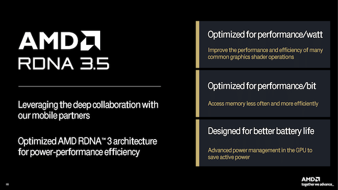
The AMD RDNA 3.5 graphics architecture represents the next step in integrated graphics for their Ryzen AI 300 mobile SoCs, with some notable upgrades over RDNA 3. AMD has been working closely with ISVs and developers to ensure that RDNA 3.5 provides everything AMD says it will be working hand-in-hand with mobile partners for better performance per watt in games. Some improvements include general graphic shader operations, which are optimized to ensure things work as they should. AMD has put a lot of focus on the performance per bit, which not only reduces the times of memory accesses but it also makes the operations smoother. The general cusp of the improvements is all around power vs. performance, with AMD aiming for the middle ground to ensure a longer battery life, which is vital in mobile and portable devices.
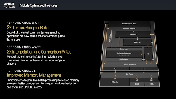
Much of the improvements over RDNA 3 come through several features that have been specially optimized for mobile platforms. This ensures that the Radeon 890M, which is the model with the Ryzen AI 300 series, has the best of both worlds in terms of efficiency and visual performance. The rate of texture sampling has been doubled, which ensures double-rate performance from the GPU. What it means on the surface is enhanced detail and clarity of the textures and graphics during gameplay. This, in theory, should help improve detailed textures so they look great when playing high-resolution games. Further to this, RDNA 3.5 has 2X the interpolation and comparison rate, as vector ISA operations can work much better to bring out detail in high-quality graphics.
Another critical improvement is better memory management techniques. These reduce the frequency of memory access, meaning data processing should, in theory, be faster and overall more energy-efficient. Optimized LPDDR5 access should also guarantee fast and efficient memory use, which in turn should aid battery life.
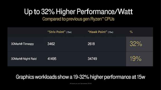
AMD has provided some performance figures comparing RDNA 3.5 to RDNA 3, with some pretty impressive claims if they translate into real-world performance. On paper, the RDNA 3.5 architecture shows a significant performance uplift compared to the previous generation Ryzen 8040 series, with up to 32% higher performance per watt. In graphics workloads like 3DMark Timespy and 3DMark Night Raid, AMD claims that RDNA 3.5 has an uplift of between 19 and 32% in terms of performance at 15 W.
Because of these improvements, RDNA 3.5 is improved in various ways compared to its predecessor, RDNA 3. For example, RDNA 3.5 greatly increases the GPU's capacity to execute complicated graphics operations more effectively by optimizing key things such as texture sampling and interpolation. Improving the memory management in RDNA 3.5 also allows for better power optimization and data handling to address major GPU performance issues. All of these should bring real-world performance benefits. However, as with any mobile SoC, these still aren't on the level of discrete graphics, which typically have more die area to play with, a higher transistor budget at the manufacturing level, and, of course, more power.

