Original Link: https://www.anandtech.com/show/18963/samsung-completes-initial-gddr7-development-first-parts-to-reach-up-to-32gbpspin
Samsung Completes Initial GDDR7 Development: First Parts to Reach Up to 32Gbps/pin
by Ryan Smith on July 18, 2023 11:00 PM EST
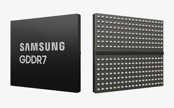
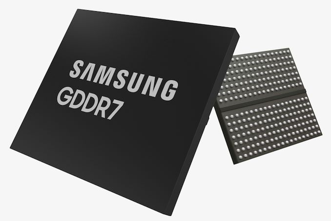
Samsung has announced this evening that they have completed development on their first generation of GDDR7 memory. The next iteration of the high bandwidth memory technology, which has been under industry-wide development, is expected to hit the market in 2024, with Samsung in prime position to be one of the first memory vendors out of the gate. With their first generation of GDDR7 parts slated to hit up to 32Gbps/pin of bandwidth – 33% more than their best GDDR6 parts today – the company is looking to deliver a sizable increase in GDDR memory bandwidth on the back of the technology’s adoption of PAM-3 signaling.
Samsung’s announcement comes as we’ve been seeing an increase in disclosures and announcements around the next iteration of the widely-used memory technology. While a finished specification for the memory has yet to be released by JEDEC, Samsung rival Micron has previously announced that it plans to introduce its own GDDR7 memory in 2024 – a similar timeline as to Samsung’s current schedule. Meanwhile, EDA tool firm Cadence disclosed a significant amount of technical details earlier this year as part of announcing their GDDR7 verification tools, revealing that the memory would use PAM-3 signaling and reach data rates of up to 36Gbps/pin.
With today’s announcement, Samsung has become the first of the major memory manufacturers to publicly announce that they’ve completed development of their first generation of GDDR7. And while the company tends to make these sorts of memory announcements relatively early in the bring-up process – well before memory is ready for commercial mass product – it’s none the less an important milestone in the development of GDDR7, as it means that memory and device manufacturers can begin validation work against functional hardware. As for Samsung itself, the announcement gives the Korean conglomerate a very visible opportunity to reinforce their claim of leadership within the GDDR memory industry.
Besides offering an update on the development process for GDDR7, Samsung’s announcement also provides some high-level technical details about the company’s first generation of GDDR7 – though “high-level” is the operative word as this is not by any means a technical deep dive.
| GPU Memory Math | |||||
| GDDR7 | GDDR6X | GDDR6 | |||
| B/W Per Pin | 32 Gbps (Projected) | 24 Gbps (Shipping) | 24 Gbps (Sampling) | ||
| Chip Density | 2 GB (16 Gb) | 2 GB (16 Gb) | 2 GB (16 Gb) | ||
| Total B/W (256-bit bus) | 1024 GB/sec | 768 GB/ssec | 768 GB/ssec | ||
| DRAM Voltage | 1.2 V | 1.35 V | 1.35 V | ||
| Data Rate | QDR | QDR | QDR | ||
| Signaling | PAM-3 | PAM-4 | NRZ (Binary) | ||
| Packaging | 266 FBGA | 180 FBGA | 180 FBGA | ||
According to Samsung’s announcement, they’re expecting to reach data rates as high as 32Gbps/pin. That’s 33% higher than the 24Gbps data rate the company’s top GDDR6 products can hit today. Samsung and Cadence have both previously disclosed that they expect GDDR7 memory to eventually hit 36Gbps/pin, though as with the development of GDDR6 – a full 50% faster than GDDR6 – this is likely going to take multiple generations of products.
Interestingly, this is starting much closer to projected limits of GDDR7 than we’ve seen in past generations of the memory technology. Whereas GDDR6 launched at 14Gbps and eventually scaled up to 24Gbps, Samsung wants to start at 32Gbps. At the same time, however, GDDR7 is going to be a smaller generational leap than we saw for GDDR6 or GDDR5; rather than doubling the signaling bandwidth of the memory technology over its predecessor, GDDR7 is only a 50% increase, owing to the switch from NRZ (2 state) signaling to PAM-3 (3 state) signaling.
It’s also worth noting that, at present, the fastest GDDR6 memory we see used video cards is only running at 20Gbps.Samsung’s own 24Gbps GDDR6, though announced just over a year ago, is still only “sampling” at this time. So the multitude of other GDDR6-using products notwithstanding, the effective jump in bandwidth for video cards in 2024/2025 could be more significant, depending on just what speed grades are available at the time.
As for capacity, Samsung’s first GDDR7 chips are 16Gb, matching the existing density of today’s top GDDR6(X) chips. So memory capacities on final products will not be significantly different from today’s products, assuming identical memory bus widths. DRAM density growth as a whole has been slowing over the years due to scaling issues, and GDDR7 will not be immune to that.
Samsung is also claiming that their GDDR7 technology offers a “20%-improvement in power efficiency versus existing 24Gbps GDDR6 DRAM,” though this is a broad claim where the devil is in the details. As power efficiency for DRAM is normally measured on a per-bit basis (picojoules-per-bit/pJpb), then our interpretation is that this is the figure Samsung is referencing in that claim.
Update (7/19, 3pm ET): Following a round of Q&A, Samsung has provided some additional technical details on their first-generation GDDR7 memory, including voltages (1.2v), how they are measuring energy efficiency, and the process node being used (D1z). The rest of the article has been updated accordingly.
At a high level, the good news is that Samsung’s GDDR7 is slated to deliver a tangible increase in energy efficiency. With a nominal voltage of 1.2v, GDDR7 requires less voltage to drive it than its predecessor. But with only a 20% overall improvement in energy efficiency for a memory technology that is delivering up to 33% more bandwidth, this means that the absolute power consumption of the memory is going up versus the previous generation. As Samsung’s energy efficiency figures are for GDDR7@32Gbps versus GDDR6@24Gbps, we're looking at around a 7% increase in total energy consumption. Which, thankfully, is not a huge increase in power consumption. But it is an increase none the less.
Broadly speaking, this is the same outcome as we saw with the introduction of GDDR6(X), where despite the energy efficiency gains there, overall power consumption increased from one generation to the next, as energy efficiency gains are not keeping pace with bandwidth demands. Not to say that any of this is unexpected, but it means that good cooling will be even more critical for GDDR7 memory.
But for clients with strict power/cooling needs, Samsung is also announcing that they will be making a low-voltage version of their GDDR7 memory available. This will be a 1.1v version of their GDDR7 chips, and while clockspeeds haven't been disclosed, we'd expect something closer to their GDDR6 clockspeeds. With current-generation GDDR6, high-end laptops are typically paired with low-voltage memory running no faster than 18Gbps, so low-voltage GDDR7 running at around 24Gbps would still represent a significant step forward.
Samsung has also confirmed that they're going to be using their D1z memory fab process for their first generation GDDR7. This is the same EUV-based process the company is using for their most recent GDDR6 – but curiously, it's older than the 12nm process Samsung revealed they'll be using elsewhere in a recent DDR5 memory announcement. The fact that the company isn't using a newer node here is a bit surprising, but from an architectural perspective, it also means that Samsung has achieved a 20% increase in energy efficiency without a newer node. Architecturally-driven energy gains are few and far between in both the memory and logic spaces these days, all of which makes for a promising sign for the future of GDDR7.
Speaking of architecture and design, the company notes that their GDDR7 memory employs “IC architecture optimization” to keep power and heat generation in check. Though at this point we don't have any further details on just what that means.
Electronics production aside, the final major innovation with Samsung’s GDDR7 will be decidedly physical: epoxy. Clearly mindful of the already high heat loads generated by existing GDDR memory clocked at its highest speeds, Samsung’s press release notes that they’re using a new epoxy molding compound (EMC) for GDDR7, which is designed to better transfer heat. All told, Samsung is claiming a 70% reduction in thermal resistance versus their GDDR6 memory, which should help ensure that a good cooler can still pull enough heat from the memory chips, despite the overall increase in heat generation.
Wrapping things up, now that initial development on their GDDR7 memory has been completed, Samsung is moving on to verification testing with their partners. According to the company, they’ll be working with key customers on verification this year; though at this point, the company isn’t saying when they expect to kick off mass production of the new memory.
Given the timing of Samsung’s announcement (as well as Micron’s), the initial market for GDDR7 seems to be AI and networking accelerators, rather than the video cards that GDDR7 gets its name from. With both AMD and NVIDIA barely a quarter of the way through their current architectural release cycles, neither company is likely be in a position to use GDDR7 in 2024 when it’s ready. Instead, it’s going to be the other users of GDDR memory such as networking products and high-performance accelerators that are likely to be first to use the technology.
Source: Samsung


