Original Link: https://www.anandtech.com/show/18915/amd-expands-mi300-family-with-mi300x-gpu-only-192gb-memory
AMD Expands AI/HPC Product Lineup With Flagship GPU-only Instinct MI300X with 192GB Memory
by Ryan Smith on June 13, 2023 2:32 PM EST
Alongside their EPYC server CPU updates, as part of today’s AMD Data Center event, the company is also offering an update on the status of their nearly-finished AMD Instinct MI300 accelerator family. The company’s next-generation HPC-class processors, which use both Zen 4 CPU cores and CDNA 3 GPU cores on a single package, have now become a multi-SKU family of XPUs.
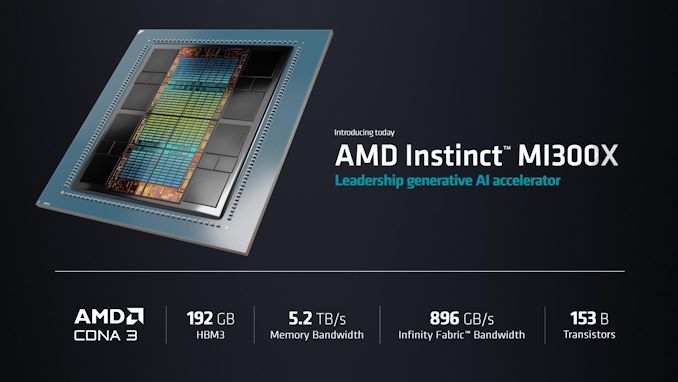
Joining the previously announced 128GB MI300 APU, which is now being called the MI300A, AMD is also producing a pure GPU part using the same design. This chip, dubbed the MI300X, uses just CDNA 3 GPU tiles rather than a mix of CPU and GPU tiles in the MI300A, making it a pure, high-performance GPU that gets paired with 192GB of HBM3 memory. Aimed squarely at the large language model market, the MI300X is designed for customers who need all the memory capacity they can get to run the largest of models.
First announced back in June of last year, and detailed in greater depth back at CES 2023, the AMD Instinct MI300 is AMD’s big play into the AI and HPC market. The unique, server-grade APU packs both Zen 4 CPU cores and CDNA 3 GPU cores on to a single, chiplet-based chip. None of AMD’s competitors have (or will have) a combined CPU+GPU product like the MI300 series this year, so it gives AMD an interesting solution with a truly united memory architecture, and plenty of bandwidth between the CPU and GPU tiles.
MI300 also includes on-chip memory via HBM3, using 8 stacks of the stuff. At the time of the CES reveal, the highest capacity HBM3 stacks were 16GB, yielding a chip design with a maximum local memory pool of 128GB. However, thanks to the recent introduction of 24GB HBM3 stacks, AMD is now going to be able to offer a version of the MI300 with 50% more memory – or 192GB. Which, along with the additional GPU chiplets found on the MI300X, are intended to make it a powerhouse for processing the largest and most complex of LLMs.
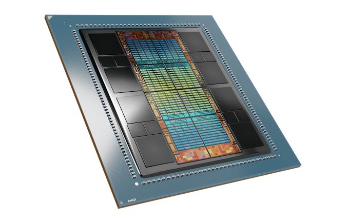
Under the hood, MI300X is actually a slightly simpler chip than MI300A. AMD has replaced MI300A's trio of CPU chiplets with just two CDNA 3 GPU chiplets, resulting in a 12 chiplet design overall - 8 GPU chiplets and what appears to be another 4 IO memory chiplets. Otherwise, despite excising the CPU cores (and de-APUing the APU), the GPU-only MI300X looks a lot like the MI300A. And clearly, AMD is aiming to take advantage of the synergy in offering both an APU and a flagship CPU in the same package.
Raw GPU performance aside (we don't have any hard numbers to speak of right now), a big part of AMD's story with the MI300X is going to be memory capacity. Just offering a 192GB chip on its own is a big deal, given that memory capacity is the constraining factor for the current generation of large language models (LLMs) for AI. As we’ve seen with recent developments from NVIDIA and others, AI customers are snapping up GPUs and other accelerators as quickly as they can get them, all the while demanding more memory to run even larger models. So being able to offer a massive, 192GB GPU that uses 8 channels of HBM3 memory is going to be a sizable advantage for AMD in the current market – at least, once MI300X starts shipping.
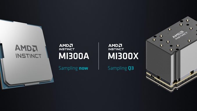
The MI300 family remains on track to ship at some point later this year. According to AMD, the 128GB MI300A APU is already sampling to customers now. Meanwhile the 192GB MI300X GPU will be sampling to customers in Q3 of this year.
It also goes without saying that, with this announcement, AMD has solidified that they're doing a flexible XPU design at least 3 years before rival Intel. Whereas Intel scrapped their combined CPU+GPU Falcon Shores product for a pure GPU Falcon Shores, AMD is now slated to offer a flexible CPU+GPU/GPU-only product as soon as the end of this year. In this timeframe, it will be going up against products such as NVIDIA's Grace Hopper superchip, which although isn't an APU/XPU either, comes very close by linking up NVIDIA's Grace CPU with a Hopper GPU via a high bandwidth NVLink. So while we're waiting on further details on MI300X, it should make for a very interesting battle between the two GPU titans.
Overall, the pressure on AMD with regards to the MI300 family is significant. Demand for AI accelerators has been through the roof for much of the past year, and MI300 will be AMD’s first opportunity to make a significant play for the market. MI300 will not quite be a make-or-break product for the company, but besides getting the technical advantage of being the first to ship a single-chip server APU (and the bragging rights that come with it), it will also give them a fresh product to sell into a market that is buying up all the hardware it can get. In short, MI300 is expected to be AMD’s license to print money (ala NVIDIA’s H100), or so AMD’s eager investors hope.
AMD Infinity Architecture Platform
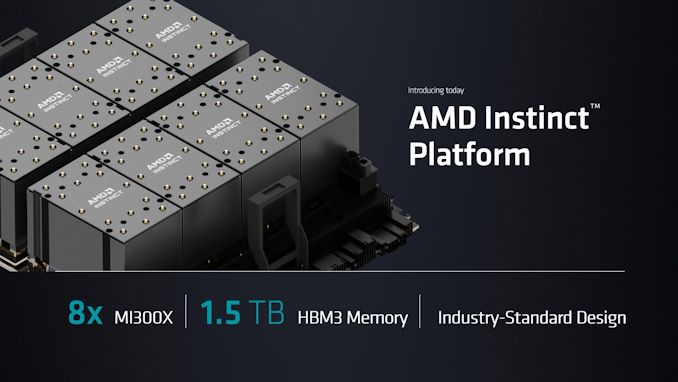
Alongside today’s 192GB MI300X news, AMD is also briefly announcing what they are calling the AMD Infinity Architecture Platform. This is an 8-way MI300X design, allowing for up to 8 of AMD’s top-end GPUs to be interlinked together to work on larger workloads.
As we’ve seen with NVIDIA’s 8-way HGX boards and Intel’s own x8 UBB for Ponte Vecchio, an 8-way processor configuration is currently the sweet spot for high-end servers. This is both for physical design reasons – room to place the chips and room to route cooling through them – as well as the best topologies that are available to link up a large number of chips without putting too many hops between them. If AMD is to go toe-to-toe with NVIDIA and to capture part of the HPC GPU market, then this is one more area where they’re going to need to match NVIDIA’s hardware offerings
AMD is calling the Infinity Architecture Platform an “industry-standard” design. Accoding to AMD, they're using an OCP server platform as their base here; and while this implies that MI300X is using an OAM form factor, we're still waiting to get explicit confirmation of this.


