Original Link: https://www.anandtech.com/show/18871/arm-unveils-armv92-mobile-architecture-cortex-x4-a720-and-a520-64bit-exclusive
Arm Unveils 2023 Mobile CPU Core Designs: Cortex-X4, A720, and A520 - the Armv9.2 Family
by Gavin Bonshor on May 28, 2023 8:30 PM EST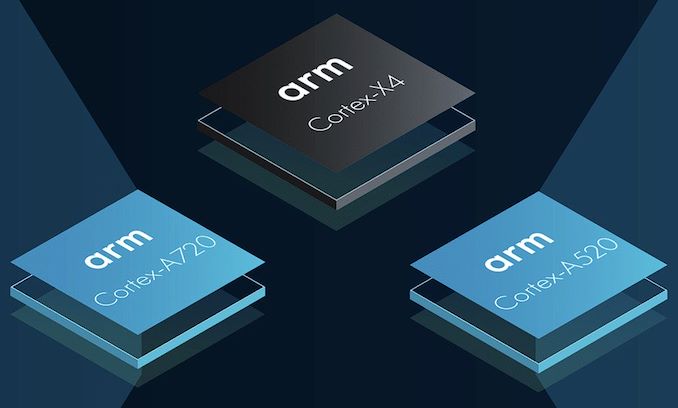
Throughout the world, if there's one universal constant in the smartphone and mobile device market, it's Arm. Whether it's mobile chip makers basing their SoCs on Arm's fully synthesized CPU cores, or just relying on the Arm ISA and designing their own chips, at the end of the day, Arm underlies virtually all of it. That kind of market saturation and relevance is a testament to all of the hard work that Arm has done in the last few decades getting to this point, but it's also a grave responsibility – for most mobile SoCs, their performance only moves forward as quickly as Arm's own CPU core designs and associated IP do.
Consequently, we've seen Arm settle into a yearly cadence for their client IP, and this year is no exception. Timed to align with this year's Computex trade show in Taiwan, Arm is showing off a new set of Cortex-A and Cortex-X series CPU cores – as well as a new generation of GPU designs – which we'll see carrying the torch for Arm starting later this year and into 2024. These include the flagship Cortex-X4 core, as well as Arm's mid-core Cortex-A720. and the new little-core Cortex-A520.
Arm's latest CPU cores build upon the foundation of Armv9 and their previous Total Compute Solution (TCS21/22) ecosystem. For their 2023 IP, Arm is rolling out a wave of minor microarchitectural improvements through its Cortex line of cores with subtle changes designed to push efficiency and performance throughout, all the while moving entirely to the AArch64 64-bit instruction set. The latest CPU designs from Arm are also designed to align with the ongoing industry-wide drive towards improved security, and while these features aren't strictly end-user facing, it does underscore how Arm's generational improvements are to more than just performance and power efficiency.
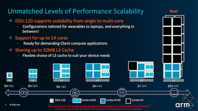
In addition to refining its CPU cores, Arm has undertaken a comprehensive upgrade of its DynamIQ Shared Unit core complex block, with the DSU-120. Although the modifications introduced are subtle, they hold substantial significance in terms of improving the efficiency of the fabric holding Arm CPU cores together, along with extending Arm's reach even further in terms of performance scalability with support for up to 14 CPU cores in a single block – a move designed to make Cortex-A/X even better suited for laptops.
With three new CPU cores and a new core complex, there's a lot to cover. So let's dive right in.
Arm TCS23 at a High Level: Pushing Efficiency & Going Pure 64-bit
Expanding on the enhancements introduced in the Armv9.1 architecture last year, Arm is progressing through its scheduled development cycle with the latest Armv9.2 architecture. The primary objective of this cycle is to eliminate support for 32-bit applications and transition to a comprehensive 64-bit platform. Underpinning this transition is Arm's strategic framework, "Total Compute Solutions" (TCS), which revolves around three core principles: compute performance, security, and developer access. This approach forms the foundation for Arm's methodology and guides its efforts in delivering optimal performance, robust security measures, and streamlined developer capabilities.
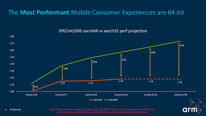
Arm's focus on phasing out the 32-bit instruction set has been one it has been working towards for several years. For their latest TCS23, they have finally created a fully 64-bit cluster to capitalize on the benefit of a complete 64-bit mobile ecosystem, excising AArch32 (32-bit instruction) support entirely.. So whether it's a big, mid, or little core, for Arm's latest generation of IP there is only AArch64.
Developing a dynamic system-on-a-chip (SoC) that caters to a broad spectrum of mobile devices, ranging from cutting-edge flagship smartphones to entry-level models, necessitates a meticulous and consistent approach to maintaining competitiveness in a rapidly expanding market. In the realm of flagship devices, for instance, Qualcomm's Snapdragon 8 Gen2 SoC stands out, leveraging a cluster of Arm's Cortex-X3, Cortex A715/710, and Cortex-A510 cores. The upcoming iteration of Qualcomm's Snapdragon 8 Gen3 and other SoC manufacturers are poised to harness the power of Arm's TSC23 core cluster and intellectual property to further enhance performance in the subsequent generation of flagship mobile devices.
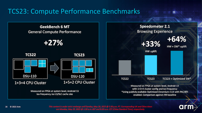
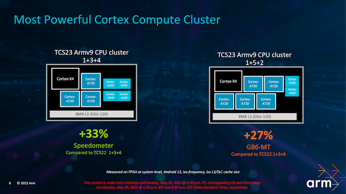
Arm's latest DynamIQ Shared Unit, DSU-120, offers support for up to 14 CPU cores in a cluster, which opens the door to a significant number of different CPU core combinations. We'll see what SoC vendors have opted for later this year, but one probably configuration is a 1+5+2 (X4+720+520), which is likely a configuration for a high-end smartphone. Compared to a last-generation 1+3+4 cluster (X3+715+510), Arm is claiming an uplift of 27% in compute performance within GeekBench 6 MT and a more considerable uplift of between 33% and 64% in the Speedometer 2.1 benchmark depending on software optimizations implemented.
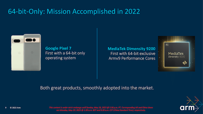
Focusing more on the approach to 64-bit migration, last year Arm announced their first AArch64-only CPU core, the Cortex-A715. Consequently, last year saw the release of the first 64-bit only products, such as MediaTek's Dimensity 9200 SoC, as well as Google's Pixel 7 – which was 64-bit only as a platform choice rather than an architectural restriction.
That said, actual AArch64 adoption/use within the larger software ecosystem has been slower than expected, primarily due to the Chinese market being slow to make the switch from 32-bit to 64-bit. Google has actually been key with its application storage (Google Play) by requiring its developers to submit 64-bit apps as far back as 2019, while also allowing the use of 32-bit applications on devices without native 64-bit support. Other markets haven't been as quick in doing so, but Arm claims that it is 'nudging' companies such as OPPO, Vivi, and Xiaomi to adopt AArch64 faster, which is believed to have the desired effect.
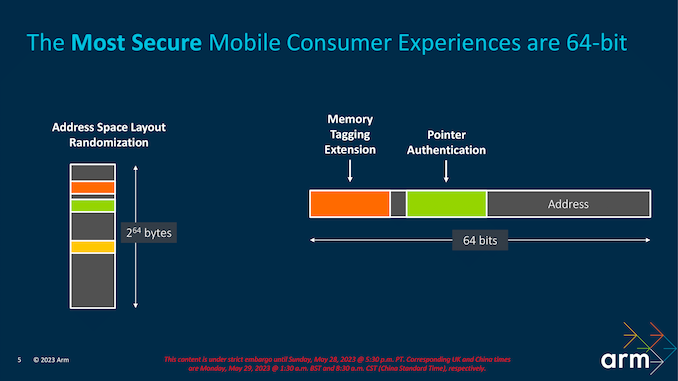
With the initial Armv9 architecture, Arm made improvements to security through the use of its Memory Tagging Extension (MTE) (Armv8.5), which is a hardware-based implementation that uses Pointer Authentication (PA) extensions to help protect from memory vulnerabilities. Memory-based vulnerabilities have been a consistent threat to hardware-based security for many years, and it is something Arm is continually developing within its IP to help mitigate these types of attacks. For reference, Google's Chromium Project claimed that around 70% of high-severity bugs are from memory.
One of the related security features of the latest Armv9.2 architecture is the introduction of a new QARMA3 Pointer Authentication Code (PAC) algorithm. Arm claims the newer algorithm reduces the CPU overhead of PAC to less than 1%, even on their little cores, giving developers and handset vendors even less of a reason to not enable the security feature. Most of these improvements revolve around hardware integrity and security, with a combination of MTE and native benefits through the 64-bit instruction and architecture, all designed to make devices even more secure going into 2023 and beyond. This fits with Arm's ethos to encourage a full switch to 64-bit over a hybrid 64 and 32-bit marketplace.
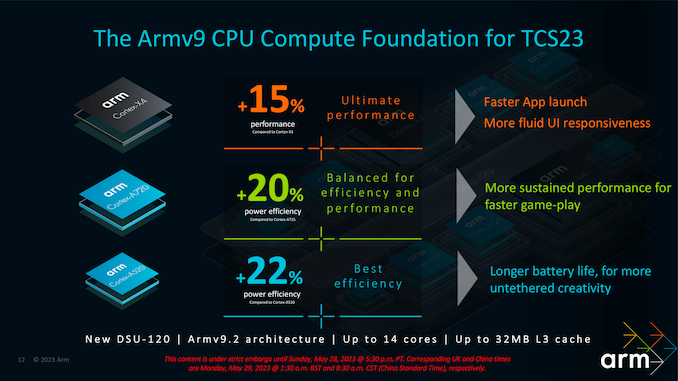
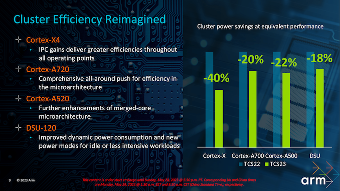
Finally, looking at performance, Arm claims that their latest generation CPU and core complex architecture has made solid gains in power efficiency. At iso-performance, Cortex-X4 offers upwards of a 40% reduction in power consumption versus Cortex-X3, while Cortex-A720 and A520 save 20-22% over their respective predecessors. On the DSU-120 hub itself, Arm claims an 18% improvement in power efficiency.
Of course, most of these power savings are going to instead be invested in additional performance. But it goes to show what SoC and handset vendors can aim for in this generation if they focus singularly on power efficiency and battery life.
Arm Cortex-X4: Fastest Arm Core Ever Built (Again)
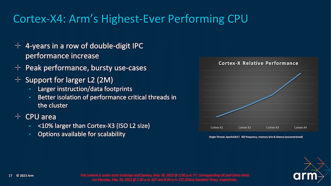
Diving further into Arm's new CPU core microarchitectures, we'll start with the Cortex-X4, which stands out as the most substantial advancement. Arm has consistently achieved significant double-digit improvements in instructions per cycle (IPC) with each iteration, starting from the original Cortex X1 core, then progressing to the Cortex X2, and continuing with the Cortex-X3 IP introduced last year, and they'll do so again for the Cortex-X4 in 2023 as well. The Cortex-X4 is specifically designed to cater to cutting-edge flagship Android-based smartphones and leading mobile devices that utilize robust Arm IP-based System-on-Chips (SoCs). Representing a subtle yet impactful enhancement over its predecessor, the Cortex-X4 further refines the capabilities of the Cortex-X3 core.
The Cortex-X4 is designed to deliver top-tier compute performance in mobile System-on-Chips (SoCs), particularly tailored to handle demanding workloads like AAA gaming and bursty operations. The Cortex-X4 is Arm's highest-performing core to date, featuring an anticipated core clock speed of 3.4 GHz and an increased L2 cache per core, doubling its capacity to 2 MB compared to last year's 1 MB Cortex-X3 . Despite these enhancements, Arm has managed to maintain a minimal increase in the physical size of the core, with the more complex X4 CPU core coming in at under a 10% die size increase (the additional L2 cache excluded).
As for power efficiency, Arm claims a notable improvement in power savings of approximately 40% compared to previous generations. Don't expect to see too many CPU vendors take advantage of that, since the primary job of the X-series is to run fast, but it goes to show what the X4 can accomplish in conjunction with the latest fab nodes.
Arm Cortex-X4: Front End Reshuffle, Redesigning Instruction Fetching
In terms of architecture, the Cortex-X4 exhibits similarities to its predecessor, the Cortex-X3, with the primary focus being on refining the existing architecture and optimizing efficiency across various core components.
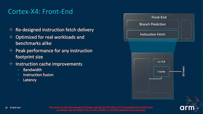
Now while things haven't changed all too much architecturally from the Cortex-X4 to the Cortex-X3, the Cortex-X4 front end has had a reshuffle and a tweak of the instruction fetching block. The aim of Arm has been to keep latencies low while offering peak bandwidth throughout its Cortex-X4 core and within the entire TSC23 core cluster.
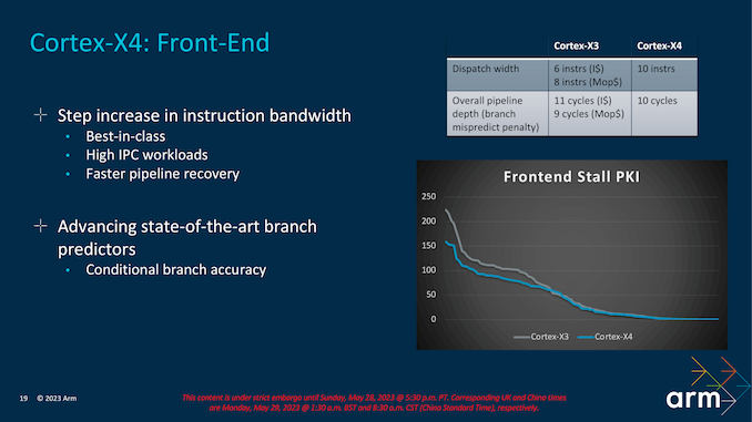
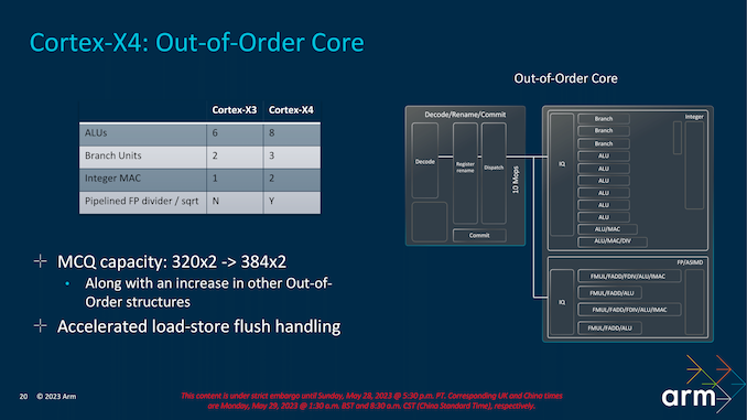
With regards to the Cortex-X4's front end, the big architectural change here has been through its dispatch width. The Cortex-X4 now has a more focused 10-wide dispatch width, up for the 6/8-wide dispatch width of the X3. That said, while the front-end has gotten wider, the effective pipeline length has actually shrunken even so slightly; the branch mispredict penalty is down from 11 cycles to 10.
The other big front-end focus has been on the instruction fetching process itself; Arm has essentially redesigned the entire instruction fetch delivery system to ensure better efficiency throughout the pipeline when compared to the Cortex-X3.
The latest architecture also takes another pass on improving Arm's branch prediction units, further improving their prediction accuracy. Arm isn't saying much about how they accomplished this, though we do know that they've targeted conditional branch accuracy in particular. None of this comes for free, though; Arm was quick to note that the improved predictors were more expensive to implement. Still, Arm believes this is worth it in keeping the beast (Cortex-X4) fed, so to speak.
Shifting to the back-end of the CPU core, Arm has taken a focus on execution bandwidth. Among other changes, Arm has increased the number of ALUs from 6 to 8. Of these, six are simple ALUs for processing single-cycle uOPS. Meanwhile, there are two complex ALUs for processing dual and multi-cycle instructions, Arm has also squeezed another branch unit in, giving the Cortex-X4 a total of 3, up from 2, as well as adding an extra Integer MAC. Meanwhile on the floating point side of matters, the Cortex-X4 also upgrades a pipelined FP divider.
So to some extent, the X4's performance improvements come from a brute force increase throughout the chip, with the chip able to dispatch and retire more instructions in a single clock. The goal for the Cortex-X4 is to offer peak performance on both benchmarks and real-world workloads, as well as an increase in the fetch bandwidth for any instruction set going through the pipeline. The benefits come through latency reductions and instruction fusion benefits for larger instruction footprint workloads.
Increasing the Micro-op Commit Queue (MCQ) capacity – and thus the size of the window for instruction re-ordering – is another refinement in Arm's toolbox for Cortex-X4. As with previous increases in Arm's re-order buffers, the larger queue affords more opportunities to look for instruction re-ordering, to hide memory stalls and otherwise extract more opportunities for the rest of the CPU back-end to get some work done. And with CPU performance continuing to outpace memory bandwidth, the need for larger buffers only grows with each generation.
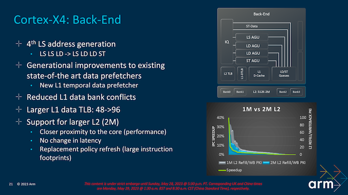
Finally, at the far back end of the X4 CPU core, Arm has added a fourth address generation unit. Interestingly, this one is just for stores; Arm already had a load-only unit, but opted for a store-only unit rather than converting it to a full mixed LS unit.
The L1 cache subsystem of the Cortex-X4 has also received a lot of work. The L1's translation lookaside buffer (TLB) has been doubled to 96 entries, and there's a new L1 temporal data prefetcher. Finally, Arm has taken steps to reduce the number of L1 data bank conflicts on the X4.
There have also been some changes made to better support the larger L2 cache size of the Cortex-X4 that we previously discussed. The L2 has been moved physically closer to the CPU core for performance reasons, and Arm has been able to expand the L2 size without any resulting increase in latency. So there is less of a trade off here than is often the case for increasing cache sizes.
Cortex-X4: IPC Uplift, Scalable up to 14-Cores, Up to 32 MB L3 Cache
One of the primary benefits of Arm's v9.2 architecture shift is that it offers increased scalability. The TSC23 core cluster now supports up to 14 cores which adds a level of flexibility for SoC vendors to implement into their latest designs. Perhaps one of the biggest changes is support for up to 32 MB of shared L3 cache within the TSC23 core cluster. The levels of L3 cache implemented is of course down to the SoC manufacturer, but the maximum levels that can be offered is 32 MB, which allows increased support for higher-end mobile devices such as tablets and notebooks, where applicable.
The maximum number of cores across the entire TSC23 core cluster stretches to 14 in total, with a mixture of big and little cores, with multiple avenues for SoC vendors to explore to capitalize on things like performance gains and efficiency. All of this flexibility is given to the SoC vendors to design their own variations depending on the level of the device. So a flagship mobile device will leverage different combinations of Cortex-X4, Cortex-A720, and Cortex-A520 depending on multiple factors such as cost, power budget, and expected performance levels.
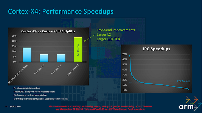
A bigger core and optimizations of existing processes typically come with a performance benefit. Arm is claiming that, based on its pre-silicon simulation numbers, the Cortex-X4 will deliver a 15% IPC uplift at iso-frequency and iso-bandwidth versus the Cortex-X3 used in last year's flagship Android SoCs. There are a number of factors at play here in delivering that total performance improvement, including front-end optimizations and improvements, as well as a larger L2 per core cache of 2 MB and a larger L1D-TLB, which is a cache designed for recently accessed page transitions.
Cortex-A720: Middle Core, Big on Efficiency
Focusing on Arm's latest middle core, the Cortex-A720 hasn't changed much from the previous Cortex A715 design last year, which was also Arm's first AArch64-only middle core. Arm has a set philosophy for its A700 family, and that's mostly about increasing performance through optimizations, delivering maximum levels of power efficiency within set thermal limits, and optimizing workloads for actual use cases instead of blisteringly fast benchmark performance. Arm's key aims are to enhance performance metrics while maintaining power efficiency, area, and all within an acceptable thermal envelope. Cost is also essential, with many entry-level mobile devices already on the market leveraging the Cortex A700 family for its main cores.
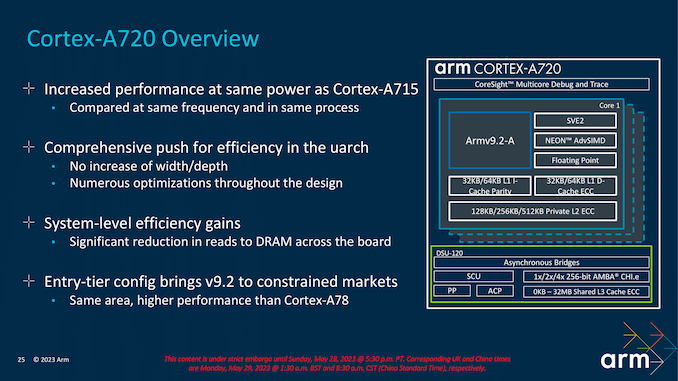
Similar to the Cortex-X4 in that the Cortex-A720 is built around the Armv9.2 ISA, Arm has optimized its design to enable the A720 to deliver more performance within the same power budget compared to the Cortex A715. The Arm 700-series family typically covers a much broader range of applications and caters to various markets, including, and not limited to, digital TVs (DTV), smartphones, and laptops. Having more comprehensive flexibility in a more diverse space has its advantages, and Arm looks to capitalize on that with the Cortex-A720 acting as the 'workhorse' of the TSC23 core cluster.
Devices such as smartphones at the entry-level typically want to reduce cost but maximize performance and efficiency, and that's where cores such as the Cortex-A720 come into play; the Cortex-X4 is primarily allocated to devices with flagship status or those that require the most burst and sustained performance, such as top tier smartphones, tablets, and laptops. Meanwhile, Cortex-A720 is the next step down, giving up the X4's high peak performance for a much smaller core size and with correspondingly lower energy consumption.
For the Cortex-A720 in particular, Arm is also offering multiple configuration options. Along with the standard, highest-performing option, Arm has what they're terming an "entry-tier" configuration that shaves A720 down to the same size as Arm Cortex-A78, all while still offering a 10% uplift in overall performance. With some Arm customers being especially austere on die sizes, moves such as these are necessary to convince them to finally make the jump over to the Cortex-A7xx series and Armv9.
Arm's focus is to broaden the range of the entry-level market and expand on the possible use cases for its Cortex-A720 core so that it can be implemented into a wider variety of entry-level mobile devices and in lower-end markets.
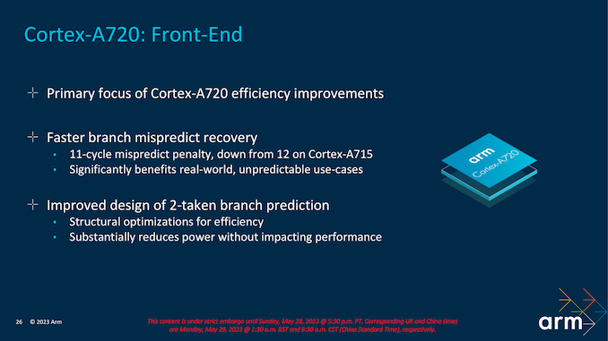
Some of the critical improvements to the Cortex-A720, when compared to the previous A715, is Arm has opted for a faster branch mispredict recovery. Branch prediction breaks down the instructions into predicates, and a branch predictor will only execute statements it predicates to be true. Opting for a faster branch mispredict recovery has multiple benefits, as it not only reduces the delay within the execution of instructions, but it can improve overall performance. Another element of this is pipeline efficiency, as a branch misprediction can disrupt the flow of instruction throughout the pipeline, and the ability to do this faster not only yields benefits to performance but also to overall power efficiency.
Arm has reduced the overall branch mispredict penalty on A720 to 11 cycles, down from 12 on the Cortex A715. They have also improved upon their 2-taken branch prediction technique, which predicts the outcome of the instruction, and, again, adds efficiency to the pipeline and reduces the penalties regarding misprediction.
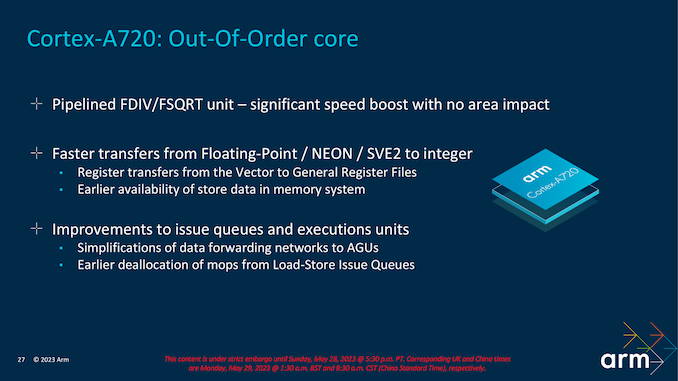
Another improvement is the Pipelined FDIV/FSQRT (division + square root), which performs operations on floating point numbers using the pipelines. Allowing for concurrent executions of both FDI and FSQRT can improve instruction throughput, and Arm claims to have achieved a significant speed boost without impacting the overall area. There are also faster transfers from floating point to floating point, including NEON and SVE2 integer, which Arm introduced for Armv9. This also includes overall improvements to issue queues and the execution units, which simplifies the forwarding of data forwarding to AGUs.
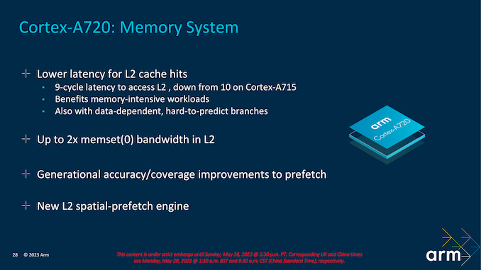
Within the memory system of the Cortex-A720, reduced the L2 cache latency to 9-cycles, and Arm claims to have up to 2x the memset(0) bandwidth within the L2 cache. Without going into much detail about their methods, Arm also claims to have improved generationally on accuracy and coverage to the prefetcher. However, it has a new L2 spatial prefetch engine, which was previously a pioneering Cortex-X core system design feature.
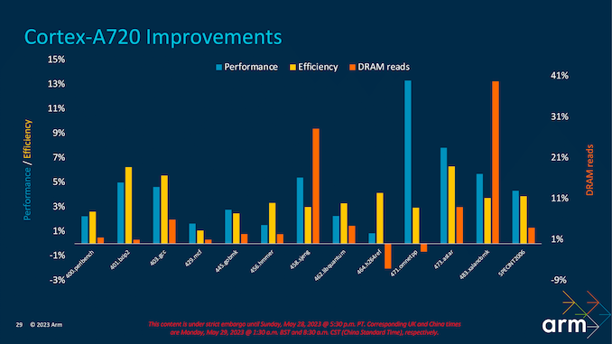
Translating the refinements and improvements to performance, Arm estimates the performance uplift to be about 15% at iso-frequency, depending on the workload. Among other benchmarkmarks, thare are clear gains over the previous generation in SPECint2017 and improvements within internal testing with SPECint2006. For example, using SPECint2007 as its performance indication metric in SPECint2007_403.gcc, the Cortex-A720 has a gain of around 5% over the Cortex A715, with an even more significant improvement of about 6% in power efficiency.
Other performance metrics on offer include DRAM reads, which Arm has focused a lot of attention on making more efficient, showing minor gains overall; SPEC2007int_483.xalacbmk shows a massive increase of up to 41% in DRAM read performance. While everything is relative and subjective to the workload tasked, Arm has made some clear forward progress with its latest Cortex-A720 CPU core microarchitecture.
Cortex-A520: LITTLE Core with Big Improvements
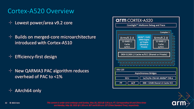
The third of the Armv9.2 cores is the Cortex-A520, which is little in design, but Arm promises big improvements over previous generations, particularly on power efficiency.
Addressing the biggest question right off the bat: no, Cortex-A520 is not an out-of-order core design. True to Arm's little core design ethos, it's still an in-order core – and in fact, Arm has even removed an ALU in the process.
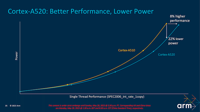
Arm's smallest core for this generation is a new core in effect, but it is still more of a refinement of the Cortex-A510 than a completely new design. It has the lowest power-to-area ratio of all three announced Cortex Armv9.2 cores. The most significant differences come through optimizations on power, with Arm claiming that the Cortex-A520 is 22% more energy efficient than the previous Cortex-A510 core at iso-process and iso-frequency. The little core in Arm's TCS23 catalog is primarily designed for performing low-intensity and background operational tasks, which takes these loads off bigger cores such as the Cortex-A720/Cortex-X4 to allow better power efficiency overall within the cluster.
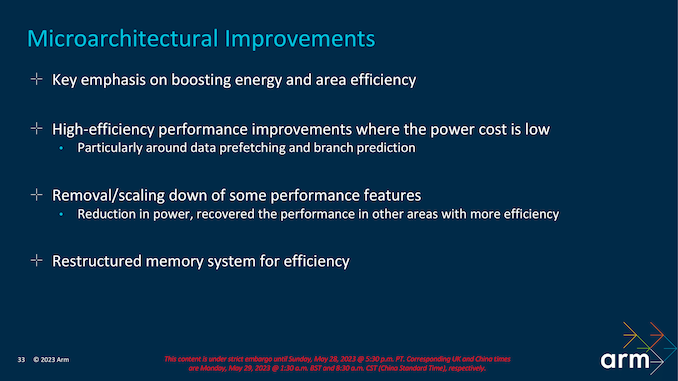
Many of Arm's efficiency gains come from small, microarchitectural level changes, mostly around how it implements data prefetch and branch prediction. On the whole, not much has been changed to the little core, but the small changes that have been made have all been about improving efficiency.
One of the non-architectural areas of improvement has been introducing the new QARMA3 Pointer Authentication Code (PAC) algorithm, which Arm claims to reduce PAC's overhead to under 1%. QARMA3 is a cryptographic-based technique designed to ensure the pointers' integrity is correct and accurate. It also provides a secure and efficient way to avoid tampering with the necessary underlying code so that any authorized modifications or tampering if the pointers are eliminated adds a layer of hardware-level security. Arm is not only leveraging QARMA3 PAC to boost security and integrity, but it also allows them to squeeze out additional levels of efficiency, if compared to using PAC with older algorithms.
Much like when Arm announced its armv9 architecture in 2021, the small Cortex-A520 cores can be merged in pairs to share pipelines and improve efficiency. Adopting a pairing of the smaller Cortex-A520 cores can enhance efficiency by combining them through relevant pipelines such as SVE, NEON, and FP. More so in the case of SVE2, which does require a larger area footprint than other executions and makes sense to pair two smaller cores than have just one on its own. However, it is entirely plausible and possible for SoC vendors to use single-core option implementations on their designs if they wish to do so.
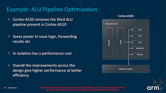
Sometimes less is more, and in the case of the Cortex-A520, Arm has removed the third ALU pipeline, which it originally added to the Cortex-A5x DNA with the Cortex-A510. Arm's ideology behind this is it saves power in issue logic and improves forwarding results within the overall complexity of the pipeline. In practice, Arm has figured out how to recover enough of the lost performance through other improvements that they are opting to eat the hit from removing the ALU in order to minimize core size and maximize efficiency.
Ultimately, Arm is looking at a big-picture trade-off as well; reducing the power consumption of the Cortex-A520 frees up energy that can be allocated to the other cores, such as the Cortex-A720 and even the Cortex-X4 where applicable. This makes Armv9.2 IP versatile and scalable, making small savings where it can deliver the savings in other areas where and when it is needed.
Using SPEC2006_int_rate_1copy as its performance metric to judge performance and efficiency, generation on generation (and at iso-process and iso-frequency), Arm is claiming the Cortex-A520 delivers 8% more performance than the Cortex-A510 at similar levels of power consumption. Alternatively, at iso-performance, Cortex-A520 can deliver a significant 22% power savings.
While seemingly small, it can add up in the grand scheme of things, especially across a four-core complex of Cortex-A520 cores. Although there's always a diminishing level of returns in terms of increasing core count when it comes to performance, having lower-powered and more efficient cores typically creates more power for other areas to tap into, such as the big Cortex-X4 core, which requires more grunt to boost those intensive and burst reliant workloads.
New DSU-120: More L3 Cache, Doubling Down on Efficiency
For the launch of its Armv9.2 architecture, Arm has decided to opt for a new core complex design for its TCS23 CPU cores by building upon the foundations of its current DSU-110 block. Initially introduced in 2017 along with the Cortex A75 and A55 cores, DSU-110 represented a significant redesign and generational shift to integrate larger pools of shared L3 cache, bandwidth, and scalability. Along with the efficiency tweaking Arm has done to its new Cortex-X4, Cortex-A720, and A520 cores, the new DynamIQ Shared Unit-120 (DSU-120) also plays a significant role in these advancements.
Building a more refined DSU instead of another ground-up design, Arm has made plenty of inroads to improving overall scalability, efficiency, and performance with its DSU-120. Some of the most notable improvements include support for up to 14 CPU cores in a single cluster, which allows SoC vendors to pick and choose their core cluster configurations to suit the device going to market. Arm has also improved its Power and Performance Area (PPA) by implementing new power-saving modes, including RAM and Slicing power-downs, which work in stages depending on the type of workload and the intensity to reduce the overall power footprint of the cluster.
Perhaps the most significant change to DSU-120 from DSU-110 is that Arm has effectively doubled the total amount of shared L3 cache a cluster can implement. DSU-110 initially supported up to 16 MB, whereas DS-120 can now accommodate up to 32 MB of shared L3 cache across the entire complex, with other options also available, including 24 MB. While this isn't a direct implementation into the IP, the decision on the number of L3 cache implemented is entirely down to SoC vendors to decide the right levels of L3 cache based on performance and efficiency balancing depending on the device. The key focus is that DSU-120 and the new TCS23 cluster have the ability to support this if vendors wish to implement more L3 cache.
As with the current/previous DSU-110 interconnect, the new DSU-120 also uses a dual bi-directional ring-based topology, which allows data transmission in both directions within the cluster and reduces overall latency. The overall design of the DynamIQ Shared Unit is to optimize things for latency and increase bandwidth, which is precisely what Arm has done by slicing its logic L3 and snoop filters. As such, it is configurable based on specific customer bandwidth requirements. As previously mentioned, DSU-120 allows up to 14 Cortex-X/A cores to be implemented into a cluster, with plenty of benefits of opting for the latest Armv9.2 generation over the previous iterations.
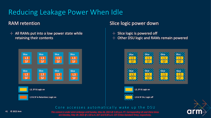
Focusing on the new power improvements to the TCS23 and DSU-120 complex, Arm has identified specific areas where it can save on power to maximize efficiency. One of these is through RAM and reducing any unnecessary power leakage associated with that. To combat this, Arm has opted for a mechanism that allows RAM to be placed into a low-powered state when not being actively used, but still with enough power to ensure the integrity of its contents. The Logic is split into slices with the L3 cache and a snoop filter designed to improve cache coherence within a multi-core complex.
Opting for a sliced approach with snoop filters enables a couple of things. Firstly as we've mentioned, it improves and enhances cache coherence. This means that the cores are fed consistently and up-to-date instructions, and the snoop filter itself is designed to filter out requests that are deemed unnecessary, which does give some efficiency benefits. Secondly, slicing allows Arm's IP to increase scalability, which with an increase in cores, means an increase in slices with dedicated cache slices, allowing for better distribution of data and lower data contention rates. Armv9.2 IP with the DSU-120 allows for between 1 and 8 slices to be used, designed to enable SoC vendors the flexibility to work within their bandwidth requirements.
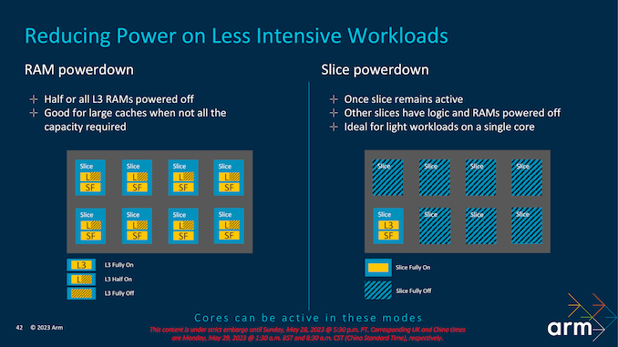
Arm claims that RAM power-down enabled across half of the L3 RAMs on the complex is suitable for large L3 caches when all of the capacity isn't being used. By allowing RAM power-down, all of the unused RAM is put into a low power state, but with enough to keep the contents and withhold their integrity within the memory substructure. Even with RAM and Slice power-downs active, the cores can still be active and process relevant instructions and data. One slice will effectively remain active, which is ideal for smaller and light workloads on a single core, but when it comes to powering down features on the DSU-120 interconnect, accessing the cores will enact a wake-up of the DSU-120.
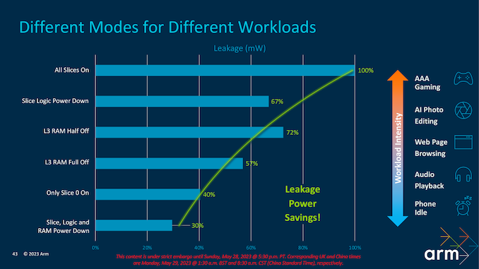
Looking at how this efficiency translates into data, Arm has provided a handy slide with estimates from its own testing. As we can see, with various levels of RAM and Slice Logic power-downs, we get varied potential power savings, which can then be budgeted back into the cores themselves for higher performance levels. Different workloads and tasks require different levels of core power, coherence, intensity, and L3 allocation, so different power-downs lead to varying levels of leakage and power efficiency savings. Arm's figures estimate between 30 and 72% at the other states of power-down, with 100% savings in leakage with all the slices enabled.
Closing Remarks: TCS23 Promises Improved Performance and Power Efficiency
Coming from Arm's latest client technology day, my impression is that this is a generation where, even more so than usual, Arm's primary focus is on improving their power efficiency. Much of the focus on the latest cores, including the large Cortex-X4, the middle Cortex-A720, and the little Cortex-A520, isn't about reinventing the wheel, but more about greasing it to squeeze out improvements versus their previous Armv9-based microarchitecture. All the while, Arm has also gone the whole nine yards in ensuring SoC vendors and the broader market are prepared for a complete and dynamic switch from the current hybrid 64/32-bit mobile market to a full AArch64 world.
Comparing TCS22 to TCS23 with an identical core complex configuration of 1+3+4, Arm claims significant gains using the Speedometer benchmark of up to 33% at iso-frequency. Elsewhere, things get slightly skewed when Arm compares their latest TCS23 cluster with a 1+5+2 configuration against TCS22 with 1+3+4. Still, Arm is claiming a 27% improvement in GeekBench 6's Multi-threaded benchmark across the board, where opting for two larger middle cores and losing two smaller cores has a major impact on that figure.
The critical takeaway from Arm's Armv9.2 announcement is that their IP is going fully bound towards an entire and complete 64-bit ecosystem, and they are looking to harness all of the benefits from a more unified marketplace.
Even though from a technical standpoint, the refinement of its existing TCS22 IP for all of the efficiency gains they bring isn't avante-garde. It's more about refining the current IP to align with a broader market focus on efficiency. From what we can see, much of the gains have come from reducing specific power structures through implementations such as RAM power down and Slice power down to save energy where it can and allow the power saved to be used in other areas; or not at all to save on device battery life.
Arm has further improved its energy efficiency across implementations of all of its three new cores, the Cortex-X4, the fastest core Arm has ever created, down to the middle Cortex-A720 and little Cortex-A520 core. Finding power and performance gains in each of these cores adds to a much more significant effect on overall efficiency, precisely what Arm has been doing for many years. Even the latest DynamIQ Shared Unit (DSU-120) has implementations active through the use of dynamic power consumption and various power modes for idle, which makes things more efficient from a performance point of view, especially if the workload isn't intensive and can be allocated to the right cores and specific slices of logic can be powered down to maximize efficiency.
Meanwhile, the shift to the pure, 64-bit only AArch64 ISA yields many improvements in different areas. For Arm's IP teams, it allows Arm to focus its efforts directly on one specific ISA as we advance. Still, it also enables parity within its software, in which Arm's software engineering staff comprises 45% of its overall engineering team. That's a serious chunk of manpower working on making refinements within the gap between software, hardware, and IP, and one that is driving the 64-bit ISA ecosystem further toward a completely unified market space. The performance benefits and security-based ones are prevalent within the jump between 32-bit and 64-bit, it's just adopting a unified system, and Arm is undoubtedly encouraging a market shift from previous products, including the newly announced Armv9.2 architecture.
While Chinese companies such as OPPO have been notoriously slow in making these moves into 64-bit, the uptick in 64-bit applications within the Chinese market has grown exponentially over the last year. The application cycle between 64-bit and 32-bit has been primarily driven by Google and its Play Store, with its developers needing to compile a 64-bit version for many years. This requirement ensures that software developers, especially those partnered with Arm to optimize their software for the latest Arm IP, are having a positive effect on slower adopters and markets, pushing them to finally make the switch to 64-bit.
The next step for 64-bit is squeezing out more advantages over 32-bit; for one, security plays an even more significant part in driving things forward. Not only does AArch64 outperform AArch32, but the 64-bit ISA provides for more security options. And finding efficiencies in streamlining the whole process from IP to hardware, to software, to the device, to market, is one that should hopefully reduce costs by dropping 32-bit entirely from companies plans. Even for devices such as the next wave of Digital TVs (DTV), which is a growing market, these vendors can undoubtedly apply the benefits of both increased performance and security integrity to their products.
All of this goes hand-in hand with the manufacturing side of things, as well. For as much as Arm has improved its designs at the IP level, and delivering gains on an iso-process basis, node shrinks are still the most potent way to improve chip performance, especially when it comes to energy efficiency. That Arm's TSC23 IP is the first IP to tape out on TSMC's N3E process is no fluke, and it marks the final ingredient of Arm's PPA design philosophy.
Overall, while Arm's 2023 CPU and system IP don't bring any radical microarchtectual changes at any one level, on the whole it's a solid slate of new IP offerings. After getting the ball rolling on the swtich to pure 64-bit CPU cores with Cortex-A715 last year, this year's final and full shift will still take some getting used to, but it should be a pretty smooth transition overall. And by doing this at the same time as focusing on those aspects of PPA that their SoC customers really care about – small die sizes that keep down energy consumption – Arm is giving their partners two very good reasons to keep moving forward with the rest of the company. Just what kind of chips Arm's partners ultimately build remains to be seen, but we are looking forward to seeing how things pan out later this year.

