Original Link: https://www.anandtech.com/show/17032/tensor-soc-performance-efficiency
Google's Tensor inside of Pixel 6, Pixel 6 Pro: A Look into Performance & Efficiency
by Andrei Frumusanu on November 2, 2021 8:00 AM EST- Posted in
- Smartphones
- Mobile
- SoCs
- Pixel 6
- Pixel 6 Pro
- Google Tensor
It’s been about two weeks since Google officially announced their newest flagship devices in the form of the Pixel 6, and Pixel 6 Pro. The two new Pixel phones are inarguably Google’s largest shift ever since the Pixel series was introduced, showcasing major changes in essentially every aspect of the devices, sharing very little in common with their predecessors besides the Pixel name. Featuring brand new displays, camera systems, body designs, and internal hardware at seemingly extremely competitive pricing, the phones seem to be off to an extremely good start and competitive positioning Google hasn’t had in a long time.
One of the biggest changes, and most interesting to our readers, is the fact that the Pixel 6 and Pixel 6 Pro come powered on by Google’s own “Tensor” SoC. And it’s here where there’s quite a bit of confusion as to what exactly the Tensor is. Google explains that the Tensor is Google’s start in a journey towards the quest of enabling new kinds of workloads, which in the company’s words, were simply not possible or achievable with “standard” merchant silicon solutions. Taking advantage of Google research’s years of machine learning experience, it’s a chip that’s heavily focused towards ML as its primary differentiating feature, and what is said to allow the Pixel 6 phones to have many of the new unique feature exclusive to them.
Today, we’re giving the Tensor SoC a closer look. This includes trying to document what exactly it’s composed of, showcasing the differences or similarities between other SoCs in the market, and better understanding what kind of IPs Google has integrated into the chip to make it unique and warrant calling it a Google SoC.
The Chip Provenance
Officially, per Google’s own materials, the Tensor is a Google SoC fully designed by the company. And while the overall truth of this will vary based on your definition of “design”, the chip follows a seemingly close cooperation between Google and Samsung LSI, in the process blurring the lines between a traditional custom design and semi-custom design-for-hire chips such AMD’s console APUs.
Starting off at the very highest level, we have the actual name of the SoC. “Google Tensor” is quite abstract in that, for the time being, the chip doesn’t have any particular model number attached to it in terms of official marketing. So whether the next-gen will be marketed “Tensor 2” or something else will remain to be seen. Internally, Google calls the chip the “GS101”, and while I’m not entirely sure here what GS stands for, it’s likely Google SoC or Google Silicon. For quite some time now we’ve also heard the “Whitechapel” being reported, although I’ve seen no evidence that this was a reference to the actual chip but in the very early stages.
On the silicon side, the chip has another model number, with the SoC’s fused chip identification following Samsung’s Exynos naming scheme. Here we find the chip has an ID of “0x09845000”, which corresponds to what would be S5E9845 (Edit: It's actually S5P9845). The latest Samsung LSI SoC, for reference, is the Exynos 2100, which is identified as the S5E9840.
Of course, why would the Google SoC follow an Exynos internal naming scheme? That’s where we can begin to see some of the provenance of the design. It’s been widely reported for some time that a few years back, Samsung opened up itself to semi-custom silicon design offers. A piece from August 2020 from ETNews seems to correctly describe Samsung’s business plan and how it pertains to the Google chip (as well as describing a Cisco design win):
“Samsung Electronics is set to manufacture semiconductor chips for Cisco Systems, which is the top network equipment maker in the world, and Google and it is responsible for the entire semiconductor manufacturing process from design to production.
[…]
Samsung Electronics is currently working on a development phase that involves chip design.
[…]
Samsung Electronics also obtained an order from Google regarding manufacturing of more than one chip. It is heard that Google requested a semiconductor that will go into a sensor that can measure body movements rather than for processors that go into current IT devices and an unprecedented application processor (AP).
[…]
Samsung Electronics is carrying out a different approach as it looks to actively utilize its technologies in chip design. Its strategy is to provide “customized” technologies and features that its customer needs even from a design stage and secure consignment production as well.
What’s important here is the latter description of the process – where rather than simply acting as a pure-play contract manufacturer, Samsung is acting as a fully engaged party in the design of the silicon. This could very much be compared to an ASIC design service, with the exception being that Samsung is also a merchant SoC vendor as well as a manufacturer for the silicon, something that’s quite unique in the industry, and thus something of a special situation.
Having the chip in our hands now, as well as having the open-source insight into the characteristics of it, we can start breaking down what exactly the Google Tensor is:
| Google Tensor and Samsung Exynos 2100: Similar But Different | |||
| SoC |
Google Tensor |
Exynos 2100 |
|
| CPU | 2x Cortex-X1 @ 2.80GHz 2x1024KB pL2 2x Cortex-A76 @ 2.25GHz 2x256KB pL2 4x Cortex-A55 @ 1.80GHz 4x128KB pL2 4MB sL3 |
1x Cortex-X1 @ 2.91GHz 1x512KB pL2 3x Cortex-A78 @ 2.81GHz 3x512KB pL2 4x Cortex-A55 @ 2.20GHz 4x64KB pL2 4MB sL3 |
|
| GPU | Mali G78 MP20 @ 848 MHz (shaders) 996 MHz (tiler / L2) |
Mali G78 MP14 @ 854 MHz |
|
| Memory Controller |
4x 16-bit CH @ 3200MHz LPDDR5 / 51.2GB/s 8MB System Cache |
||
| ISP | Hybrid Exynos + Google ISP | Full Exynos ISP Blocks + DSP |
|
| NPU | Google edgeTPU @ 1066MHz |
Exynos NPU @ 1352MHz |
|
| Media | Samsung Multi-Function Codec 8K30 & 4K120 encode & 8K60 decode H.265/HEVC, H.264, VP9 AV1 Decode |
||
| Google "BigOcean" 4K60 AV1 Decode |
|||
| Modem | Exynos Modem 5123 External (LTE Category 24/18) (5G NR Sub-6) (5G NR mmWave) |
Exynos Modem 5123 Integrated (LTE Category 24/18) (5G NR Sub-6) (5G NR mmWave) |
|
| Mfc. Process | Samsung 5nm (5LPE) |
||
Same Blood Type
In the very fundamentals of what an SoC is, the Google Tensor closely follows Samsung’s Exynos SoC series. Beyond the usual high-level blocks that people tend to talk about in an SoC, such as CPUs, GPUs, NPUs, and other main characteristics, there’s the foundational blocks of a chip: these are the fabric blocks and IP, the clock management architecture, power management architecture, and the design methodology of the implementing those pieces into actual silicon. While on paper, a Samsung Exynos, a MediaTek Dimensity or a HiSilicon Kirin, or even a Qualcomm Snapdragon (on the CPU side) might have similar designs in terms of specifications – with the same high-level IP such as Cortex CPU or Mali GPUs from Arm – the chips will still end up behaving and performing differently because of the underlying SoC architecture is very different.
In the case of the Tensor, this “chassis” builds upon the IP Samsung uses on their Exynos SoCs, utilizing the same clock management and power management architecture. Going further up in the IP hierarchy we find additional similarities among high-level IP blocks, such as memory controllers, fabric IP, PHY IP for all kinds of externally facing interfaces, and even the larger IP functional blocks such as ISP or media decoders/encoders. The fun thing is that these things are now publicly scrutinizeable, and can be compared 1:1 to other Exynos SoCs in terms of their structures.
This leads us to Google’s claim of the Tensor being their own design – which is true to an extent, but how true that is can vary based on your definition of “design” and how in-depth you want to go with that. Although the Tensor/GS101 builds upon Exynos foundational blocks and IPs – and likely was even integrated and taped-out by Samsung – the definition of the SoC is in Google’s control, as it is their end-product. While things are very similar to an Exynos 2100 when it comes to Tensor’s foundation and lowest level blocks, when it comes to the fabric and internal interconnects Google’s design is built differently. This means that the spiderweb of how the various IP blocks interact with each other is different from Samsung’s own SoC.
A practical example of this is how the CPU cores are integrated into the SoC. While on the Exynos 2100 the CPU cluster seemingly lies very clearly in a smaller, more defined Samsung Coherent Interconnect, the Tensor SoC integrates the CPU clusters in a larger CCI that appears to either be a very different configuration of the interconnect setup, or is a different IP altogether. Meanwhile there are still some similarities, such as having one predominant memory traffic bus connected to the memory controllers and one other lower-traffic “internal” bus for other IPs, which is how Exynos SoCs tend to separate things. It should be possible to reverse-engineer and map out the SoC in more detail, however that’s a time-consuming matter out of the scope of this piece.
The CPU Setup - 2x X1 + 2x A76 + 4x A55
While we could go on and on talking about SoC architecture, let’s curtail that for now and jump into the more visible and practical differences of the Tenor SoC, starting off with the CPU cluster.
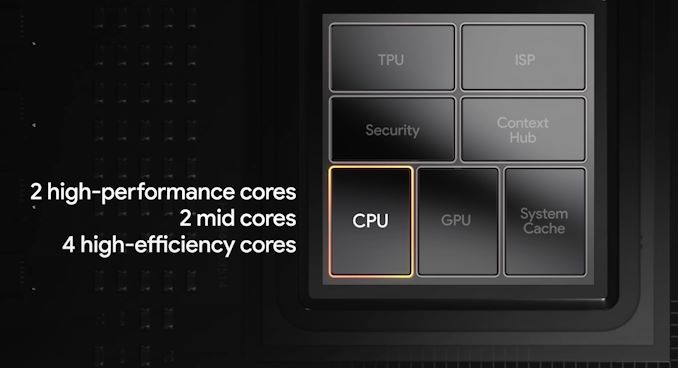
Google’s CPU setup is quite unusual from other SoCs in that it features a 2+2+4 configuration. While this isn’t truly exceptional – Samsung had this very same setup for the Exynos 9820 and Exynos 990 – the X1+A76+A55 configuration on the Tensor is currently unique in the market. Most other vendors and implementations out there have shifted over to a 1+3+4 big+mid+little CPU configurations.
On the Cortex-X1 side, Google’s use of a pair of cores means that, in theory, the performance of the chip with two heavy threads should be higher than any other Android SoC which only have a single big large performance core. The frequencies of the X1 pair come in at 2.8GHz, slightly lower than the 2.86GHz of the Snapdragon 888 and 2.91GHz of the Exynos 2100 X1 cores. Google equipped the cores with the full 1MB of L2 cache, similar to the S888 and double that of the E2100 configuration.
As for the middle cores, Google has employed Cortex-A76 cores, which has been a hot topic for discussion. At first glance, it’s seemingly a bit irrational considering both the Cortex-A77 and A78 offer higher performance and higher energy efficiency. The cores are clocked at 2.25GHz and come with 256KB of L2. We haven’t received a clear explanation from Google as to why they used the A76, but I do think it’s likely that at the time of design of the chip, Samsung didn’t have newer IP ready for integration. The chip has been brewing for some time and while it does feature X1 cores, maybe it was too late in the process to also shift over to newer middle cores. I do not think there was a purposeful choice of using A76 cores instead of A78, since as we’ll see in our performance benchmarks that the older design underperforms.
On the little cores, there are 4x A55 cores at 1.8GHz. In contrast to Samsung’s own Exynos chips, Google has decided to equip the cores with 128KB of L2 caches rather than just 64KB, so they’re more in line with the Snapdragon 888 configuration. One odder choice from Google is that the L3 cache of the cluster is on the same clock plane as the A55 cores, which has latency and power implications. It’s also at odds with the dedicated L3 clock plane we see on the Exynos 2100.
Another Fat Mali GPU: G78MP20 At High Clocks
Earlier rumors about the SoC indicated that it would come with a Mali-G78 generation GPU, however we didn’t know the exact core count or clocks of the design. Google has since confirmed the MP20 configuration, which is the second-largest Mali GPU configuration, behind only the Kirin 9000 and its massive 24-core unit. I had initially theorized that Google was likely running the GPU at low frequencies to be able to optimize for energy efficiency, only to end up rather shocked to see that they’re still running the GPU at a peak clockspeed of 848MHz for the shader cores, and 996MHz for the tiler and L2. The Google Tensor, if I’m not mistaken, seems to be the first confirmed G78 implementation actually taking advantage of Arm’s split clock plane design of the G78, which allows the shared GPU fabric to run at a higher frequency than the actual shader cores – and hence why it has two frequencies.
The actual frequencies are extremely high. The Exynos 2100’s G78MP14 already ran at 854MHz, and it was a chip which we deemed to have very high peak power figures; but here Google is adding 42% more cores and is not backing down on frequency. So that’s very eye-brow raising and concerning in terms of peak GPU power, concerns which we’ll see materialize in the latter GPU evaluation section.
LPDDR5, 8MB SLC Cache
The memory controllers on the Google Tensor appear to be the same as on the Exynos 2100, supporting LPDDR5 in a 4x 16-bit channel configuration for a total peak theoretical bandwidth of 51.2GB/s.
Google also integrated 8MB of system cache, and for me it isn’t exactly clear if this is the same IP Samsung uses on the Exynos 2100. Seemingly they’re both 8MB, but I’m leaning towards saying that it’s a different IP, or at the very least a different version of the IP, as there are some real differences in the way it’s architected and how it behaves.
Google here makes very extensive usage of the SLC for improving the performance of the SoC blocks, including their own custom blocks. The SLC allows itself to be partitioned and to dedicate SRAM regions to particular IP blocks on the SoC, giving them exclusive access to all or parts of the cache in varying use-case situations.
A Custom Hybrid ISP Pipeline
Usually when people or companies talk about SoC ISPs, these are always depicted as being a single monolithic IP block. In reality what we call an “ISP” is a combination of different specialized IP blocks, each handling different tasks in what we call the imaging pipeline. The Google Tensor here is interesting in that it takes bits and pieces of what Samsung uses on their Exynos chips, and also integrates custom Google-developed blocks into the pipeline – something Google actually talked about in their presentation of the SoC.
The imaging system uses IP blocks that correspond to an Exynos imaging pipeline, such as pixel phase detection processing units, contrast autofocus processing units, image scalers, distortion correction processing blocks and view-dependent occlusion texture function processing blocks. What’s lacking here is that some other processing blocks are missing, which I imagine are related to more post-processing computation blocks that Samsung uses.
The Google developed IP blocks in the ISP chain seem to be their own 3AA IP (Auto-Exposure, Auto-White Balance, Auto-Focus), as well as a custom pair of temporal noise-reduction IP blocks that are able to align and merge images. These are likely the custom blocks that Google was talking about when saying that they’ve developed blocks which help accelerate the kind of image processing that they employ as part of the Pixel lineup’s computational photography, and inarguably represent very important parts of the image processing pipeline.
Google's edgeTPU - What Makes the Tensor a Tensor
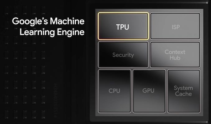
By now, it’s been quite clear that the big central talking point of the Google Tensor has been its TPU – or its Tensor Processing Unit. The TPU is, as its name implies, a custom Google developed-IP block that the company has been working on for a few years now. Until now, Google just called it the TPU inside the Tensor SoC, but at the driver level the company calls the block their “edgeTPU”. This is quite interesting as signals that the block is related to the ASIC “Edge TPU” that Google had announced back in 2018. The discrete chip had been advertised at 4 TOPs of processing power in 2 Watts of power, and while Google doesn’t advertise any performance metrics on the TPU inside the Tensor, there are entries showcasing the block goes up to 5W of power. So if the two are indeed related, then given the significant process node advantages and overall much newer IP, the performance figures of the Tensor TPU (sic) should be extremely significant.
The block is very much the pride of Google’s silicon team, telling us that it’s using the latest architecture for ML processing that’s been optimized for the way Google’s R&D teams run machine learning within the company, and promises to allow for opening up the kind of new and unique use-cases that were the main goal for making a custom SoC in the first place. We’ll go into the product-side use-cases in a more Pixel focused review later on, but the performance metrics of the TPU do appear to be impressive.
The TPU block also seems to come with some sort of block that Google calls “GSA”. This is just speculation on my part here based on the drivers, but this seems to be some sort of control block that is in charge of operating the TPU firmware, and I think contains a quad-core Cortex-A32 CPU setup.
Media Encoders, Other Stuff
On the media encoder side, the Tensor SoC uses both Samsung’s own Multi-Function Codec IP block (which is identical to what’s used on the Exynos series) as well as what appears to be a Google IP block that is dedicated to AV1 decoding. Now this is a bit weird, as Samsung does advertise the Exynos 2100 as having AV1 decode abilities, and that functionality does seem to be there in the kernel drivers. However on the Galaxy S21 series this functionality was never implemented on the Android framework level. I have no good explanation here as to why – maybe the IP isn’t working correctly with AV1.
The Google IP block, which the company calls “BigOcean”, is a dedicated AV1 decoder, and this does actually expose AV1 decoding ability to the Android framework. The very weird thing here is that all it does is AV1 – every other encoding and decoding of other formats is left over to the Samsung MFC. It’s an interesting situation and I’m left to wonder where things evolve in the next-gen SoC.
Other differences for the Tensor SoC are for example the audio subsystem. Samsung’s SoC low-power audio decoding subsystem is thrown out in favor of Google’s own block design, I didn’t dwell too much into it but generally both blocks have the same task of allowing low-power audio playback without needing to wake up large parts of the SoC. I think this block (or the GSA) is also responsible as the always-on context-hub for sensor data aggregation, with the Tensor here using Google’s IP and way of doing things versus the Exynos variant of the same block.
Google also employs a fixed function hardware memory compressor in the form of a block called Emerald Hill, which provides LZ77 compression acceleration for memory pages, and can in turn be used to accelerate ZRAM offloading in swap. I’m not sure if the Pixels are currently running this out of the box, but should be able to be confirmed by seeing “lz77eh” in /sys/block/zram0/comp_algorithm , if somebody is able to read that out. As an anecdote, as far back as 5 years ago Samsung integrated similar hardware compression IP blocks into their SoCs for the very same task, but for some reason those were never enabled for shipping devices. Maybe the energy efficiency didn’t pan out as they thought it would.
External Exynos Modem - First non-Qualcomm mmWave Phones?
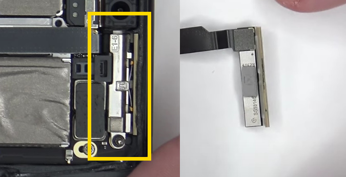
Since it’s a phone SoC, naturally the Tensor needs some sort of cellular connectivity. This is another area where Google is relying on Samsung, using the company’s Exynos Modem 5123. But, unlike the Exynos 2100 and its integrated modem, the Tensor uses a discrete external variant. As to why it’s discrete, it’s likely that with the massive GPU, larger CPU setup (two X1’s with full 1MB L2’s), and unknown size of the TPU, that the Tensor chip is quite large even in relation to the Exynos 2100.
Source: PBKreviews
Another theory on my side is that Google would somehow still be tied to Qualcomm for US networks – either for CDMA or mmWave 5G connectivity. Surprisingly, it seems this isn’t the case, as the Pixel 6 series ships with the Exynos modem across the globe. That makes the Pixel 6 family particularly interesting, as it seems that this is the first non-Qualcomm mmWave implementation out there. For reference, Samsung had talked about their mmWave RFICs and antenna modules back in 2019, saying there were plans for 2020 devices. Whether that meant designs starting in 2020 (which the Pixel 6 series would be) or commercial availability wasn’t clear at the time, but it seems that these are the first commercial phones with the solution. I don’t expect to have mmWave coverage here for myself for another few years, but third-party reports showcase the phone reaching up to 3200Mbps while other field-tests showing around half of the practical speeds of Qualcomm devices. I hope more people in the next weeks and months will have the opportunity to dive deeper into the modem’s performance characteristics.
Semi-Custom Seems Apt
Overall, the Google Tensor ends up being almost exactly what we expected the chip to be, from the earliest reports of a collaboration between Google and Samsung. Is it a Google chip? Yes, they designed it in the sense that they defined it, while also creating quite a few Google-unique blocks that are integral to the chip's differentiation. Is it a Samsung Exynos chip? Also yes, from a more foundational SoC architecture level, the Tensor has a great deal in common with Samsung’s Exynos designs. In several areas of the Tensor there are architectural and behavioral elements that are unique to Samsung designs, and aren’t found anywhere else. To that end, calling the Google Tensor a semi-custom design seems perfectly apt for what it is. That being, said, let’s see how the Tensor behaves – and where it lands in terms of performance and efficiency.
Memory Subsystem & Latency
Usually, the first concern of a SoC design, is that it requires that it performs well in terms of its data fabric and properly giving its IP blocks access to the caches and DRAM of the system within good latency metrics, as latency, especially on the CPU side, is directly proportional to the end-result performance under many workloads.
The Google Tensor, is both similar, but different to the Exynos chips in this regard. Google does however fundamentally change how the internal fabric of the chip is set up in terms of various buses and interconnects, so we do expect some differences.
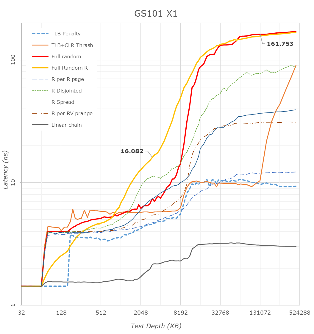
First off, we have to mention that many of the latency patterns here are still quite a broken due to the new Arm temporal prefetchers that were introduced with the Cortex-X1 and A78 series CPUs – please just pay attention to the orange “Full Random RT” curve which bypasses these.
There’s a couple of things to see here, let’s start at the CPU side, where we see the X1 cores of the Tensor chip being configured with 1MB of L2, which comes in contrast with the smaller 512KB of the Exynos 2100, but in line with what we see on the Snapdragon 888.
The second thing to note, is that it looks like the Tensor’s DRAM latency isn’t good, and showcases a considerable regression compared to the Exynos 2100, which in turn was quite worse off than the Snapdragon 888. While the measurements are correct in what they’re measuring, the problem is a bit more complex in the way that Google is operating the memory controllers on the Google Tensor. For the CPUs, Google is tying the MCs and DRAM speed based on performance counters of the CPUs and the actual workload IPC as well as memory stall % of the cores, which is different to the way Samsung runs things which are more transactional utilisation rate of the memory controllers. I’m not sure of the high memory latency figures of the CPUs are caused by this, or rather by simply having a higher latency fabric within the SoC as I wasn’t able to confirm the runtime operational frequencies of the memory during the tests on this unrooted device. However, it’s a topic which we’ll see brought up a few more times in the next few pages, especially on the CPU performance evaluation of things.
The Cortex-A76 view of things looks more normal in terms of latencies as things don’t get impacted by the temporal prefetchers, still, the latencies here are significantly higher than on competitor SoCs, on all patterns.
What I found weird, was that the L3 latencies of the Tensor SoC also look to be quite high, above that of the Exynos 2100 and Snapdragon 888 by quite a noticeable margin. I noted that one weird thing about the Tensor SoC, is that Google didn’t give the DSU and the L3 cache of the CPU cluster a dedicated clock plane, rather tying it to the frequency of the Cortex-A55 cores. The odd thing here is that, even if the X1 or A76 cores are under full load, the A55 cores as well as the L3 are still running at lower frequencies. The same scenario on the Exynos or Snapdragon chip would raise the frequency of the L3. This behaviour and aspect of the chip can be confirmed by running at dummy load on the Cortex-A55 cores in order to drive the L3 higher, which improves the figures on both the X1 and A76 cores.
The system level cache is visible in the latency hump starting at around 11-13MB (1MB L2 + 4MB L3 + 8MB SLC). I’m not showing it in the graphs here, but memory bandwidth on normal accesses on the Google chip is also slower than on the Exynos, but I think I do see more fabric bandwidth when doing things such as modifying individual cache lines – one of the reasons I think the SLC architecture is different than what’s on the Exynos 2100.
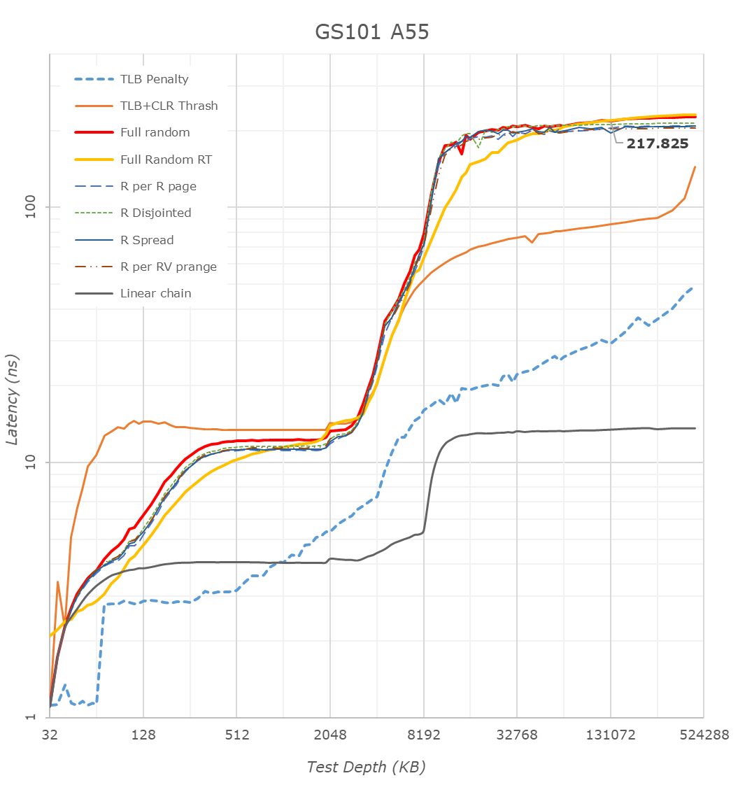
The A55 cores on the Google Tensor have 128KB of L2 cache. What’s interesting here is that because the L3 is on the same clock plane as the Cortex-A55 cores, and it runs at the same higher frequencies, is that the Tensor’s A55s have the lowest L3 latencies of the all the SoCs, as they do without an asynchronous clock bridge between the blocks. Like on the Exynos, there’s some sort of increase at 2MB, something we don’t see on the Snapdragon 888, and I think is related to how the L3 is implemented on the chips.
Overall, the Tensor SoC is quite different here in how it’s operated, and there’s some key behaviours that we’ll have to keep in mind for the performance evaluation part.
CPU Performance & Power
On the CPU side of things, the Tensor SoC, as we discussed, does have some larger configuration differences to what we’ve seen on the Exynos 2100, and is actually more similar to the Snapdragon 888 in that regard, at least from the view of a single Cortex-X1 cores. Having double the L2 cache, however being clocked 3.7%, or 110MHz lower, the Tensor and the Exynos should perform somewhat similarly, but dependent on the workload. The Snapdragon 888 showcases much better memory latency, so let’s also see if that actually plays out as such in the workloads.
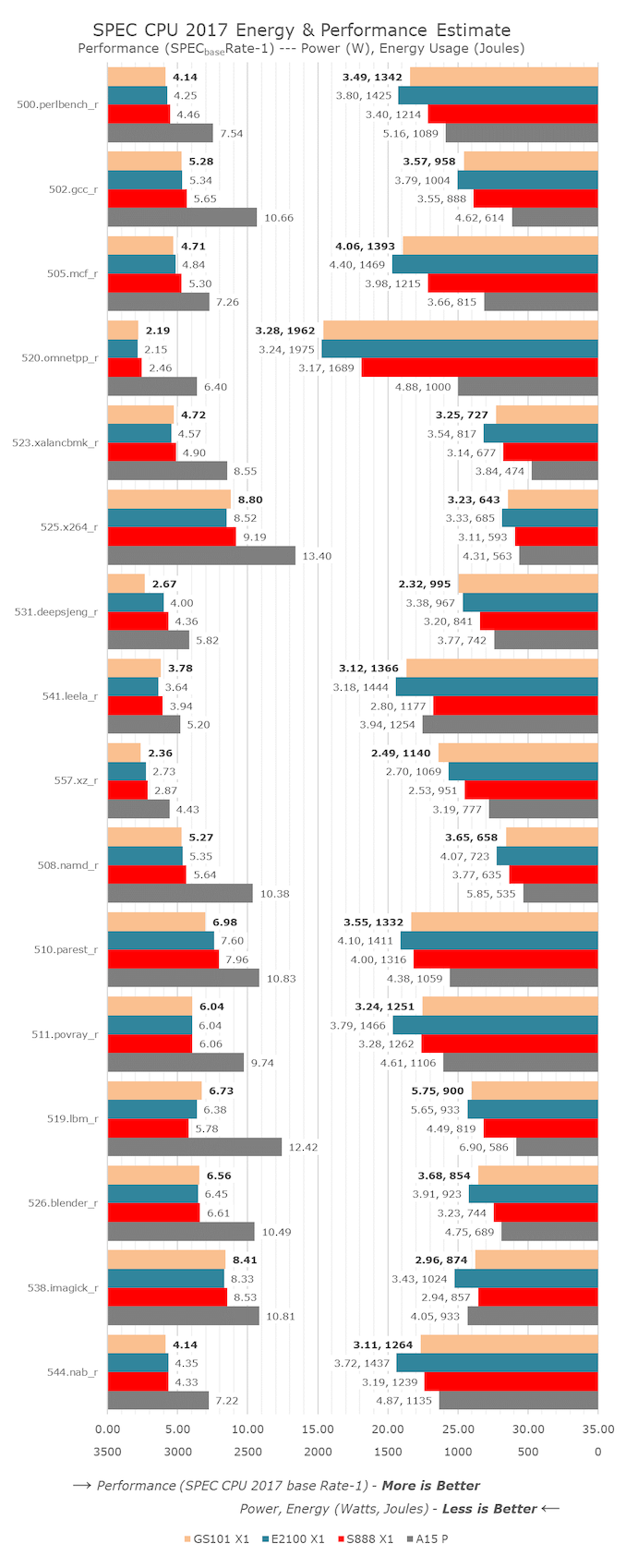
In the individual subtests in the SPEC suite, the Tensor fares well and at first glance isn’t all too different from the other two competitor SoCs, albeit there are changes, and there are some oddities in the performance metrics.
Pure memory latency workloads as expected seem to be a weakness of the chip (within what one call weakness given the small differences between the different chips). 505.mcf_r falls behind the Exynos 2100 by a small amount, the doubled L2 cache should have made more of a difference here in my expectations, also 502.gcc_r should have seen larger benefits but they fail to materialise. 519.lbm_r is bandwidth hungry and here it seems the chip does have a slight advantage, but power is still extremely high and pretty much in line with the Exynos 2100, quite higher than the Snapdragon 888.
531.deepsjeng is extremely low – I’ve seen this behaviour in another SoC, the Dimensity 1200 inside the Xiaomi 11T, and this was due to the memory controllers and DRAM running slower than intended. I think we’re seeing the same characteristic here with the Tensor as its way of controlling the memory controller frequency via CPU memory stall counters doesn’t seem to be working well in this workload. 557.xz_r is also below expectations, being 18% slower than the Snapdragon 888, and ending up using also more energy than both Exynos and Snapdragon. I remember ex-Arm’s Mike Filippo once saying that every single clock cycle the core is wasting on waiting on memory has bad effects on performance and efficiency and it seems that’s what’s happening here with the Tensor and the way it controls memory.
In more execution bound workloads, in the int suite the Tensor does well in 525.x264 which I think is due to the larger L2. On the FP suite, we’re seeing some weird results, especially on the power side. 511.povray appears to be using a non-significant amount lesser power than the Exynos 2100 even though performance is identical. 538.imagick also shows much less power usage on the part of the Tensor, at similar performance. Povray might benefit from the larger L2 and lower operating frequency (less voltage, more efficiency), but I can’t really explain the imagick result – in general the Tensor SoC uses quite less power in all the FP workloads compared to the Exynos, while this difference isn’t as great in the INT workloads. Possibly the X1 cores have some better physical implementation on the Tensor chip which reduces the FP power.
In the aggregate scores, the Tensor / GS101 lands slightly worse in performance than the Exynos 2100, and lags behind the Snapdragon 888 by a more notable 12.2% margin, all whilst consuming 13.8% more energy due to completing the task slower. The performance deficit against the Snapdragon should really only be 1.4% - or a 40MHz difference, so I’m attributing the loss here just to the way Google runs their memory, or maybe also to possible real latency disadvantages of the SoC fabric. In SPECfp, which is more memory bandwidth sensitive (at least in the full suite, less so in our C/C++ subset), the Tensor SoC roughly matches the Snapdragon and Exynos in performance, while power and efficiency is closer to the Snapdragon, using 11.5% less power than the Exynos, and thus being more efficient here.
One issue that I encountered with the Tensor, that marks it being extremely similar in behaviour to the Exynos 2100, is throttling on the X1 cores. Notably, the Exynos chip had issues running its cores at their peak freq in active cooling under room temperature (~23°C) – the Snapdragon 888 had no such issues. I’m seeing similar behaviour on the Google Tensor’s X1 cores, albeit not as severe. The phone notably required sub-ambient cooling (I tested at 11°C) to get sustained peak frequencies, scoring 5-9% better, particularly on the FP subtests.
I’m skipping over the detailed A76 and A55 subscores of the Tensor as it’s not that interesting, however the aggregate scores are something we must discuss. As alluded to in the introduction, Google’s choice of using an A76 in the chip seemed extremely hard to justify, and the practical results we’re seeing the testing pretty much confirm our bad expectations of this CPU. The Tensor is running the A76 at 2.25GHz. The most similar data-point in the chart is the 2.5GHz A76 cores of the Exynos 990 – we have to remember this was an 7LPP SoC while the Tensor is a 5LPE design like the Eynos 2100 and Snapdraogn 888.
The Tensor’s A76 ends up more efficient than the Exynos 990’s – would would hope this to be the case, however when looking at the Snapdragon 888’s A78 cores which perform a whopping 46% better while using less energy to do so, it makes the Tensor’s A76 mid-cores look extremely bad. The IPC difference between the two chips is indeed around 34%, which is in line with the microarchitectural gap between the A76 and A78. The Tensor’s cores use a little bit less absolute power, but if this was Google top priority, they could have simply clocked a hypothetical A78 lower as well, and still ended up with a more performant and more efficient CPU setup. All in all, we didn’t understand why Google chose A76’s, as all the results end up expectedly bad, with the only explanation simply being that maybe Google just didn’t have a choice here, and just took whatever Samsung could implement.
On the side of the Cortex-A55 cores, things also aren’t looking fantastic for the Tensor SoC. The cores do end up performing the equally clocked A55’s of the Snapdragon 888 by 11% - maybe due to the faster L3 access, or access to the chip’s SLC, however efficiency here just isn’t good, as it uses almost double the power, and is more characteristic of the higher power levels of the Exynos chips’ A55 cores. It’s here where I come back to say that what makes a SoC from one vendor different to the SoC from another is the very foundations and fabric design - for the low-power A55 cores of the Tensor, the architecture of the SoC encounters the same issues of being overshadowed in system power, same as we see on Exynos chips, ending up in power efficiency that’s actually quite worse than the same chips own A76 cores, and much worse than the Snapdragon 888. MediaTek’s Dimensity 1200 even goes further in operating their chip in seemingly the most efficient way for their A55 cores, not to mention Apple’s SoCs.
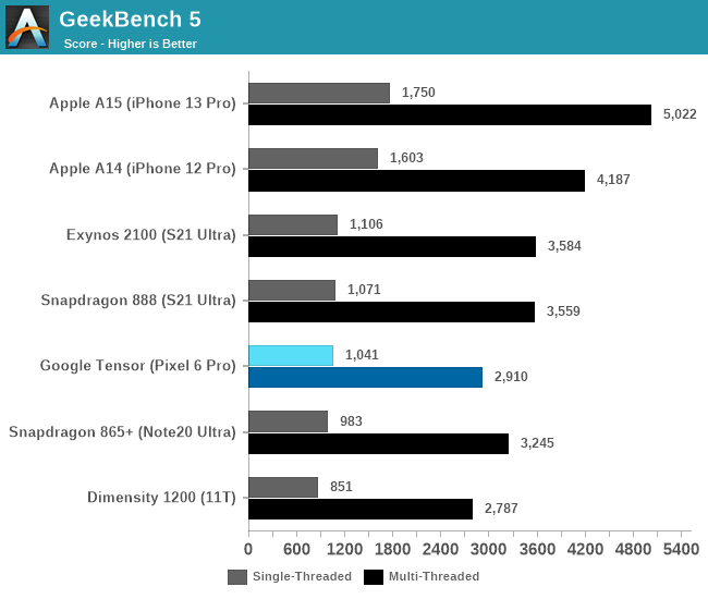
While we don’t run multi-threaded SPEC on phones, we can revert back to GeekBench 5 which serves the purpose very well.
Although the Google Tensor has double as many X1 cores as the other Android SoCs, the fact that the Cortex-A76 cores underperform by such a larger degree the middle cores of the competition, means that the total sum of MT performance of the chip is lesser than that of the competition.
Overall, the Google Tensor’s CPU setup, performance, and efficiency is a mixed bag. The two X1 cores of the chip end up slightly slower than the competition, and efficiency is most of the time in line with the Exynos 2100’s X1 cores – sometimes keeping up with the Snapdragon 888 in some workloads. The Cortex-A76 middle cores of the chip in my view make no sense, as their performance and energy efficiency just aren’t up to date with 2021 designs. Finally, the A55 behavioural characteristic showcases that this chip is very much related to Samsung’s Exynos SoCs, falling behind in efficiency compared to how Qualcomm or MediaTek are able to operate their SoCs.
GPU Performance & Power
The Google Tensors GPU is quite a beast. A Mali G78 with 20 cores, it’s sporting 42% more cores than the Exynos 2100 implementation, and only comes second after HiSilicon’s Kirin 9000. However, unlike the more power efficient N5 process node of the Kirin 9000, the Tensor SoC comes on the same process node as on the Exynos 2100. Having a much larger GPU, one would expect Google to drive the block at lower frequencies, in order to achieve better energy efficiency. To our surprise, the G78MP20 runs at up to 1GHz on the tiler and L2, and up to 848MHz on the shader cores, which is essentially the same as the smaller Exynos 2100 implementation of the GPU. Of course this immediately raises red flags for the Tensor when it comes to power consumption, as the chip certainly can’t pull out a rabbit out of a hat in terms of efficiency, so let’s see what happens:
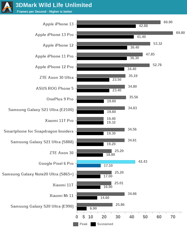
In 3DMark Wild Life unlimited, the first thing to note is that for some reason the regular Pixel 6 didn’t want to run the test as it errored out due to memory – I’m not sure what happened here, but it was isolated to the baseline model as the Pro unit had no issues.
The Pixel 6 Pro’s peak performance is respectable, however it’s only 21% faster than the Exynos 2100, not exactly what we’d expect from 21% more cores. A large issue with Mali GPUs of late has been that while you can throw more shader cores at the issue, the shared resources such as the tiler and L2 still remain as a single unit on the GPU. The G78’s ability to clock this part of the GPU higher is taken advantage of by Google in the Tensor implementation of the GPU, however that’s only 16% faster in pure clock frequency – maybe the workload is bottlenecked somewhere in this part of the GPU architecture.
Sustained performance off the start doesn’t look too good for the Pixel 6 Pro as it throttles considerably once the device gets hot, more on this in a bit.
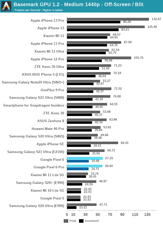
In Basemark GPU, the Pixel 6 phones both showcase odd peak performance figures that are way lower than we expected, here the chip doesn’t even manage to outperform the Exynos 2100. I’m not sure what the technical explanation here is, as on paper, the chip should be faster.
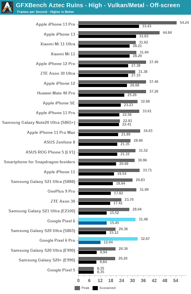
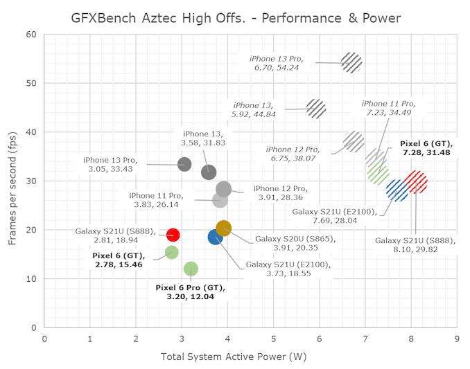
In Aztec High, the peak performance of the Tensor is again below what you’d expect, at +14% vs the Exynos 2100, and slightly ahead of the Snapdragon 888.
Sustained performance is quite bad here, and especially the Pixel 6 Pro seems to be running more severe throttling than the Pixel 6.
Looking at the power consumption of the phones, at peak performance, the Pixel 6 lands in around 7.28W, however this figure is a bit misleading. In actuality, the phone is running peak power figures in excess of 9-10W, but this is so much power, that the SoC isn’t able to complete a single run of the benchmark without throttling, so average power for a given run is actually much lower. This would also explain as to why our peak performance figures are less than what’s expected of a GPU clocked this high, it simply can’t maintain that speed for long enough to give off an FPS figure at the peak frequencies.
At sustained frequencies, the Pixel 6 and Pixel 6 Pro end up with different spots, however both are at quite low power figures around 3W.
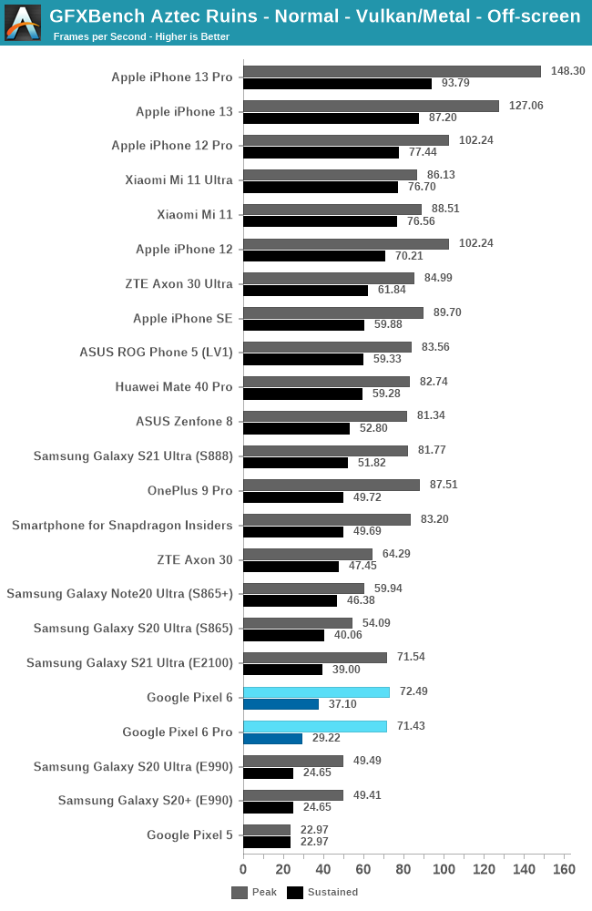
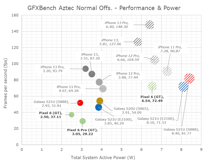
Aztec normal shows similar results, peak performance of the GPU is barely any better than the smaller configuration Exynos 2100 unit, and sustained performance figures are also significantly lower.
Sustained power after throttling on the phones is also quite weird here, as the phone seemingly throttles to <3W on the SoC. The Pixel 6 for some reason appears to have better power characteristics, it’s possible that chip bin has lower power than my 6 Pro unit.
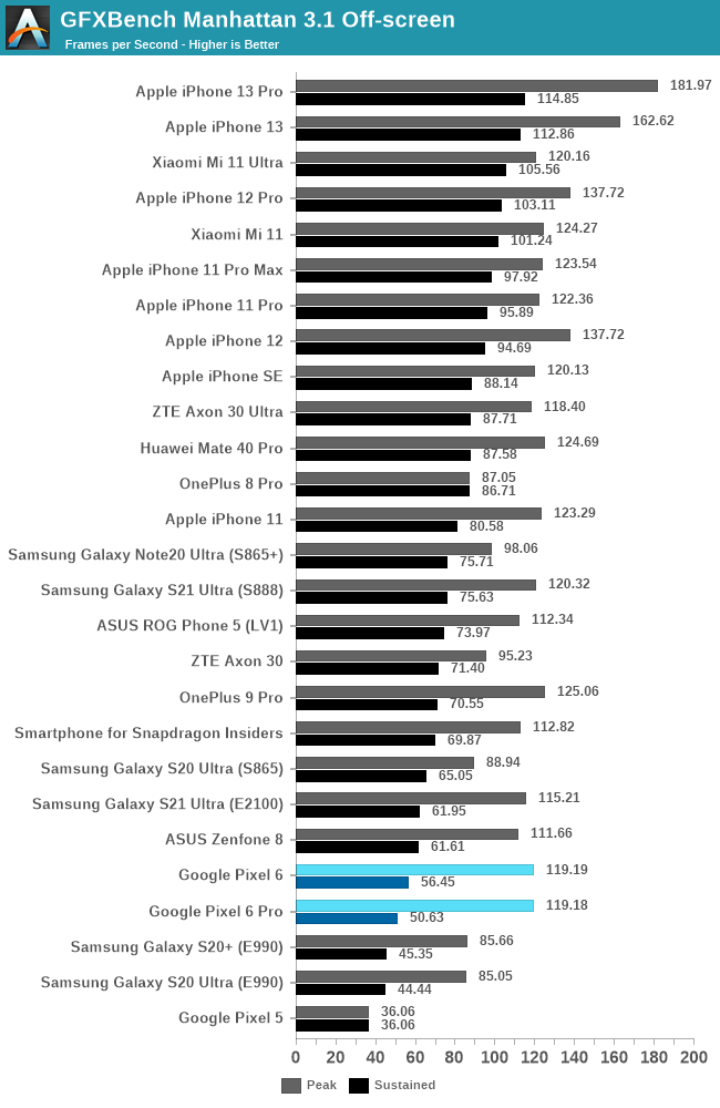
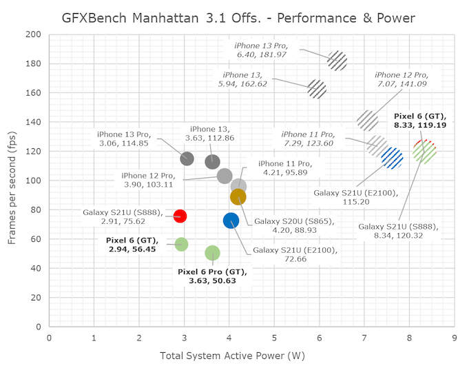
Manhattan 3.1 shows a similar peak and sustained performance standing, which isn’t too favourable for the Tensor.
Power levels in Manhattan are higher than the Aztec benchmarks, I think the CPUs, or the DRAM contribute to more of the power due to the higher achieved framerates, and it slightly helps the heat dissipation rather than having everything focused on the GPU.
Overall, the GPU performance of the Google Tensor is quite disappointing. On paper, the massive G78MP20 GPU seemed like a juggernaut at the frequencies Google delivers the chip in, but in practice, it doesn’t reach the theoretical levels of performance. That being said, over the last year of SoC releases, almost every vendor in the industry has introduced some absurd ultra-high-power GPU configuration that throttles quickly. Why they do this, I don’t know, GPU compute for burst performance is always one of the reasons given, so maybe Google is also aiming the GPU towards compute rather than gaming.
In terms of sustained performance levels, the larger GPU in theory should have allowed it to run at lower frequencies, thus at better efficiency, and in turn deliver more performance than a smaller implementation like that of the Exynos 2100. The reality here is that the Pixel 6 phones struggle with thermal dissipation, and it’s something that seems to be completely unrelated to the chip itself.
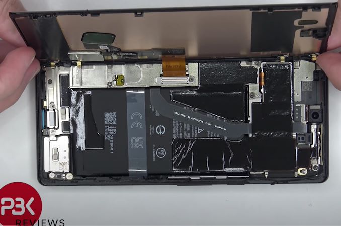
Source: PBKreviews
Both the Pixel 6 and Pixel 6 Pro are quite special in their hardware designs, in that they’re one of the rare Android devices out there which adopt an internal hardware design which doesn’t have a midframe adhered to the display panel. Looking at various teardowns of the phone, we can see that the display is relatively easily removable from the rest of the phone body, a design that’s actually more similar to Apple’s iPhones than any other Android flagship. This bodes well for the repairability of the screen, but it doesn’t do well for the thermal dissipation of the SoC. Much like iPhones have issues with thermal dissipation, and having much lower sustained power levels under stress, the Pixel 6 phones also suffer from the same issue as they cannot effectively use the display panel as a heat sink. This comes in contrast with other flagship Android devices – the Galaxy S21 Ultra for example has its display panel adhered to the midframe of the phone, it's not great for repairability, but it allows Samsung to employ a gigantic thermal dissipation pad the size of half of the phone footprint, with a direct heat pathway from the SoC to the display. Other thermally optimised devices out there share similar designs, able to better dump heat onto the full body of the phone.
The Pixel 6 Pro in contrast, has quite stark heat spots, with the left side of the phone, near the SoC, getting quite hot at up to 45°C, but at the same time the right side of the device here barely reaches 30-33°C, which is a large temperature gradient and signifies bad heat transfer abilities. Also, while I’m not sure how other people feel about this, but it does make the Pixel 6 phones feel more “hollow” in their build quality, but that might just be a nit-pick.
In any case, the Google Tensor’s chip gaming performance might be adequate, it’s no better than the Exynos 2100, and it gets further handicapped by the thermal design of the Pixel 6 phones. Generally, one can say it’s not the best phone for high-end gaming, which lines up with the subjective experiences with the devices in actual gaming demanding games like Genshin Impact.
Google's IP: Tensor TPU/NPU
At the heart of the Google Tensor, we find the TPU which actually gives the chip is marketing name. Developed by Google with input and feedback by the team’s research teams, taking advantage of years of extensive experience in the field of machine learning, Google puts a lot of value into the experiences that the new TPU allows for Pixel 6 phones. There’s a lot to talk about here, but let’s first try to break down some numbers, to try to see where the performance of the Tensor ends up relative to the competition.
We start off with MLCommon’s MLPerf – the benchmark suite works closely with all industry vendors in designing something that is representative of actual workloads that run on devices. We also run variants of the benchmark which are able to take advantage of various vendors SDKs and acceleration frameworks. Google had sent us a variant of the MLPerf app to test the Pixel 6 phones with – it’s to be noted that the workloads on the Tensor run via NNAPI, while other phones are optimised to run through the respective chip vendor’s libraries, such as Qualcomm’s SNPE, Samsung’s EDEN, or MediaTek’s Neuron – unfortunately only the Apple variant is lacking CoreML acceleration, thus we should expect lower scores on the A15.
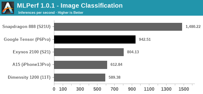
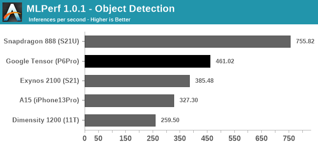
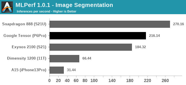
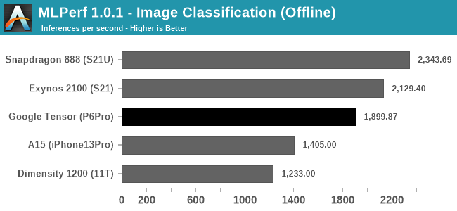
Starting off with the Image Classification, Object Detection, and Image Segmentation workloads, the Pixel 6 Pro and the Google Tensor showcase good performance, and the phone is able to outperform the Exynos 2100’s NPU and software stack. More recently, Qualcomm had optimised its software implementation for MLPerf 1.1, able to achieve higher scores than a few months ago, and this allows the Snapdragon 888 to achieve significantly better scores than what we’re seeing on the Google Tensor and the TPU – at least for those workloads, in the current software releases and optimisations.
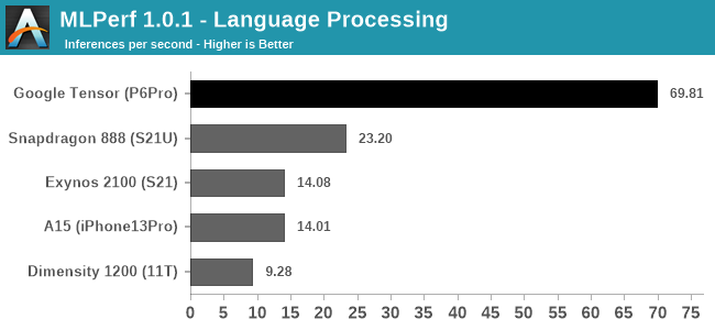
The Language Processing test of MLPerf is a MobileBERT model, and here for either architectural reasons of the TPU, or just a vastly superior software implementation, the Google Tensor is able to obliterate the competition in terms of inference speed.
In Google’s marketing, language processing, such as live transcribing, and live translations, are very major parts of the differentiating features that the new Google Tensor enables for the Pixel 6 series devices – in fact, when talking about the TPU performance, it’s exactly these workloads that the company highlights as being the killer use-cases and what the company calls state-of-the-art.
If the scores here are indeed a direct representation of Google’s design focus of the TPU, then that’s a massively impressive competitive advantage over other platforms, as it represents a giant leap in performance.
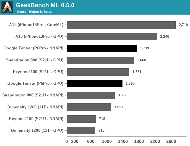
Other benchmarks we have available are for example GeekBench ML, which is currently still in a pre-release state in that the models and acceleration can still change in further updates.
The performance here depends on the APIs used, with the test either allowing TensorFlow delegates for the GPU or CPU, or using NNAPI on Android devices (and CoreML on iOS). The GPU results should only represent the GPU ML performance, which is surprisingly not that great on the Tensor, as it somehow lands below the Exynos 2100’s GPU.
In NNAPI mode, the Tensor is able to more clearly distinguish itself from the other SoCs, showcasing a 44% lead over the Snapdragon 888. It’s likely this represent the TPU performance lead, however it’s very hard to come to conclusions when it comes to such abstractions layer APIs.
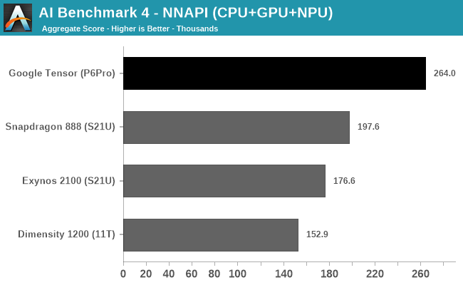
In AI Benchmark 4, when running the benchmark in pure NNAPI mode, the Google Tensor again showcases a very large performance advantage over the competition. Again, it’s hard to come to conclusions as to what’s driving the performance here as there’s use of CPU, GPU, and NPUs.
I briefly looked at the power profile of the Pixel 6 Pro when running the test, and it showcased similar power figures to the Exynos 2100, which extremely high burst power figures of up to 14W when doing individual inferences. Due to the much higher performance the Tensor showcases, it also means it’s that much more efficient. The Snapdragon 888 peaked around 12W in the same workloads, so the efficiency gap here isn’t as large, however it’s still in favour of Google’s chip.
All in all, Google’s ML performance of the Tensor has been its main marketing point, and Google doesn’t disappoint in that regard, as the chip and the TPU seemingly are able to showcase extremely large performance advantages over the competition. While power is still very high, completing an inference faster means that energy efficiency is also much better.
I asked Google what their plans are in regards to the software side of things for the TPU – whether they’ll be releasing a public SDK for developers to tap into the TPU, or whether things will remain more NNAPI centric like how they are today on the Pixels. The company wouldn’t commit yet to any plans as it’s still very early – in generally that’s the same tone we’ve heard from other companies as even Samsung, even 2 years after the release of their first-gen NPU, doesn’t publicly make available their Eden SDK. Google notes that there is massive performance potential for the TPU and that the Pixel 6 phones are able to use them in first-party software, which enables the many ML features for the camera, and many translation features on the phone.
Phone Efficiency & Battery Life
While not directly released to the Google Tensor, I also finished running the various battery tests for the Pixel 6 and Pixel 6 Pro, and there are some remarks to be made in regards to the power efficiency of the devices, and how the new SoC ends up in relation to the competition.
As a reminder, the Pixel 6 comes with a 4614mAh battery and a 6.4” 1080p 90Hz OLED screen, while the Pixel 6 Pro features a 5003mAh battery and a 6.71” 1440p 120Hz OLED display, with variable refresh rate from 10-120Hz.
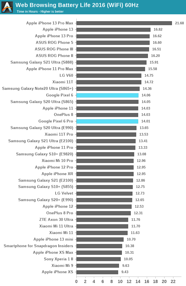
Starting off with the 60Hz web browsing results, both Pixel phones end up extremely similar in their longevity, at 14 hours runtime. The regular Pixel 6 is hard to compare things to as we don’t have too many recent phones with 90Hz displays in our results set, however the Pixel 6 Pro should be a direct comparison point to the S21 Ultras, as both feature 5000mAh batteries and similar display characteristics. The P6Pro here ends up slightly ahead of the Exynos 2100 S21 Ultra, which might not be too surprising given that the Tensor chip does end up at somewhat lower CPU power levels, even if performance is lower. It’s still quite behind the Snapdragon 888 variant of the S21 Ultra – which is again quite representative of the SoC efficiency differences.
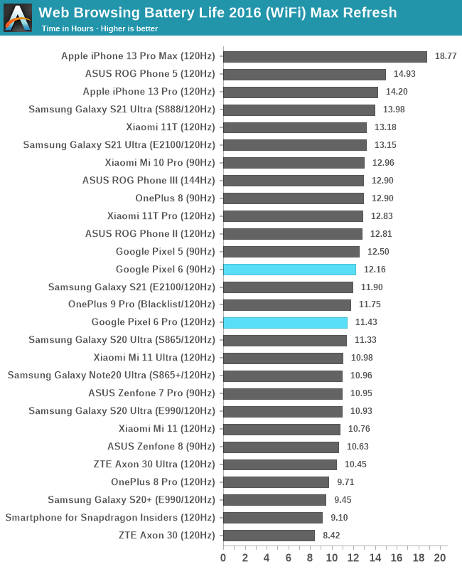
Running the phones at their respective max refresh rates, both devices see larger drops, however the Pixel 6 Pro especially sees a more substantial hit. This time around, the 6 Pro ends up significantly behind the Exynos 2100 S21 Ultra, which had only a minor drop in the 60 -> 120Hz results.
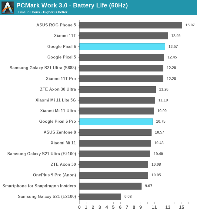
Shifting over to PCMark at 60Hz, we see that there’s a larger difference in favour of the Pixel 6, as the Pixel 6 Pro ends up behind it in longevity by almost two hours. The 6 Pro still ends up in line with the E2100 S21U, however that device showcases significantly higher performance numbers in the test, which acts both as a performance metric for device responsivity as well as a battery life test.
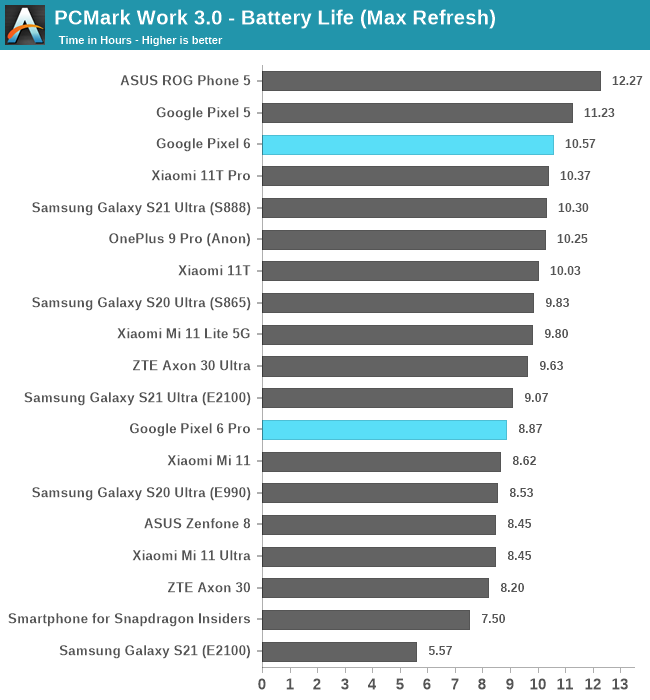
At 120Hz, the 6 Pro ends up worse than the E2100 S21U, and quite worse than the S888 S21U.
When I was investigating the phones, the 6 Pro’s power behaviour was quite weird to me, as I saw best-case baseline power figures of around 640mW, and sometimes this inexplicably would also end up at 774mW or even higher. What this reminded me of, was the power behaviour of the OnePlus 9 Pro, which also suffered from extremely high baseline power figures. Both the 6 Pro and the 9 Pro advertise themselves as having LPTO OLED panels, but both of them very clearly do not behave the same as what we’ve seen on the Note20Ultra or the S21Ultra phones. The 6 Pro also only goes up to up to 750 nits 100% APL peak brightness in auto-brightness mode under bright ambient light, which is significantly lower than the S21U’s 942 nits. I think what’s happening here is that the Pixel 6 Pro simply doesn’t have the most state-of-the-art display, and thus is quite less efficient as what we find on the competition. It does kind of make sense for the price-point of the phone, but also explains some of the battery behaviour.
Naturally, the Tensor SoC also just doesn’t appear to be as efficient. Particularly many UI workloads would be run on the A76 cores of the chip, which just outright have a 30% perf/W disadvantage. The phone ends up OK in terms of absolute battery life, however performance metrics are lower than other devices.
I think the regular Pixel 6 here is just a much better device as it doesn’t seem to have any particular issues in display efficiency, even if it’s just a 1080 90Hz panel. There are naturally experience compromises, but it’s also a $599 phone, so the value here is very good.
US readers who are used to Qualcomm phones might also encounter efficiency regressions when under cellular data – we abandoned doing testing here many years ago due to the impossible task to get consistent test environments.
Conclusion & End Remarks
Google’s newest Pixel 6 and 6 Pro are definitely most interesting devices, as in many ways they represent Google most competitive and value-rich phones the company has been able to make in years. While today’s article isn’t focusing on the device itself – more on that in a later review, including more in-depth camera coverage, what we did have a deeper look today was at the new chip powering the phones, the new Google Tensor.
The company notes that the primary reason they saw the need to go with a customized silicon approach, was that current merchant silicon solutions didn’t allow for the performance and efficiency for machine learning tasks that the company was aiming for in their devices. This performance and efficiency is used to enable new use-cases and experiences, such as the many ML features we see shipped and demonstrated in the Pixel 6 series, such live transcribing, live translation, and image processing tricks, all that run on the Tensor’s TPU.
While Google doesn’t appear to want to talk about it, the chip very clearly has provenance as a collaboration between Google and Samsung, and has a large amount of its roots in Samsung Exynos SoC architectures. While yes, it’s a customised design based on Google’s blueprints, the foundation means that some of the defining characteristics of Exynos chips is still found on the Tensor, particularly power efficiency is one area of the SoCs that are very much alike in, and that also means that the Tensor falls behind, much like the Exynos, against Qualcomm’s Snapdragon solutions when it comes to battery life or efficiency.
Google’s CPU setup is a bit different than other SoCs out there – a 2+2+4 setup with X1 cores, A76 cores and A55 cores is unusual. The two X1 cores are fine, and generally they end up where we expected them, even if there’s a few quirks. The A76 cores, ever since we heard those rumours months ago that the chip would feature them, made no sense to us, and even with the chip in our hands now, they still don’t make any sense, as they clearly fall behind the competition in both performance and efficiency. Who knows what the design process looked like, but it’s just one aspect of the chip that doesn’t work well.
GPU performance of the Tensor seems also lacklustre – while it’s hard to pinpoint wrong-doings to the actual SoC here, Google’s choice of going with a giant GPU doesn’t end up with practical advantages in gaming, as the phones themselves have quite bad thermal solutions for the chip, not able to properly dissipate the heat from the chip to the full body of the phones. Maybe Google makes more use of the GPU for burst compute workloads, but so far those were hard to identify.
So that leads us back to the core aspect of the Tensor, the TPU. It’s the one area where the SoC does shine, and very clearly has large performance, and likely also efficiency advantages over the competition. The metrics here are extremely hard to quantify, and one does pose the question if the use-cases and features the Pixel 6 comes with were really impossible to achieve, on say a Snapdragon chip. At least natural language processing seems to be Google’s and the Tensor’s forte, where it does have an inarguably large lead.
One further aspect that isn’t discussed as much is not related to the performance of the chip, but rather the supply chain side of things. We of course have no idea what Google’s deal with Samsung looks like, however both new Pixel 6 phones are devices that seemingly are priced much more aggressively than anything we’ve seen before from the company. If this is related to the SoC bill of materials is just pure speculation, but it is a possibility in my mind.
In general, I do think Google has achieved its goals with the Tensor SoC. The one thing it promises to do, it does indeed do quite well, and while the other aspects of the chip aren’t fantastic, they’re not outright deal-breakers either. I still think energy efficiency and battery life are goals of highest priority in a design, and there we just absolutely need to see better improvements in the next generation Tensor. We don’t know what path Google is taking for future designs, but it’ll be interesting to see.
We’ll be following up with a more in-depth review of the actual Pixel 6 phones, starting with a camera-focused article – stay tuned.

