Original Link: https://www.anandtech.com/show/16979/the-ampere-altra-max-review-pushing-it-to-128-cores-per-socket
The Ampere Altra Max Review: Pushing it to 128 Cores per Socket
by Andrei Frumusanu on October 7, 2021 8:00 AM EST- Posted in
- Arm
- Servers
- Neoverse N1
- Ampere
- Altra Max

It’s been a little over a year since Ampere started to deliver their first generation Altra processors. The “Quicksilver” design with 80 Neoverse N1 cores was the first merchant Arm silicon on the market who really went “all-out” in terms of performance targets, aiming for the best of what AMD and Intel had to offer, ending up in a very competitive standing against the newest EPYC CPUs and leapfrogging Intel’s offerings.
Since that first review, the competition has released two new generation platforms, the newer EPYC Milan chips, showcasing a good generational boost, and Intel dramatically narrowing the performance gap with the new Ice Lake-SP Xeon parts.
Related Reading:
-
The Ampere Altra Review: 2x 80 Cores Arm Server Performance Monster
-
AMD EPYC Milan Review Part 2: Testing 8 to 64 Cores in a Production Platform
-
AMD 3rd Gen EPYC Milan Review: A Peak vs Per Core Performance Balance
-
Intel 3rd Gen Xeon Scalable (Ice Lake SP) Review: Generationally Big, Competitively Small
For the Arm ecosystem and Ampere in particular, things naturally also aren’t standing still; following the first-gen 80-core Quicksilver design, we had long expected the 128-core “Mystique” Altra Max design. Arguably a bit late compared to Ampere’s initial Q4 2020 projections, we’ve now finally had our hands on the new many-core monster for today’s initial review.
Pushing it to 128 Cores
The new Altra Max is a quite exciting part, but it’s also relatively straightforward design compared to the original Altra parts. While the original chip had been pushing 80 Neoverse-N1 cores, the new Altra Max is pushing 128 cores. While there are also slightly improved technical differences between the two chip generations, that is mostly the main large differentiation between the two designs.
Ampere is still continuing to offer both Altra and Altra Max chips in their product line-up, with the Max parts in particular filling the high-core count SKU segment:
| Ampere Altra SKU List | ||||||
| AnandTech | Cores | Frequency | TDP | PCIe | DDR4 | Price |
| Altra Max "Mystique" | ||||||
| M128-30 (Tested) |
128 | 3.0 GHz | 250 W | 128x G4 | 8 x 3200 | $5800 |
| M128-28 | 128 | 2.8 GHz | 230 W | 128x G4 | 8 x 3200 | $5500 |
| M128-26 | 128 | 2.6 GHz | 190 W | 128x G4 | 8 x 3200 | $5400 |
| M112-30 | 112 | 3.0 GHz | 240 W | 128x G4 | 8 x 3200 | $5100 |
| M96-30 | 96 | 3.0 GHz | 220 W | 128x G4 | 8 x 3200 | $4550 |
| M96-28 | 96 | 2.8 GHz | 190 W | 128x G4 | 8 x 3200 | $4250 |
| Altra "Quicksilver" | ||||||
| Q80-33 (Tested) |
80 | 3.3 GHz | 250 W | 128x G4 | 8 x 3200 | $4050 |
| Q80-30 | 80 | 3.0 GHz | 210 W | 128x G4 | 8 x 3200 | $3950 |
| Q80-26 | 80 | 2.6 GHz | 175 W | 128x G4 | 8 x 3200 | $3810 |
| Q72-30 | 72 | 3.0 GHz | 195 W | 128x G4 | 8 x 3200 | $3590 |
| Q64-33 | 64 | 3.3 GHz | 220 W | 128x G4 | 8 x 3200 | $3810 |
| Q64-30 | 64 | 3.0 GHz | 180 W | 128x G4 | 8 x 3200 | $3480 |
| Q64-26 | 64 | 2.6 GHz | 125 W | 128x G4 | 8 x 3200 | $3260 |
| Q64-24 | 64 | 2.4 GHz | 95 W | 128x G4 | 8 x 3200 | $3090 |
| Q32-17 | 32 | 1.7 GHz | 45 W | 128x G4 | 8 x 3200 | $800 |
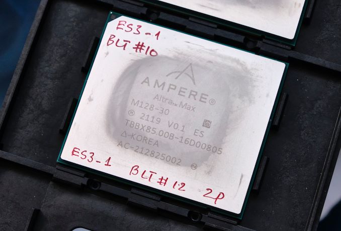
The unit we’re testing today, the flagship Altra Max M128-30, with 128 cores and a 3.0GHz clock (again, noteworthy congratulations of Ampere’s straightforward and descriptive part naming), with a maximum TDP of 250W.
Much like the first-generation parts, platform side features are all identical throughout the product stack, always featuring the maximum 128 lanes of PCIe 4.0 and 8-channel DDR4-3200 capabilities.
Comparing the M128-30 to the Q80-33, the new Altra Max part is able to fit in 60% more cores, albeit at 10% lower frequency, within the same advertised TDP. It’s to be noted that TDP here doesn’t mean power consumption, and in our initial review of the Q80-33 we noted that the chip in many workloads hovered at power levels much below the TDP, possibly explaining why and Ampere was able to grow the core count this much even though the chip isn’t on a fundamentally different process node (TSMC N7), though it’s on a better implementation.
The SKU list for the new Altra Max parts is interesting in that there’s only parts from 96 cores onwards, with anything below that still being serviced by the original Altra SKUs. It’s very likely that due to the process node maturity of the N7 node that Ampere here likely has few chips yielding with fewer cores, and the higher clocks and larger cache of the Quicksilver chips would be better served for lower core count deployments anyhow.
In terms of pricing, Ampere is quite aggressive, vastly undercutting both AMD and Intel’s flagship parts MSRPs, though as always, what large customers and hyperscalers pay are most of the time never in line with those prices anyhow – but it’s still a large win for Ampere in terms of visible pricing.
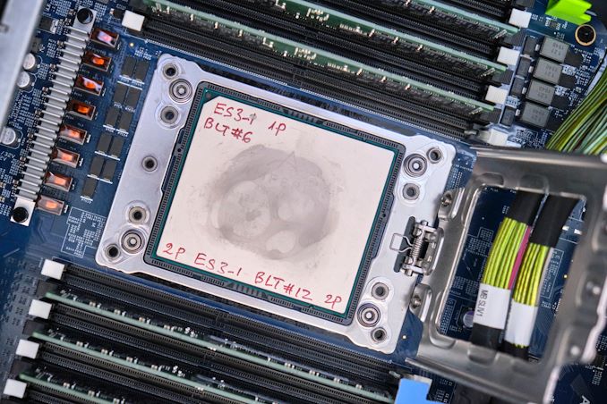
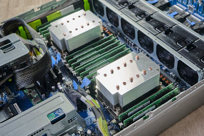
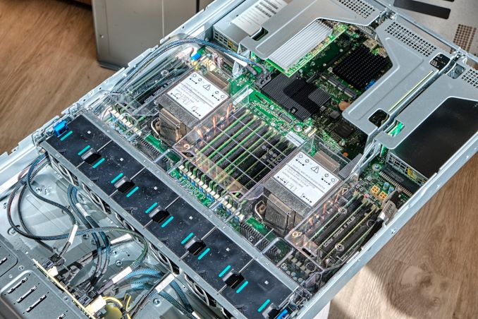
The Altra Max is extremely straightforward in terms of deployment: following some initial required firmware updates, it’s essentially a drop-in solution on the existing Altra platforms, which is exactly what we did for our review, re-using the original Mount Jade reference server from Wiwynn. The only practical note to make here is that at time of writing, Ampere currently doesn’t have a dual capable firmware stack that would enable swapping around from Altra to Altra Max and vice-versa, our initial setup was a one-way upgrade, with interoperability firmware still being something in the works for the future.
Test Bed and Setup - Compiler Options
For the rest of our performance testing, we’re disclosing the details of the various test setups:
Ampere "Mount Jade" - Dual Altra Max M128-30 / Altra Q80-33
For the Ampere system, we’re still using our Mount Jade server, manufactured by Wiwynn, featuring Ampere’s Mount Jade DVT reference motherboard, testing both the Q80-33 and the new M128-30.
In terms of memory, we’re using the bundled 16 DIMMs of 32GB of Samsung DDR4-3200 for a total of 512GB, 256GB per socket.
| CPU | 2x Ampere Altra Max M128-30 (3.0 GHz, 128c, 16MB L3, 250W) 2x Ampere Altra Q80-33 (3.3 GHz, 80c, 32 MB L3, 250W) |
| RAM | 512 GB (16x32 GB) Samsung DDR4-3200 |
| Internal Disks | Samsung MZ-QLB960NE 960GB Samsung MZ-1LB960NE 960GB |
| Motherboard | Mount Jade DVT Reference Motherboard |
| PSU | 2000W (94%) |
We’re running an Ubuntu 21.04 server image – naturally because the system is Arm SBSA compatible, you’re able to boot off any compatible generic Linux distribution off of it.
The system has all relevant security mitigations activated, including SSBS (Speculative Store Bypass Safe) against Spectre variants.
The system has all relevant security mitigations activated against the various vulnerabilities.
AMD - Dual EPYC 7763 / 75F3 / 7443 / 7343 / 72F3
Our AMD platform for the Milan generation is a GIGABYTE’s MZ72-HB0 rev.3.0 board as the primary test platform for the EPYC 7763, 75F3, 7443, 7343 and 72F3. The system is running under full default settings, meaning performance or power determinism as configured by AMD in their default SKU fuse settings.
| CPU | 2x AMD EPYC 7763 (2.45-3.500 GHz, 64c, 256 MB L3, 280W) / 2x AMD EPYC 75F3 (3.20-4.000 GHz, 32c, 256 MB L3, 280W) / 2x AMD EPYC 7443 (2.85-4.000 GHz, 24c, 128 MB L3, 200W) / 2x AMD EPYC 7343 (3.20-3.900 GHz, 16c, 128 MB L3, 190W) / 2x AMD EPYC 72F3 (3.70-4.100 GHz, 8c, 256MB L3, 180W) |
| RAM | 512 GB (16x32 GB) Micron DDR4-3200 |
| Internal Disks | Crucial MX300 1TB |
| Motherboard | GIGABYTE MZ72-HB0 (rev. 3.0) |
| PSU | EVGA 1600 T2 (1600W) |
Software wise, we ran Ubuntu 20.10 images with the latest release 5.11 Linux kernel. Performance settings both on the OS as well on the BIOS were left to default settings, including such things as a regular Schedutil based frequency governor and the CPUs running performance determinism mode at their respective default TDPs unless otherwise indicated.
AMD - Dual EPYC 7713 / 7662
A few performance figures of the EPYC Milan 7713 and Rome 7762 parts were done on AMD’s Daytona system – unfortunately we no longer have access to these SKUs so this is why the differing platform.
| CPU | 2x AMD EPYC 7713 (2.00-3.365 GHz, 64c, 256 MB L3, 225W) / 2x AMD EPYC 7662 (2.00-3.300 GHz, 64c, 256 MB L3, 225W) |
| RAM | 512 GB (16x32 GB) Micron DDR4-3200 |
| Internal Disks | Varying |
| Motherboard | Daytona reference board: S5BQ |
| PSU | PWS-1200 |
AMD - Dual EPYC 7742
Our local AMD EPYC 7742 system is running on a SuperMicro H11DSI Rev 2.0.
| CPU | 2x AMD EPYC 7742 (2.25-3.4 GHz, 64c, 256 MB L3, 225W) |
| RAM | 512 GB (16x32 GB) Micron DDR4-3200 |
| Internal Disks | Crucial MX300 1TB |
| Motherboard | SuperMicro H11DSI0 |
| PSU | EVGA 1600 T2 (1600W) |
As an operating system we’re using Ubuntu 20.10 with no further optimisations. In terms of BIOS settings we’re using complete defaults, including retaining the default 225W TDP of the EPYC 7742’s, as well as leaving further CPU configurables to auto, except of NPS settings where it’s we explicitly state the configuration in the results.
The system has all relevant security mitigations activated against speculative store bypass and Spectre variants.
Intel - Dual Xeon Platinum 8380
For our new Ice Lake test system based on the Whiskey Lake platform, we’re using Intel’s SDP (Software Development Platform 2SW3SIL4Q, featuring a 2-socket Intel server board (Coyote Pass).
The system is an airflow optimised 2U rack unit with otherwise little fanfare.
Our review setup solely includes the new Intel Xeon 8380 with 40 cores, 2.3GHz base clock, 3.0GHz all-core boost, and 3.4GHz peak single core boost. That’s unusual about this part as noted in the intro, it’s running at a default 205W TDP which is above what we’ve seen from previous generation non-specialised Intel SKUs.
| CPU | 2x Intel Xeon Platinum 8380 (2.3-3.4 GHz, 40c, 60MB L3, 270W) |
| RAM | 512 GB (16x32 GB) SK Hynix DDR4-3200 |
| Internal Disks | Intel SSD P5510 7.68TB |
| Motherboard | Intel Coyote Pass (Server System S2W3SIL4Q) |
| PSU | 2x Platinum 2100W |
The system came with several SSDs including Optane SSD P5800X’s, however we ran our test suite on the P5510 – not that we’re I/O affected in our current benchmarks anyhow.
As per Intel guidance, we’re using the latest BIOS available with the 270 release microcode update.
Intel - Dual Xeon Platinum 8280
For the older Cascade Lake Intel system we’re also using a test-bench setup with the same SSD and OS image as on the EPYC 7742 system.
Because the Xeons only have 6-channel memory, their maximum capacity is limited to 384GB of the same Micron memory, running at a default 2933MHz to remain in-spec with the processor’s capabilities.
| CPU | 2x Intel Xeon Platinum 8280 (2.7-4.0 GHz, 28c, 38.5MB L3, 205W) |
| RAM | 384 GB (12x32 GB) Micron DDR4-3200 (Running at 2933MHz) |
| Internal Disks | Crucial MX300 1TB |
| Motherboard | ASRock EP2C621D12 WS |
| PSU | EVGA 1600 T2 (1600W) |
The Xeon system was similarly run on BIOS defaults on an ASRock EP2C621D12 WS with the latest firmware available.
Compiler Setup
For compiled tests, we’re using the release version of GCC 10.2. The toolchain was compiled from scratch on both the x86 systems as well as the Altra system. We’re using shared binaries with the system’s libc libraries.
128 Cores Mesh Setup & Memory Subsystem
Starting off the testing, one thing that is extremely intriguing about Ampere’s implementation of their Altra designs is the fact that they’re achieving more than 64 cores whilst still using Arm’s CMN-600 mesh network IP. In our more recent coverage earlier this year of Arm’s newer upcoming CMN-700 mesh network, we wrote about the fundamental structure of the CMN mesh and its building blocks, such as RN-F, HN-F, and components such as CALs.
In a typical deployment, a mesh consists of cross-points (XPs) to whose RN-F (Fully coherent request node) connect to either directly a CPU, or a CAL (component aggregation layer) which can house two CPUs.
Our initial confusion last year with the Quicksilver designs was that 80 cores was more cores than what the CMN would actually support when configured with the maximum mesh size and two cores per CAL per XP – at least officially. Ampere back then was generally coy about talking about the mesh setup, but more recent discussions with Arm and Ampere, the companies have divulged that it’s also possible to house the CPUs inside of a DSU (DynamiQ Shared Unit), the same cluster design that we find in mobile Arm SoCs with Cortex CPUs.
Ampere has since confirmed the mesh setup in regards to the CPUs: instead of housing cores directly to the mesh via RN-Fs, or even via a CAL on each XP, they are employing two DSUs, each with two Neoverse-N1 cores, connected to a CAL, connected to a single XP. That means each mesh cross-point houses four cores, vastly reducing the needed mesh size to be able get to such core numbers – this is both valid for the Quicksilver 80-core designs and the new Mystique 128-core designs. The only differences with the Mystique design is that Ampere has now simply increased the mesh size (we still don’t have official confirmation on the exact setup here).
From a topology perspective, the Altra Max is still a massive monolithic 128-core chip, with competitive core-to-core latencies within the same socket. Our better understanding of the use of DSUs in the design now also explains the more unique low-latency figures of 26ns which only happens between two core pairs – these would presumably be two sibling cores housed within a single DSU, and coherency and communications between the two doesn’t have to go out into the mesh, which incurs higher latencies.
We had discussed Ampere’s quite high inter-socket latencies in our review of the Altra last year, as a fresh reminder, this is because the design doesn’t have a single coherency protocol that spans from the mesh network to the remote mesh of the other socket – instead having to have to go through an intermediary cache-coherency protocol translation for inter-socket communication, CCIX in this case. In particular this wasn’t very efficient for when two cores within a socket have to work on a remote socket cache line – the communication between cores in DSU is very efficient here, however between cores in a mesh it means doing a round-trip to the remote socket, resulting in pretty awful latencies.
The good news for the new Altra Max design is that Ampere was able to vastly improve the inter-socket communication overhead by optimising the CCIX stack part of things. The results are that socket-to-socket core latencies have gone down from ~350ns to ~240ns, and the aforementioned core-to-core within a socket with a remote cache line from ~650ns to ~450ns – still pretty bad, but undoubtedly a large improvement.
Latencies within a socket can be up at the extremes, simply due to the larger mesh. Ampere has boosted the mesh frequency from 1800MHz to 2000MHz in this generation, so there is a slight boost there as well as associated bandwidth.
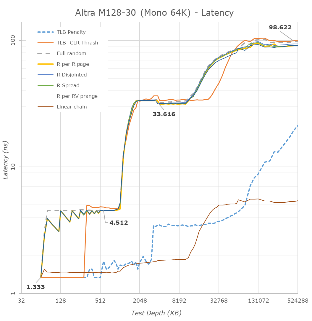
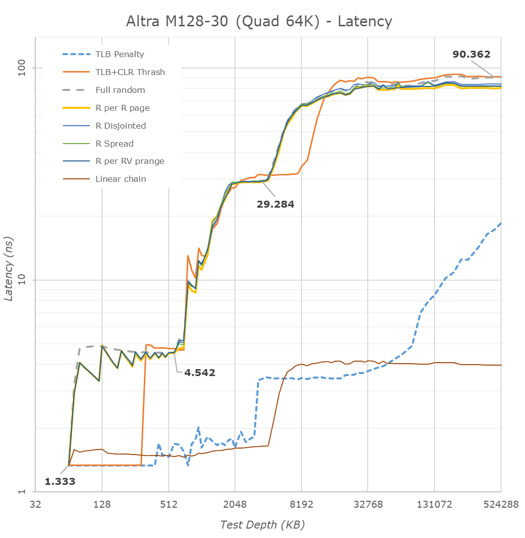
Looking at the memory latencies of the new part, comparing the Q80-33 to the M128-30 results at 64KB page size, of course the first thing that is noticeable is the fact that the new Altra Max system now only has 16MB of SLC, or system level cache, half of the 32MB of the Quicksilver design. This was one of the compromises the company decided to make when increasing the core count and mesh in the Mystique design.
L3/SLC latencies are also slightly up from 30 to 33.6ns, some of that is the 10% slower CPU clock, but most of it is because the larger mesh with more wire distance and more cross-points for data to travel across.
One thing that we hadn’t covered in our initial review was the chip running regular 4K pages – the most surprising aspect here is not the fact that things look a bit different due to the 4K pages themselves, but rather because the prefetchers now behave totally differently. In our first review we believed that Ampere had intentionally disabled the prefetchers due to the sheer core count of the system, but looking at the 4K page results here they appear to be in line with what we saw in behaviour in Amazon’s Graviton2. Notably the area/region prefetcher no longer pulls in whole pages in patterns which have strong region locality, such as the “R per R page” pattern (Random cache lines within a page followed by random pages traversal). Ampere confirmed that this was not an intentional configuration at 64KB pages, though we didn’t have an exact explanation for it. I theorise it’s maybe a microarchitectural aspect of the N1 cores trying to avoid increased cache pressure at larger page sizes.
This weird behaviour also explains the discrepancy in scores between Graviton2 and Altra in SPEC’s 507.cactuBSSN_r, which is actually due to the prefetchers working or not between 64/4KB pages.
It’s still possible to run the chip in either monolithic, hemisphere, or quadrant modes, segmenting the memory accesses between the various memory controller channels on the chip, as well as the SLC. Unfortunately, at 128 cores and only 16MB of SLC, the quadrant mode results in only 4MB of SLC, which is quite minuscule for a desktop machine, much less a server system. Each core still has 1MB of L2, however as we’ll see later in the tests, there are real-world implications of such tiny SLC sizes.
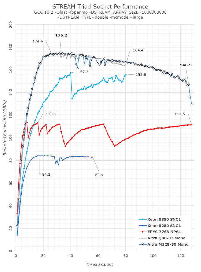
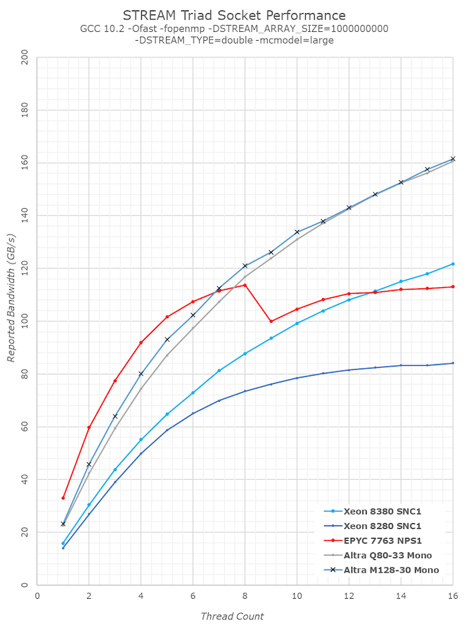
In terms of DRAM bandwidth, the Altra system on paper is equal to AMD’s EPYC Rome or Milan, or Intel’s newest Ice Lake-SP parts, due to all of them running 8-channel DDR4-3200. Ampere’s advantage comes from the fact that it is able to detect streaming memory workloads and automatically transform them into non-temporal writes, avoiding an extra memory read due to RFO (read for ownership) operations that “normal” designs have to go through. Intel’s newest Ice Lake-SP design has a somewhat similar optimisation, though working more on a cache-line basis and seemingly not able to extract as much bandwidth efficiency as the Arm design. AMD currently lacks any such optimisation and software has to have explicit usage of non-temporal writes to be able to fully extract the most out of the memory subsystem – which isn’t as optimal as a generic workload agnostic optimisation that Ampere or Intel currently employ.
Between the Q80-33 and M128-30, we’re seeing bandwidth curves that roughly match – up to a certain core count. The new M128-30 naturally goes further to 128 cores, but the resulting aggregate bandwidth also goes further down due to resource contention on the SoC – something very important to keep in mind as we explore more detailed workload results on the next pages.
At lower core count load, we’re seeing the M128-30 bandwidth exceed that of the Q80-33 even though it’s at lower CPU frequencies, again this is likely due to the fact that the mesh is now running 11% faster in frequency on the new design. AMD’s EPYC Milan still has access to the most per-core bandwidth in low thread situations.
SPEC - Multi-Threaded Performance - Subscores
We’re starting off with the multi-threaded/process SPEC CPU rate results. As usual, because there are not officially submitted scores to SPEC, we’re labelling the results as “estimates” as per the SPEC rules and license.
We compile the binaries with GCC 10.2 on their respective platforms, with simple -Ofast optimisation flags and relevant architecture and machine tuning flags (-march/-mtune=Neoverse-n1 ; -march/-mtune=skylake-avx512 ; -march/-mtune=znver2).
We’re focusing our comparisons between the new M128-30, the previous Q80-33, and AMD’s flagship EPYC 7763 and Intel’s new Xeon 8380. The Altra chips are running at 250W TDPs at respectively 128/80 cores, the EPYC at 280W and 64 cores, and the Xeon at 270W for 40 cores. The SMT systems have it enabled, and we’re running peak threads in these subscores.
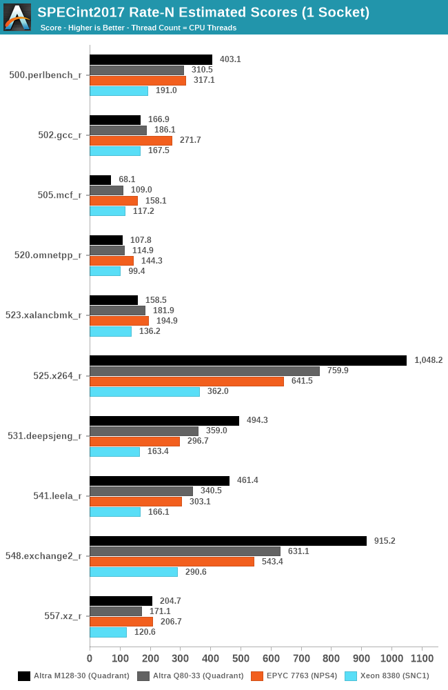
In SPECint2017, we’re seeing two different result-sets for the new Altra Max system – either very large gains, or some more notable performance regressions.
Workloads such as 525.x264_r, 531.deepsjeng_r, 541.leela_r, and 548.exchange2_r, have one large commonality about them, and that is that they’re not very memory bandwidth hungry, and are able to keep most of their working sets within the caches. For the Altra Max, this means that it’s seeing performance increases from 38% to 45% - massive upgrades compared to the already impressive Q80-33.
The 45% increase in 548.exchange2_r is essentially almost perfect linear scaling with the core count and frequencies; although the M128-30 has 60% more cores, it’s also running at 10% lower frequencies, so 45% more theoretical throughput.
523.xlancbmk_r also isn’t very DRAM traffic heavy in traditional systems, however it has a larger working set than the other aforementioned workloads, and the smaller SLC size and increased core count don’t do it favours as it becomes resource contended. The same can be said of 502.gcc_r, which is also slower than the Q80-33.
505.mcf_r is the worst-case scenario, although memory latency sensitive, it also has somewhat higher bandwidth that can saturate a system at higher instance count, and adding cores here, due to the bandwidth curve of the system, has a negative impact on performance as the memory subsystem becomes more and more inefficient. The same workload with only 32 or 64 instances scores 83.71 or 101.82 respectively, much higher than what we’re seeing with 128 cores.
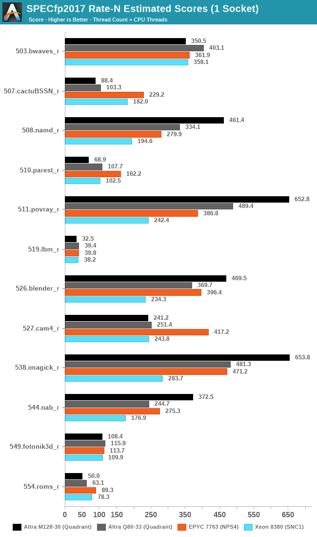
In the FP suite, we’re seeing a same differentiation between the M128-80 and the other systems. In anything that is more stressful on the memory subsystem, the new Mystique chip doesn’t do well at all, and most times regresses over the Q80-33.
In anything that’s simply execution bound, throwing in more execution power at the problem through more cores of course sees massive improvements. In many of these cases, the M128-30 can now claim a rather commanding lead over the competition Milan chip, and leaving even Intel’s new Ice Lake-SP in the dust due to the sheer core count and efficiency advantage.
SPEC - Multi-Threaded Performance - Aggregate
Switching over to the aggregate geomean scores for the suites, we see a more moderate view of the generational improvements of the Altra Max chip:
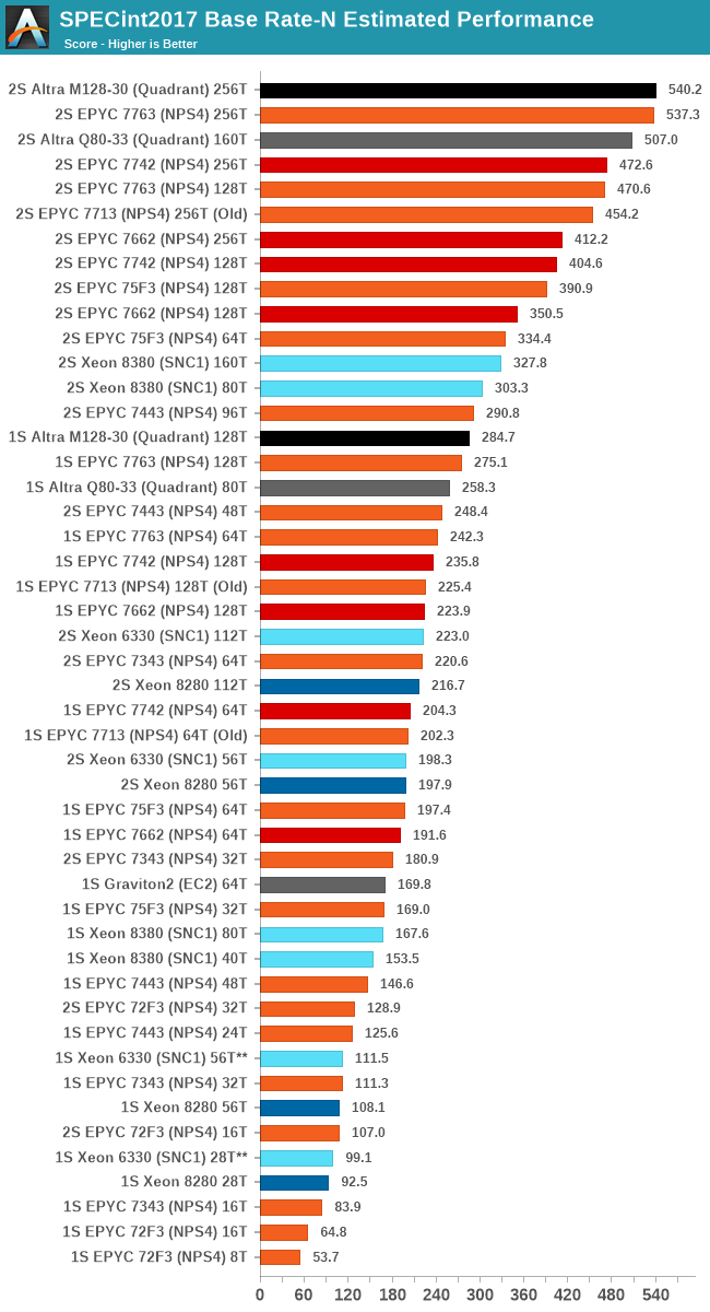
In the integer suite, the M128-30 only sees a 6-10% advantage over the Q80-33 depending on the 2- or 1-socket scores. It’s a smidge faster than the EPYC 7763, but there’s more considerations to have than just the total scores.
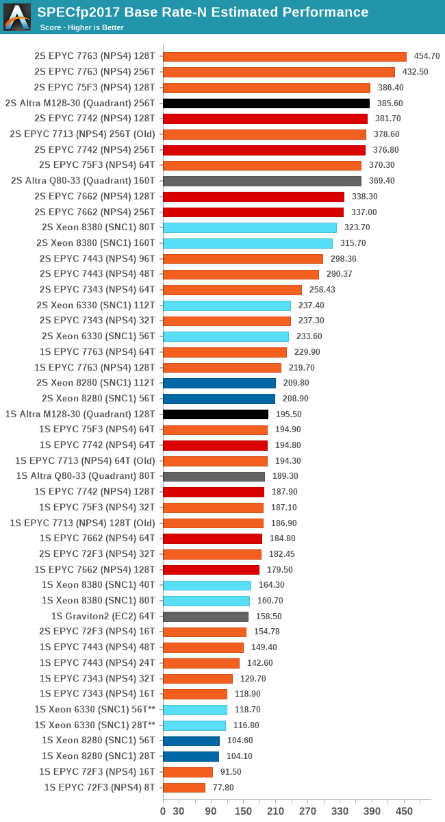
In the floating-point suite, the system also sees rather lacklustre figures of only 3-4% advantage of the M128-30 over the Q80-33.
The general problem of these scores showcase is a trend of the new Altra Max design, and that is that it’s not as general-purpose as we tend to expect for a CPU. Even though we see regular large workload gains of 30-45%, the way the suite is designed for the “base” scores is that we’re running all workloads with the same number of instances, something which at 128 cores on the Altra Max inevitably leads to performance regressions in anything that is more demanding on memory and caches.
When we first heard of the Altra Max only featuring a 16MB cache, we were quite pessimistic of this aspect of the design, well – that was also true of the 32MB cache of the 80-core Altra, where performance in some workloads just can not scale well beyond a certain core count due to the shared resource contention.
SPEC - Single-Threaded Performance
Single-threaded performance is important for some more real-world workloads, although for the Altra Max which advertises itself as a throughput machine for hyperscaler use, it’s probably only a very edge-case scenario metric.
We don’t expect much of the chip here, given it’s halved SLC size, and 10% lower frequencies compared to the Q80-33.
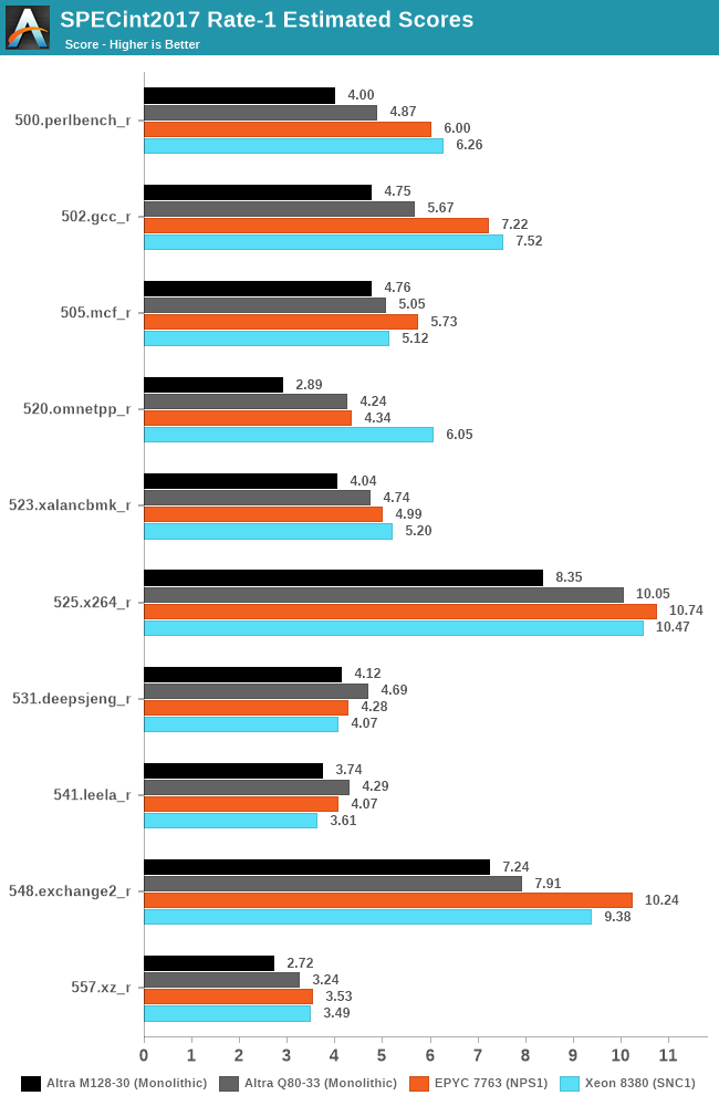

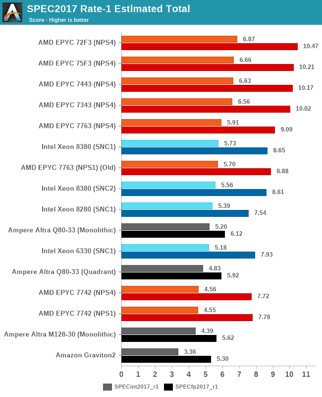
As one would think, the M128-30 doesn’t have much going for it in such a load scenario, showcasing 8-15% lower scores than the Q80-33, and falling behind most of the competitive pack, except for the 2.6GHz clocked Graviton2.
SPEC - Per-Core Performance under Load
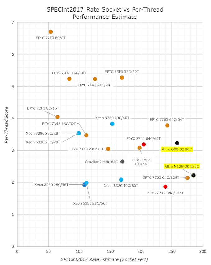
A metric that is actually more interesting than isolated single-thread performance, is actually per-thread performance in a fully loaded system. This actually is a measurement and benchmark figure that would greatly interest enterprises and customers which are running software or workloads that are possibly licensed on a per-core basis, or simply workloads that require a certain level of per-thread service level agreement in terms of performance.
The Altra Max here is inevitably expected to post worse metrics than the Altra – first of all due to the 10% lower core frequencies, and second of all due to lower shared resources that need to be shared amongst more cores.
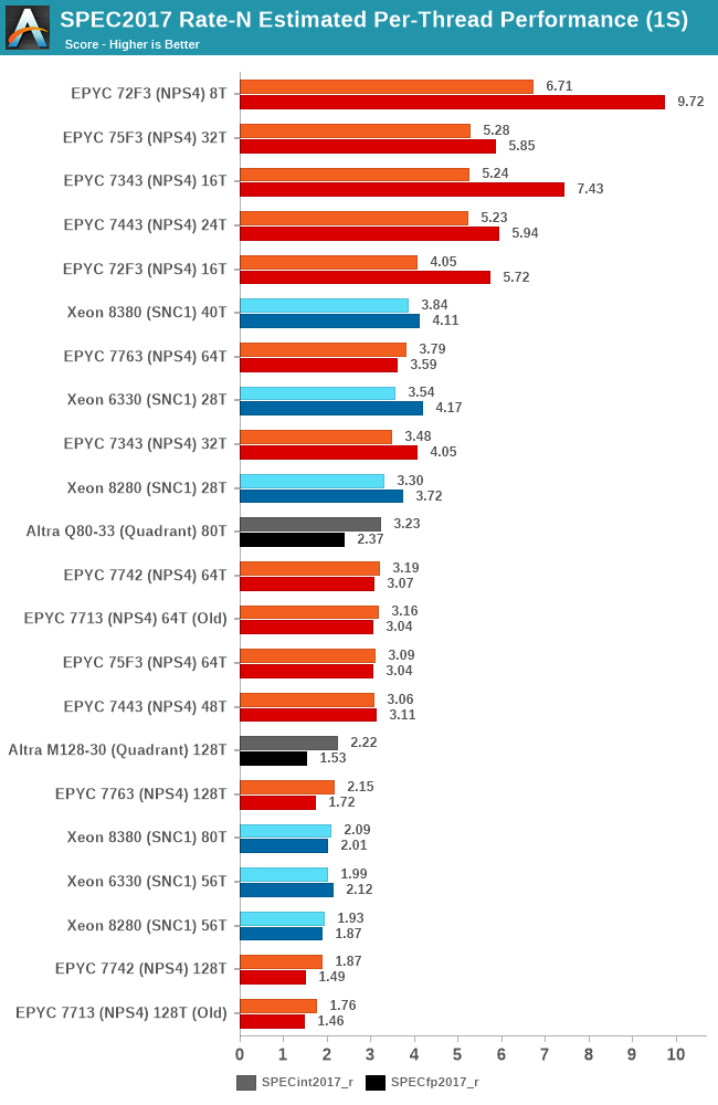
As expected, taking view of the aggregate socket performance figures here, the M128-80 doesn’t fare well here in the metric, as it takes the much controversial “flock of chickens” approach to core performance. It’s also dragged down by the score regressions in the memory bound workload in SPEC.
In terms of total throughput vs per-thread performance, the M128-30 barely differs to the EPYC 7763 with SMT and half the physical cores.
Again, I have to reiterate that these figures are all very much not in favour of the workloads that the Altra Max was designed for – cloud and hyperscaler workloads, which don’t tend to have the same harsher memory demands as some of the workloads in the SPEC suite. However, extracting those workloads in a different subset would also be a questionable practise and actually frowned upon.
The Altra Max here really does need to have huge footnotes in the way that it presents itself.
SPECjbb MultiJVM - Java Performance
Moving on from SPECCPU, we shift over to SPECjbb2015. SPECjbb is a from ground-up developed benchmark that aims to cover both Java performance and server-like workloads, from the SPEC website:
“The SPECjbb2015 benchmark is based on the usage model of a worldwide supermarket company with an IT infrastructure that handles a mix of point-of-sale requests, online purchases, and data-mining operations. It exercises Java 7 and higher features, using the latest data formats (XML), communication using compression, and secure messaging.
Performance metrics are provided for both pure throughput and critical throughput under service-level agreements (SLAs), with response times ranging from 10 to 100 milliseconds.”
The important thing to note here is that the workload is of a transactional nature that mostly works on the data-plane, between different Java virtual machines, and thus threads.
We’re using the MultiJVM test method where as all the benchmark components, meaning controller, server and client virtual machines are running on the same physical machine.
The JVM runtime we’re using is OpenJDK 15 on both x86 and Arm platforms, although not exactly the same sub-version, but closest we could get:
EPYC & Xeon systems:
openjdk 15 2020-09-15

OpenJDK Runtime Environment (build 15+36-Ubuntu-1)

OpenJDK 64-Bit Server VM (build 15+36-Ubuntu-1, mixed mode, sharing)
Altra system:
openjdk 15.0.1 2020-10-20

OpenJDK Runtime Environment 20.9 (build 15.0.1+9)

OpenJDK 64-Bit Server VM 20.9 (build 15.0.1+9, mixed mode, sharing)
Furthermore, we’re configuring SPECjbb’s runtime settings with the following configurables:
SPEC_OPTS_C="-Dspecjbb.group.count=$GROUP_COUNT -Dspecjbb.txi.pergroup.count=$TI_JVM_COUNT -Dspecjbb.forkjoin.workers=N -Dspecjbb.forkjoin.workers.Tier1=N -Dspecjbb.forkjoin.workers.Tier2=1 -Dspecjbb.forkjoin.workers.Tier3=16"
Where N=160 for 2S Altra test runs, N=128 for 1S Altra Max runs, N=80 for 1S Altra test runs, N=112 for 2S Xeon 8280, N=56 for 1S Xeon 8280, and N=128 for 2S and 1S on the EPYC system. The 75F3 system had the worker count reduced to 64 and 32 for 2S/1S runs, with the 7443, 7343 and 72F3 also having the same thread to core ratiio. The Xeon 8380 was running at N=140 for 2S Xeon 8380 and N=70 for 1S - the benchmark had been erroring out at higher thread counts.
In terms of JVM options, we’re limiting ourselves to bare-bone options to keep things simple and straightforward:
EPYC systems:
JAVA_OPTS_C="-server -Xms2g -Xmx2g -Xmn1536m -XX:+UseParallelGC "

JAVA_OPTS_TI="-server -Xms2g -Xmx2g -Xmn1536m -XX:+UseParallelGC"

JAVA_OPTS_BE="-server -Xms48g -Xmx48g -Xmn42g -XX:+UseParallelGC -XX:+AlwaysPreTouch"
Xeon Cascade Lake systems:
JAVA_OPTS_C="-server -Xms2g -Xmx2g -Xmn1536m -XX:+UseParallelGC"

JAVA_OPTS_TI="-server -Xms2g -Xmx2g -Xmn1536m -XX:+UseParallelGC"

JAVA_OPTS_BE="-server -Xms172g -Xmx172g -Xmn156g -XX:+UseParallelGC -XX:+AlwaysPreTouch"
Xeon Ice Lake (SNC1) & Altra systems:
JAVA_OPTS_C="-server -Xms2g -Xmx2g -Xmn1536m -XX:+UseParallelGC"

JAVA_OPTS_TI="-server -Xms2g -Xmx2g -Xmn1536m -XX:+UseParallelGC"

JAVA_OPTS_BE="-server -Xms192g -Xmx192g -Xmn168g -XX:+UseParallelGC -XX:+AlwaysPreTouch"
Xeon Ice Lake systems (SNC2):
JAVA_OPTS_C="-server -Xms2g -Xmx2g -Xmn1536m -XX:+UseParallelGC"

JAVA_OPTS_TI="-server -Xms2g -Xmx2g -Xmn1536m -XX:+UseParallelGC"

JAVA_OPTS_BE="-server -Xms96g -Xmx96g -Xmn84g -XX:+UseParallelGC -XX:+AlwaysPreTouch"
The reason the Xeon CLX system is running a larger back-end heap is because we’re running a single NUMA node per socket, while for the Altra and EPYC we’re running four NUMA nodes per socket for maximised throughput, meaning for the 2S figures we have 8 backends running for the Altra and EPYC and 2 for the Xeon, and naturally half of those numbers for the 1S benchmarks.
For the Ice Lake system, I ran both SNC1 (one NUMA node) as SNC2 (two nodes), with the corresponding scaling in the back-end memory allocation.
The back-ends and transaction injectors are affinitised to their local NUMA node with numactl –cpunodebind and –membind, while the controller is called with –interleave=all.
The max-jOPS and critical-jOPS result figures are defined as follows:
"The max-jOPS is the last successful injection rate before the first failing injection rate where the reattempt also fails. For example, if during the RT-curve phase the injection rate of 80000 passes, but the next injection rate of 90000 fails on two successive attempts, then the max-jOPS would be 80000."
"The overall critical-jOPS is computed by taking the geomean of the individual critical-jOPS computed at these five SLA points, namely:
• Critical-jOPSoverall = Geo-mean of (critical-jOPS@ 10ms, 25ms, 50ms, 75ms and 100ms response time SLAs)
During the RT curve building phase the Transaction Injector measures the 99th percentile response times at each step level for all the requests (see section 9) that are considered in the metrics computations. It then computes the Critical-jOPS for each of the above five SLA points using the following formula:
(first * nOver + last * nUnder) / (nOver + nUnder) "
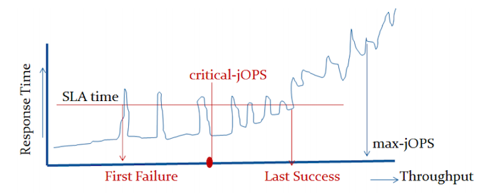
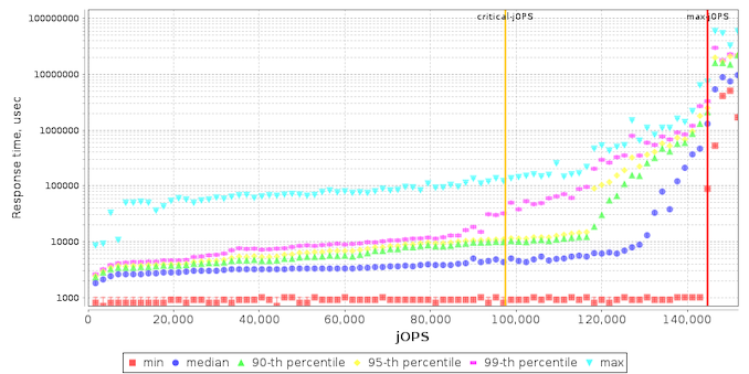
That’s a lot of technicalities to explain an admittedly complex benchmark, but the gist of it is that max-jOPS represents the maximum transaction throughput of a system until further requests fail, and critical-jOPS is an aggregate geomean transaction throughput within several levels of guaranteed response times, essentially different levels of quality of service.
On the SLA graph with the response times across increasing load, we see the Altra Max not differ too much from its predecessor, though it’s simply showcasing improved performance.
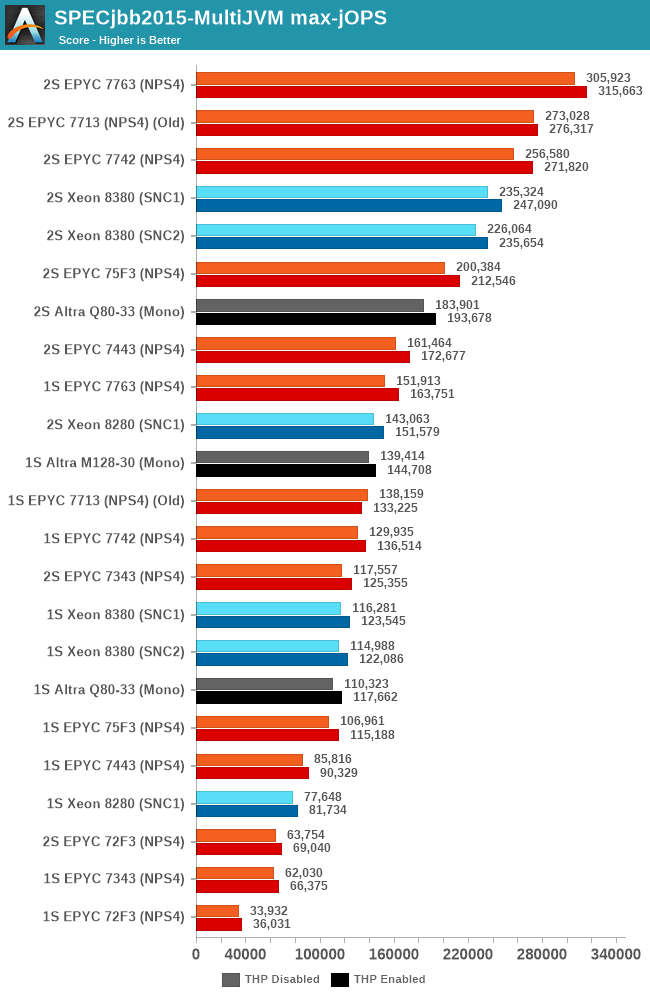
In our initial review of the Q80-33 last year, we had noted that the chip offered lacklustre performance metrics in the SPECjbb benchmark, and though this was somehow attributed to Java performance on AArch64. After spending some more time trying to debug the issue prior to this review, I surprisingly found out that the issue, at least in our configuration, was due to the Altra chip’s operating mode. While we first had tested the chip in quadrant mode, where the chip is partitioned in respective four NUMA nodes, and running four SPECjbb back-ends (one per NUMA node). Running the chip in monolithic mode as an experiment, surprisingly resolved all our performance issues with SPECjbb, with the Q80-33 now running in line where Arm had expected the system to land, which meant increase in the max-jOPS metric and a more massive increase in the critical-jOPS metric as we’ll see in a bit. Unfortunately, trading in one issue with another, we ran into other issues on the 2-socket test scenario where the test ran into issues at large thread counts. The 2S Q80-33 figures here only stresses 130 cores, while I wasn’t able at all to get 2S M128-30 figures at reasonable core counts, so I completely omitted results here.
Focusing on the 1-socket results instead, both the Q80-33 and the new M128-30 now showcase much better performance than what we had seen in the first review of the Altra. The new M128-30 sees a +26% boost in peak throughput performance compared to the Q80-33, however, the chip still lags behind AMD’s flagship EPYC 7763.
The Altra Max here not only is able to increase performance through more cores, but it’s also just outright able to make more usage of its system TDP of 250W. The workload being more data-plane bound, which is also the reason it scales well with SMT, had the effect that the 80-cores on the Q80-33 were running at lower execution resources and lower power, averaging at ~180W, quite below the 250W TDP. The per-core utilisation doesn’t change on the M128-30, but throwing more cores at the matter does help saturate more of the available TDP and result in more performance.
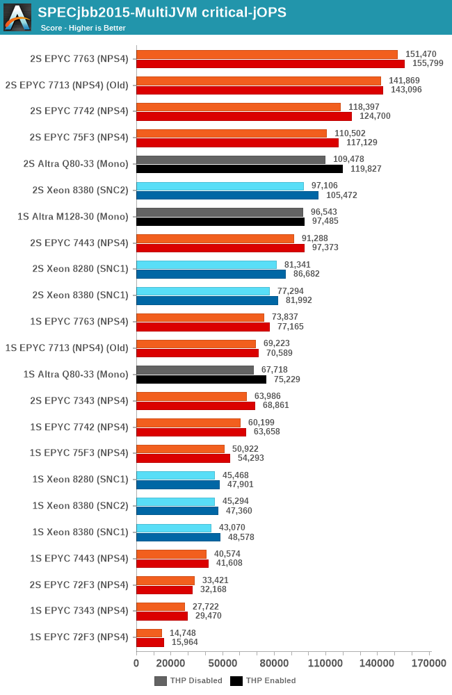
The new critical-jOPS figures for this review are massively improved, with the Q80-33 now posting double that of what we had originally measured. The new M128-30 now further pushes this up, reaching an impressive figure of 96k-jOPS, significantly above the second-best CPU which is the EPYC 7763 at 73k. These new results are much more in line with what we had expected of a single large monolithic CPU design, and showcases the Altra Max in its best possible light and what Ampere tries to focus on – better performance predictability than what the competition can offer with SMT.
We’ll continue to try to figure out what’s happening with the system in the dual-socket scenarios – it’s possible we’re hitting some sort of inherent scaling issue with SPECjbb at these massive thread counts.
Compiling Performance / LLVM
As we’re trying to rebuild our server test suite piece by piece – and there’s still a lot of work go ahead to get a good representative “real world” set of workloads, one more highly desired benchmark amongst readers was a more realistic compilation suite. Chrome and LLVM codebases being the most requested, I landed on LLVM as it’s fairly easy to set up and straightforward.
git clone https://github.com/llvm/llvm-project.gitcd llvm-projectgit checkout release/11.xmkdir ./buildcd ..mkdir llvm-project-tmpfssudo mount -t tmpfs -o size=10G,mode=1777 tmpfs ./llvm-project-tmpfscp -r llvm-project/* llvm-project-tmpfscd ./llvm-project-tmpfs/buildcmake -G Ninja \ -DLLVM_ENABLE_PROJECTS="clang;libcxx;libcxxabi;lldb;compiler-rt;lld" \ -DCMAKE_BUILD_TYPE=Release ../llvmtime cmake --build .We’re using the LLVM 11.0.0 release as the build target version, and we’re compiling Clang, libc++abi, LLDB, Compiler-RT and LLD using GCC 10.2 (self-compiled). To avoid any concerns about I/O we’re building things on a ramdisk – on a 4KB page system 5GB should be sufficient but on the Altra’s 64KB system it used up to 9.5GB, including the source directory. We’re measuring the actual build time and don’t include the configuration phase as usually in the real world that doesn’t happen repeatedly.
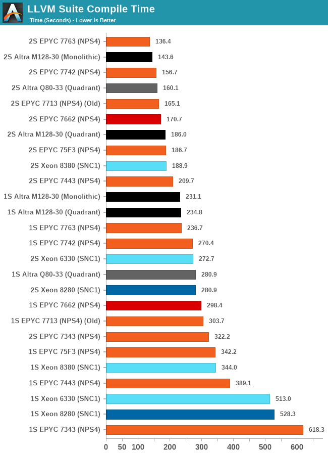
The LLVM compile test results here are quite more special and demand more attention that what meets the eye at first.
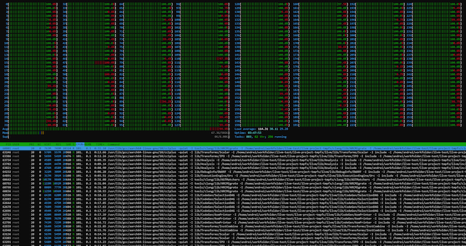
Inherently, the biggest work slice of the test is massively parallel, able to take advantage of all cores in a system, 256 cores in the 2-socket results of the M128-30, however as it’s also a real-world test, the compilation also incurs linking phases where the chip is inherently just under a single-core load and all other cores are just sitting idle.
This behaviour results in some more complex behaviour in the different test scenarios of the M128-30, as the ratio between the parallel/MT and ST phases of the test changes.
In the single-socket results, the chip showcases a +14% performance boost over the Q80-33, while in the 2S results under quadrant mode, this actually transforms into a 16% performance regression. What’s happening here is that while the increased core count of the chip massively helps in improving the actual compilation of objects, the linking phase of the test is significantly slower and takes up a larger percentage of total test time than on the Q80-33, due to the lower CPU frequencies and smaller SLC of the new chip.
Running the M128-30 in monolithic mode actually results in a 24% reduction in compile time, mostly through a large speedup of the linking phase of the compilation as we’re giving that one active core access to the whole 16MB SLC rather than just a 4MB slice.
AMD’s EPYC 7763, even though it has only half the core count, still manages to outperform the M128-30 in the total test time because the linking phase is much sped up thanks to the much superior single-threaded performance of the cores when few threads are active on the SoC. The 34% advantage of the ST SPEC scores here comes more into play than the MT throughput of the chip.
These results are very interesting, and showcase that even in a more real-world scenario like this, the flock-of-chickens approach doesn’t work out as well even in what would consider a massively parallel workload, as some things just cannot be spread out over multiple cores well. It reminds me very much of the eMAG chip, which also suffered in real world code compilations due to the very same reasons.
Conclusion & End Remarks
Our time with the new Altra Max has been interesting, as it’s very much a chip design that quite polarising and pushing some aspects of core scalability to the very extreme.
When Ampere had talked about their plans to put to market a 128-core variant of the Neoverse N1, a 60% increase in cores over their first generation 80-core attempt, we were of course perplexed on how they would achieve this, especially considering the chip is meant to be used on the very same platform with same memory resources, and also on the same fundamental technology – same core microarchitecture, same mesh IP, and same process node.
The Altra Max is a lot more dual-faced than other chips on the market. On one hand, the increase of core count to 128 cores in some cases ends up with massive performance gains that are able to leave the competition in the dust. In some cases, the M128-30 outperforms the EPYC 7763 by 45 to 88% in edge cases, let’s not mention Intel’s solutions.
On the other hand, in some workloads, the 128 cores of the M128 don’t help at all, and actually using them can result in a performance degradation compared to the Q80-33, and also notable slower than the EPYC competition.
I think what we’re seeing here is that Ampere is hyper-optimising themselves into certain workloads. The Altra Max marketing is especially focused around cloud-computing and hyperscaler deployments of the chip. Ampere’s recent announcement earlier this summer, detailing that the company is working on their own custom CPU microarchitecture with specific plans to target such workloads, and abandon the general use case Neoverse Arm CPUs, with Ampere’s description of “general use case” here being mentioned in a negative context, is telling that this is all a deliberate strategy.
What differs a cloud CPU from a regular CPU? I’ll be frank here in mentioning that I don’t have sufficient background on the matter other than to say that memory does not seem to be a focus-point of such workloads. We’re still working on expanding our test suite with more real-world distributed systems workloads to cover such scenarios. By Ampere’s wording of their announcement this summer, and by the very apparent direction of the new Mystique design performance characteristics, it seems we’ll see even greater such extremes in the future.
On the competitive landscape, Ampere is carving out its niche for the moment, but what happens once AMD or Intel increase their core counts as well? A 50% increase in core counts for next-gen Genoa should be sufficient for AMD to catch up with the M128 in raw throughput, and technologies such as V-cache should make sure the HPC segment is fully covered as well, a segment Ampere appears to have no interest in. Intel now has an extremely impressive smaller core in the form of Gracemont, and they could easily make a large-core count server chip to attack the very segment Ampere is focusing on.
Only time will tell if Ampere’s gamble on hyper-focusing on certain workloads and market segments pays out. For now, the new Altra Max is an interesting and very competent chip, but it’s certainly not for everyone.
Related Reading:
-
The Ampere Altra Review: 2x 80 Cores Arm Server Performance Monster
-
AMD EPYC Milan Review Part 2: Testing 8 to 64 Cores in a Production Platform
-
AMD 3rd Gen EPYC Milan Review: A Peak vs Per Core Performance Balance
-
Intel 3rd Gen Xeon Scalable (Ice Lake SP) Review: Generationally Big, Competitively Small

